Báo cáo cuối kỳ môn Computer Architecture and Organization Lab nội dung bằng tiếng Anh | Đại học Sư phạm Kỹ thuật Thành phố Hồ Chí Minh
Báo cáo cuối kỳ môn Computer Architecture and Organization Lab nội dung bằng tiếng Anh của Đại học Sư phạm Kỹ thuật Thành phố Hồ Chí Minh với những kiến thức và thông tin bổ ích giúp sinh viên tham khảo, ôn luyện và phục vụ nhu cầu học tập của mình cụ thể là có định hướng ôn tập, nắm vững kiến thức môn học và làm bài tốt trong những bài kiểm tra, bài tiểu luận, bài tập kết thúc học phần, từ đó học tập tốt và có kết quả cao cũng như có thể vận dụng tốt những kiến thức mình đã học vào thực tiễn cuộc sống. Mời bạn đọc đón xem!
Môn: Computer Architecture and Organization Lab (COOL325364E) 10 tài liệu
Trường: Trường Đại học Sư phạm Kỹ thuật Thành phố Hồ Chí Minh 4.4 K tài liệu
Tác giả:


Preview text:
lOMoARcPSD| 36443508
HCMC UNIVERSITY OF TECHNOLOGY AND EDUCATION
FACULTY FOR HIGH QUALITY TRAINING SUBJECT
Computer Architecture and Organization Lab FINALREPORT lOMoARcPSD| 36443508 TABLE OF CONTENTS
TABLE OF CONTENTS ................................................................................................. 1 TABLE OF FIGURES
..................................................................................................... 4
PART A: 8086 MPU ........................................................................................................ 6
WEEK 1 and WEEK 2:..............................................................................................7 I. Objective
...........................................................................................................7 II. Requirements
...................................................................................................7 III. Design and Implementation
...........................................................................7IV. Results (code &
schematic) ........................................................................... 7 V. Discuss
.............................................................................................................9 WEEK 3:
...................................................................................................................10 I.
Objective .........................................................................................................10 II. Requirements
.................................................................................................10 III. Design and Implementation
.........................................................................10IV. Results (code &
schematic) ......................................................................... 10 V. Discuss
...........................................................................................................14 WEEK 4:
...................................................................................................................15 I.
Objective .........................................................................................................15 II. Requirements
.................................................................................................15 lOMoARcPSD| 36443508 III. Design and Implementation
.........................................................................15IV. Results (code &
schematic) ......................................................................... 15 V. Discuss
...........................................................................................................18 WEEK 5:
...................................................................................................................19 I.
Objective .........................................................................................................19 II. Requirements
.................................................................................................19 III. Design and Implementation
.........................................................................19IV. Results (code &
schematic) ......................................................................... 19 V. Discuss
...........................................................................................................22 WEEK 6:
...................................................................................................................23 I. Objective
.........................................................................................................23 II. Requirements
.................................................................................................23 III. Design and Implementation
.........................................................................23IV. Results (code &
schematic) ......................................................................... 23 V. Discuss
...........................................................................................................26
WEEK 7: ...................................................................................................................27
I. Objective .........................................................................................................27
II. Requirements .................................................................................................27 III. Design and Implementation
.........................................................................27IV. Results (code &
schematic) ......................................................................... 27 V. Discuss
...........................................................................................................29 lOMoARcPSD| 36443508
PART B: 8051 MCU ...................................................................................................... 30
WEEK 8: ...................................................................................................................31
I. Objective .........................................................................................................31
II. Requirements .................................................................................................31 III. Design and Implementation
.........................................................................31IV. Results (code &
schematic) ......................................................................... 31 V. Discuss
...........................................................................................................34
WEEK 9: ...................................................................................................................35
I. Objective .........................................................................................................35
II. Requirements .................................................................................................35 III. Design and Implementation
.........................................................................35IV. Results (code &
schematic) ......................................................................... 35 V. Discuss
...........................................................................................................37
WEEK 10: ................................................................................................................ 38
I. Objective .........................................................................................................38
II. Requirements .................................................................................................38 III. Design and Implementation
.........................................................................38IV. Results (code &
schematic) ......................................................................... 38 V. Discuss
...........................................................................................................40
PART C: HIGH-LEVEL PROGRAMMING ON AT89C51 ........................................41
WEEK 11: ................................................................................................................ 42 I.
Objective .........................................................................................................42
II. Requirements .................................................................................................42 lOMoARcPSD| 36443508 III. Design and Implementation
.........................................................................42IV. Results (code &
schematic) ......................................................................... 42 V. Discuss
...........................................................................................................52
WEEK 12: ................................................................................................................ 54
I. Objective .........................................................................................................54
II. Requirements .................................................................................................54 III. Design and Implementation
.........................................................................54IV. Results (code &
schematic) ......................................................................... 54 V. Discuss
...........................................................................................................61
WEEK 13: ................................................................................................................ 62
I. Objective .........................................................................................................62
II. Requirements .................................................................................................62 III. Design and Implementation
.........................................................................62IV. Results (code &
schematic) ......................................................................... 63 V. Discuss
...........................................................................................................66
WEEK 14: ................................................................................................................ 67
I. Objective .........................................................................................................67
II. Requirements .................................................................................................67 III. Design and Implementation
.........................................................................67IV. Results (code &
schematic) ......................................................................... 68
V. Discuss ...........................................................................................................70
REFERENCES ............................................................................................................... 71 TABLE OF FIGURES lOMoARcPSD| 36443508
Figure: Addition and Subtraction 2 numbers ...................................................................8 Figure: Covert 2 numbers
.................................................................................................9 Figure: Storage addition
of 8-bits register ..................................................................... 12
Figure: Survey instructions such as JMP,JLE and label ................................................13
Figure: Decrease/increase variable value .......................................................................14
Figure: Add and subtract 2 numbers have 2-digits. .......................................................17
Figure: Enter 5 digit numbers from keyboard ................................................................18
Figure: Calculate and storage a 5 digit numbers into a 16-bit register ..........................21
Figure: Enter n bit from keyboard and print exponential 2 ........................................... 22
Figure: Survey Shift 8-bit registers ................................................................................ 24
Figure: Survey Shift 8-bit registers ................................................................................ 26
Figure: Change binary to decimal and print on the screen ............................................ 28
Figure: Change decimal to binary and print on the screen ............................................ 29
Figure: Addition 2 number in 7-segment LED display ................................................. 32
Figure: P2.7 equals 1, Add 2 numbers. .......................................................................... 34
Figure: P2.7 equals 0, Subtract 2 numbers.....................................................................34
Figure : Calculating frequency and duty cycle in the first problem. .............................35
Figure : Frequency and duty cycle of second problem. .................................................36
Figure: Display 7-segment LED by 2Hz ........................................................................39
Figure: Alternating blinking LED ..................................................................................43
Figure : Single LED interface with latch circuit ............................................................45 Figure: Design 7-segment LED
......................................................................................47
Figure: Display 7-segment LED by IC 74LS247 Decoder ............................................48
Figure: Display 7-segments LED by scan method ........................................................ 50
Figure: Scanning 7-segment LED by IC 74245 .............................................................52 Figure: AT89C51 and Button
.........................................................................................55 lOMoARcPSD| 36443508 Figure: AT89C51 and Switch
.........................................................................................56
Figure: Using interrupts to check state when single LED is changed ...........................57
Figure: Using external interrupt to increase the value of LED ......................................59
Figure: Creating precise delay using Timer/Interrupt ....................................................60
Figure: Analog Channel Selection ................................................................................. 62 Figure: Time diagram
..................................................................................................... 62 Figure: Analog to
digital converter ADC ...................................................................... 63
Figure: 8 the sensor temperature LM35 to measure temperature ..................................65
Figure: Virtual Serial Port Driver Software...................................................................67 Figure: H-Term.
..............................................................................................................68 Figure: UART
application ..............................................................................................69 lOMoARcPSD| 36443508 PART A: 8086 MPU
The general purpose of this section is to help learners review some of the issues of
computer architecture from using the design of a computer. In addition, the supported
instruction set architectures for this family of microcontrollers are briefly outlined.
Help learners manipulate the commands supported in the script.
Examine assembly language and the meaning of the process of compiling source code into machine code.
From the basic examples, learners can understand in-depth the usage of each
instruction code, the structure and influence of the registers, as well as the control programming methods such as:
- Move and exchange data, sort, exchange and find elements in arrays.
- Arithmetic processing such as addition, subtraction, multiplication, division Logical processing. - HEX and BCD counters.
- Convert BCD, DEC, HEX digital system. lOMoARcPSD| 36443508 WEEK 1 and WEEK 2: I. Objective
Learn about Assembly language. Understand basic registers.
Understand and use MOV, INT, ADD and SUB instructions. II. Requirements
Can use MOV and INT instructions. Study the ADD and SUB instructions and solve the problem.
Enter two 1-digit numbers from the keyboard in which the first number is larger than
the second one. Calculate the addition and subtraction of them. Algorithm:
- ADD: operand1 = operand1 + operand2.
- SUB: operand1 = operand1 - operand2.
III. Design and Implementation
We use 2 instructions as ADD and SUB to solve the requirement.
After the calculation of results from problem 1, we will change these results into numbers.
IV. Results (code & schematic)
Problem 1: Addition and Subtraction 2 numbers Code: ORG 100H MOV AH,1 INT 21H MOV BH, AL INT 21H MOV BL, AL SUB BX, 3030H ;----ADD MOV CX, BX ADD BH, BL ADD BH, 30H MOV AH, 2 MOV DL, BH INT 21H ;SUB CX, 3030H lOMoARcPSD| 36443508 ;----SUBT SUB CH, CL ADD CH, 30H MOV DL, CH INT 21H RET Solution:
Figure: Addition and Subtraction 2 numbers
Problem 2: Covert 2 numbers Code: ORG 100H MOV AH,1 INT 21H ;AL=37H 00110111B MOV BH,AL ;MOV AH,1 ;DEC. CPI INC. PERF INT 21H ;AL=32H MOV BL,AL ;BX=|A|B| = 3732H ;'7'->7 ; '2'->2
SUB BX, 3030H ;BX=|A|B| = 0702H ADD BH, BL ;BH=09H -> '9' ADD BH, 30H MOV AH, 2 MOV DL, BH INT 21H RET Solution: lOMoARcPSD| 36443508
Figure: Covert 2 numbers V. Discuss
Understanding Assembly programming language.
Understand and use basic registers.
After the problem, we can fluently use the MOV, INT, SUB, ADD instructions.
Moreover, we can fluently use the SUB and ADD instructions and convert numbers to
characters and characters to numbers. WEEK 3: I. Objective
Help learners continue to solve problems using ADD and SUB instruction.
Know is to store the execution result in an 8-bit register. Know how to use labels. II. Requirements
Solve the problem of "Input 2 digits and store in 8-bit register".
III. Design and Implementation
We will use last week's design to solve the question of "Input 2 digits and store in 8-bit register".
Store in 8-bit register using tenth division. lOMoARcPSD| 36443508
In this problem, we will examine the branch instruction and label structure to solve
the problem of storing in 8-bit registers.
IV. Results (code & schematic)
Problem 1: Storage addition of 8-bits register Code: ORG 100H ; NHAP SO 1 MOV AH,1 INT 21H MOV CH,AL INT 21H MOV CL,AL ;CONVERT
;--------------------------------- ; NHAP SO 2 INT 21H MOV DH,AL INT 21H MOV DL,AL
;--------------------------------- ;CONVERT SUB CX,3030H SUB DX,3030H
;--------------------------------MOV AL, 10 MUL CH ADD AL, CL ; GAN GIA TRI TAM THOI MOV BH,AL ; BH= SO THU 1
;--------------------------------MOV AL, 10 MUL DH ADD AL, DL ; GAN GIA TRI TAM THOI MOV BL,AL ; BL = SO THU 2
;--------------------------------MOV CX,BX ;PHEP TINH ADD/SUB ADD BH,BL ; CONG BH=BH+BL ;ADD BL,BH ; CONG BL=BH+BL ;MOV AL,BH lOMoARcPSD| 36443508
;--------------------------------SUB CH,CL ; CH=CH-CL ;MOV BL,CH ; GAN BL = CH
;--------------------------------; PHEP CONG MOV AL,BH MOV DL,10 DIV DL MOV BL,AH MOV AH,0 DIV DL ;-------------------------MOV CL,AH MOV AH,2 MOV DL,AL ADD DL,30H INT 21H MOV DL,CL ADD DL,30H INT 21H MOV DL,BL ADD DL,30H INT 21H ; PHEP TRU MOV AX,0H MOV AL,CH MOV DL,10 DIV DL MOV BL,AH MOV AH,0 DIV DL ;-----------------------MOV CL,AH MOV AH,2 MOV DL,AL ADD DL,30H INT 21H MOV DL,CL ADD DL,30H INT 21H MOV DL,BL ADD DL,30H INT 21H RET lOMoARcPSD| 36443508 Solution:
Figure: Storage addition of 8-bits register
Problem 2: Survey instructions such as JMP,JLE and label. Code: ORG 100H MOV AH,1 INT 21H MOV BH,31H CMP BH,AL JLE STAGE1 JMP EXIT STAGE1: MOV AH,2 MOV DL,AL INT 21H INC BH CMP BH,AL JLE STAGE1 JMP EXIT EXIT: RET Solution: lOMoARcPSD| 36443508
Figure: Survey instructions such as JMP,JLE and label
Problem 3: Applying branching structure to decrease/increase variable value Code: ORG 100H MOV AH,1 INT 21H CMP AL,35H JG DECCASE JLE INCCASE DECCASE: CMP AL,30H JE EXIT DEC AL MOV AH,2 MOV DL,AL INT 21H JGE DECCASE INCCASE: CMP AL,39H JE EXIT INC AL MOV AH,2 MOV DL,AL INT 21H JGE INCCASE EXIT: RET lOMoARcPSD| 36443508 Solution:
Figure: Decrease/increase variable value V. Discuss
We know how to store data in 8-bit registers and examine the principle of branching and label structures.
Understand and use labels well.
Sorting algorithm is more optimal. WEEK 4: I. Objective
Survey MUL and DIV instructions. II. Requirements
Study and can use MUL and DIV instructions to solve the problem. Algorithm: MUL:
- When operand is a byte: AX = AL * operand.
- When operand is a word: (DX AX) = AX * operand. DIV:
- When operand is a byte: AL = AX / operand. AH = remainder (modulus).
- When operand is a word: AX = (DX AX) / operand DX = remainder (modules).
III. Design and Implementation
Survey the MUL and DIV instructions.
Applying multiple and division solve the problems such as storing 0 to 4 digit
numbers in the 16-bit register and entering 5 digit numbers from Keyboard. lOMoARcPSD| 36443508
IV. Results (code & schematic)
Problem 1: Enter 2 numbers have 2 digits. Calculate the addition and subtraction,
print the result to the screen. Code: ORG 100H ;1ST NUMBER MOV AH,1 INT 21H SUB AL,30H MOV DH,10 MUL DH MOV BL,AL MOV AH,1 INT 21H SUB AL,30H ADD BL,AL ;2ND NUMBER MOV AH,1 INT 21H SUB AL,30H MOV DH,10 MUL DH MOV BH,AL MOV AH,1 INT 21H SUB AL,30H ADD BH,AL ;TONG MOV AX,BX ADD AL,AH MOV AH,0 DIV DH MOV CL, AH MOV AH,0 DIV DH MOV DX,AX ;IN RA MAN HINH TONG MOV AH,2 ADD DL,30H INT 21H MOV DL,DH ADD DL,30H lOMoARcPSD| 36443508 INT 21H MOV DL,CL ADD DL,30H INT 21H ;HIEU MOV AX,BX SUB AL,AH MOV DH,10 MOV AH,0 DIV DH MOV BX,AX ;IN RA MAN HINH HIEU MOV AH,2 MOV DL,BL ADD DL,30H INT 21H MOV DL,BH ADD DL,30H INT 21H RET Solution:
Figure: Add and subtract 2 numbers have 2-digits.
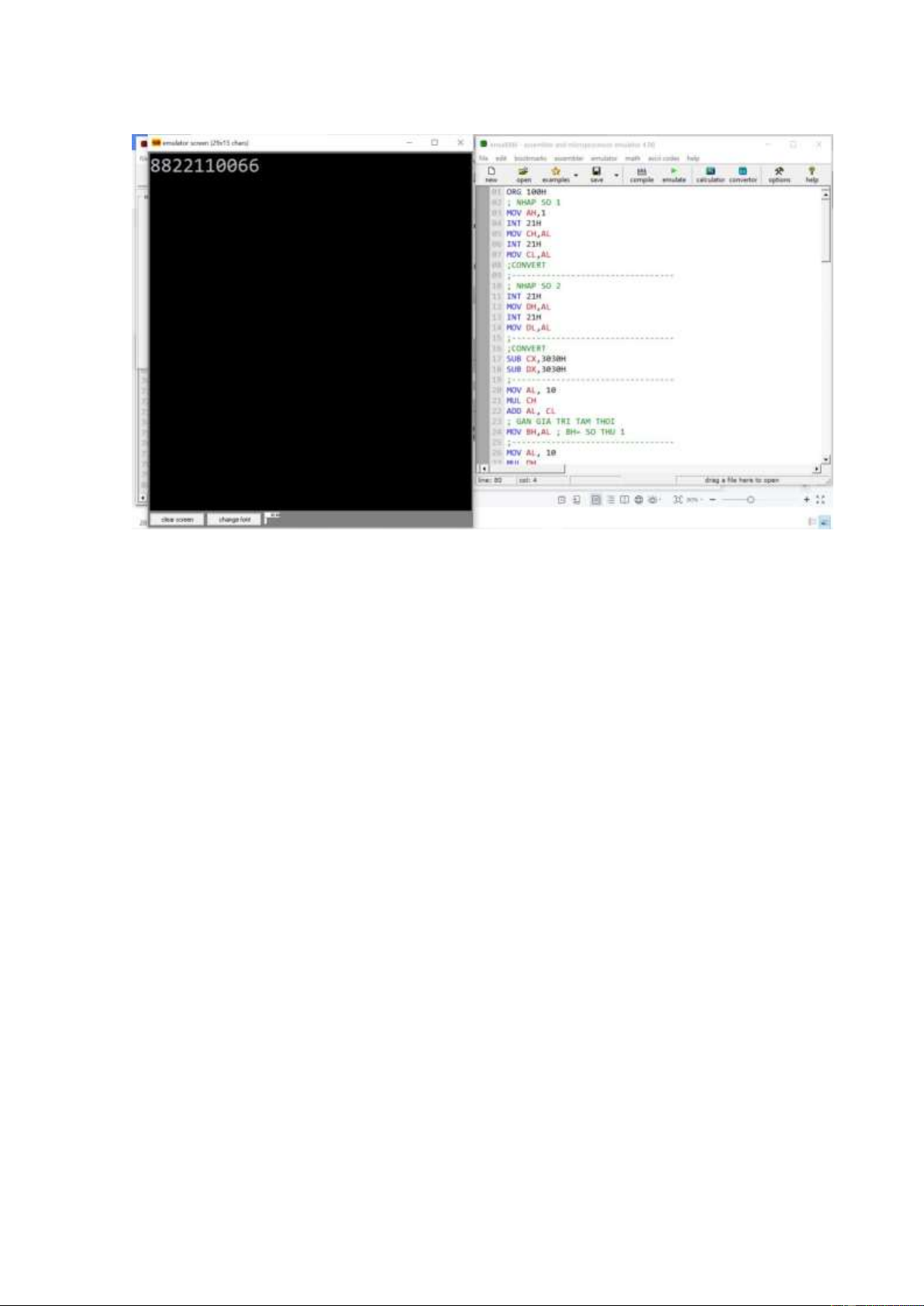
Problem 2: Enter 5 digit numbers from keyboard Code: MOV CX, 0AH INP: MOV AH, 1 INT 21h lOMoARcPSD| 36443508 SUB AL, 30h MOV BH, AL CMP BH, 5h JG Error CMP BH, 1H JL Error MOV DL, 'T' MOV AH, 2 INT 21H MOV DX, 0 COMP: CMP BH, 1 JL EXIT MOV AX, DX MUL CX MOV DX, AX MOV AH, 1 INT 21h SUB AL, 30h MOV AH, 0 ADD DX, AX DEC BH JMP COMP Error: MOV DL, 'F' MOV AH, 2 INT 21H JMP INP EXIT: MOV CX, DX MOV DL, 'D' MOV AH, 2 INT 21H Solution: lOMoARcPSD| 36443508
Figure: Enter 5 digit numbers from keyboard V. Discuss
We can understand how to use multiples and divides in Assembly to solve
questions. Furthermore, learners can design a basic math problem using a combination of instructions. WEEK 5: I. Objective
Introduction to POP and PUSH instructions.
Transfer memory to the Stack using the POP and PUSH instructions. Survey OR, XOR và AND.
Introduction to ROL and SHL instructions. II. Requirements
Solve problems like “Calculating 2n with n:bits”, “Calculating addition or
subtraction and storing in 16 bit registers”.
Complete investigation of instructions such as OR, XOR, AND gates and apply the
investigated transform in the problem. Algorithm:
- POP: operand = SS: [SP] (top of stack) SP = SP + 2
- PUSH: SP = SP - 2 SS: [SP] (top of stack) = operand lOMoARcPSD| 36443508
III. Design and Implementation
The problem: “Calculate and store 5-digit numbers into 16-bit registers”, uses the
POP and PUSH instructions to create loop storage and handle between multiples of
tenths and addition after multiples.
The problem: “Input n bits from the keyboard and print exponential 2”, the main aim
in the design is a combination of LIFO method and ROL and SHL instructions.
IV. Results (code & schematic)
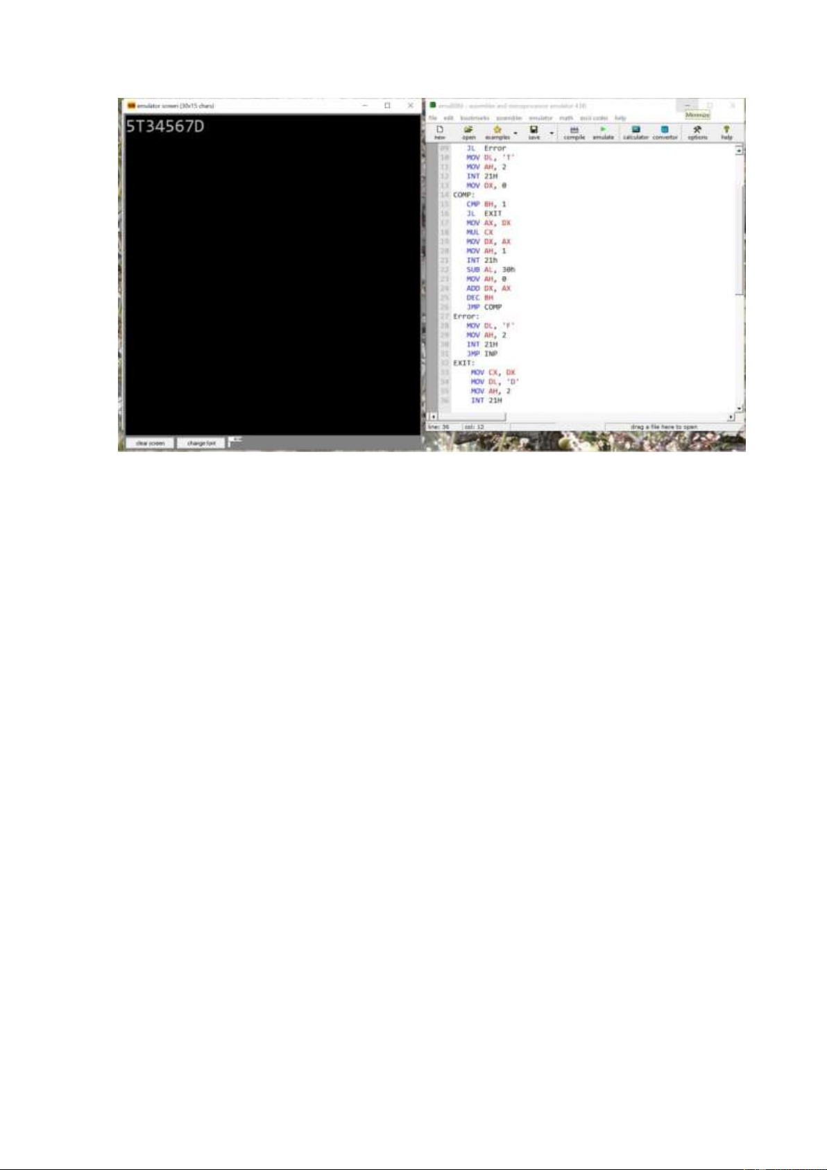
Problem 1: Calculate and storage a 5 digit numbers into a 16-bit register. Code: MOV BL, 2H MAIN: CMP BL, 1H MOV CX, 0H JGE Inp JMP Sum_Sub Store: MOV CX, DX PUSH CX DEC BL MOV AH, 2 MOV DL, 'D' INT 21H JMP MAIN Sum_Sub: POP BX POP CX PUSH BX ADD BX, CX POP DX SUB CX, DX MOV AX,BX ;Start print RET Inp: MOV AX, 00H MOV DX, 00H MOV AH, 1 INT 21h SUB AL, 30h MOV BH, AL lOMoARcPSD| 36443508 JMP Condition Error: MOV AH, 2 MOV DL, 'N' INT 21h JMP Inp Condition: CMP AL, 0H JE Error CMP BH, 4h JG Error Execute: CMP BH, 0H JE Exit MOV AH, 1 INT 21h MOV CL, AL SUB CL, 30h MOV AX, 000Ah MUL DX MOV DX, AX ADD DX, CX DEC BH JMP Execute Exit: CMP BL, 2H JLE Store Solution: lOMoARcPSD| 36443508
Figure: Calculate and storage a 5 digit numbers into a 16-bit register
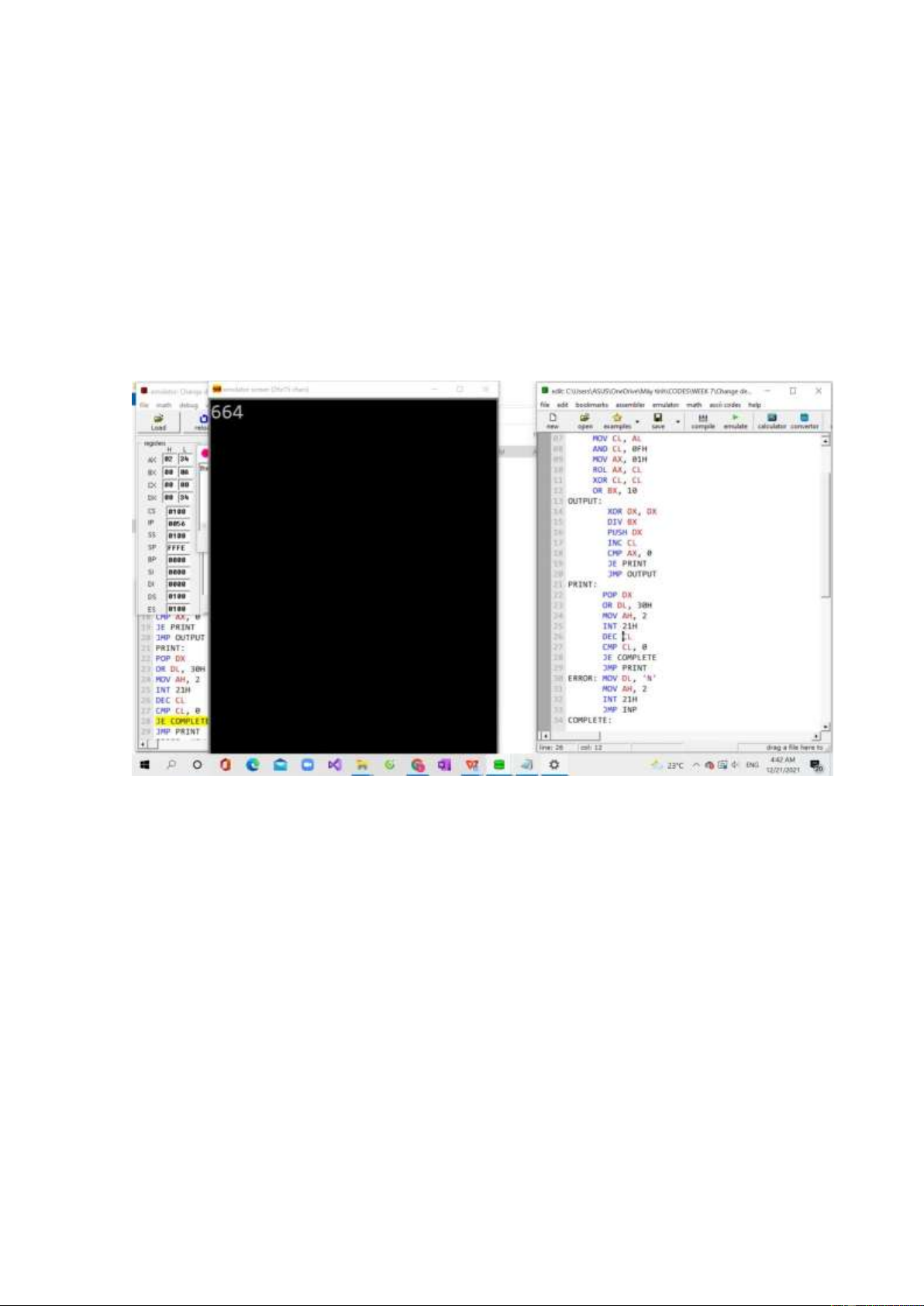
Problem 2: Enter n bit from keyboard and print exponential 2. Code: INP: MOV AH, 1 INT 21H CMP AL, 30H JL ERROR CMP AL, 39H JG ERROR MOV CL, AL AND CL, 0FH MOV AX, 01H ROL AX, CL XOR CL, CL OR BX, 10 OUTPUT: XOR DX, DX DIV BX PUSH DX INC CL CMP AX, 0 JE PRINT JMP OUTPUT PRINT: POP DX OR DL, 30H MOV AH, 2 lOMoARcPSD| 36443508 INT 21H DEC CL CMP CL, 0 JE COMPLETE JMP PRINT ERROR: MOV DL, 'N' MOV AH, 2 INT 21H JMP INP COMPLETE: Solution:
Figure: Enter n bit from keyboard and print exponential 2 V. Discuss Understanding LIFO method.
Understand and use POP and PUSH instructions.
Understand and use ROL and SHL instruction with which we can move any bit in the register.
Manipulate and replace instructions to optimize the algorithm. WEEK 6: I. Objective
Introduction to SHL, SHR, ROL, ROR instructions.
Survey SHL, SHR, ROL, ROR instructions. lOMoARcPSD| 36443508 II. Requirements
Study SHL, SHR, ROL, ROR instructions: For SHL, SHR: Algorithm:
- Shift all bits left, the bit that goes off is set to CF.
- Zero bit is inserted to the right-most position. For ROL, ROR: Algorithm:
- Shift all bits left, the bit that goes off is set to CF, and the same bit is inserted to the right-most position.
III. Design and Implementation
Solve a basic problem: “Survey 8-bit Register Shift and 16-bit Register Shift”.
IV. Results (code & schematic)
Problem 1: Survey Shift 8-bit registers Code: MOV BH,8 MOV CL,0 INPUT: MOV AH,1 INT 21H SUB AX,0030H MOV AH,0H PUSH AX INC CL DEC BH CMP BH,0H JNE INPUT MOV CH,CL MOV CL,0H SUM: POP AX SHL AX,CL INC CL ADD DX,AX MOV BX,DX CMP CH,CL JNE SUM lOMoARcPSD| 36443508 MOV AX,DX ; GAN AX VA CX MOV BX,10 XOR CL,CL CHIA: XOR DX,DX DIV BX PUSH DX INC CL CMP AX,0 JNE CHIA PRINT: POP DX ADD DX,0030H MOV AH,2 INT 21H CMP CL,0 DEC CL JNE PRINT RET Solution:
Figure: Survey Shift 8-bit registers
Problem 2: Survey Shift 16-bit registers Code: INPUT: MOV AH, 1H INT 21H CMP AL, 31H JE SAVE lOMoARcPSD| 36443508 CMP AL, 30H JE SAVE CMP AL, 'b' JE OUTPUT JMP DEL SAVE: AND AL, 0FH XOR AH, AH SHL DX, 1 ADD DX, AX JMP INPUT DEL: XOR DX, DX JMP INPUT OUTPUT: MOV AX, DX ;JMP OUT1 OUT1: MOV BX, 10 XOR DX, DX DIV BX PUSH DX INC CL CMP AX, 0 JE PRINT JMP OUT1 PRINT: POP DX OR DL, 30H MOV AH, 2 INT 21H DEC CL CMP CL, 0 JE EXIT JMP PRINT EXIT: Solution: lOMoARcPSD| 36443508
Figure: Survey Shift 8-bit registers V. Discuss
Understand the knowledge of 8-bit and 16-bit register transfers and rotations.
Learners can use ROL, SHL, ROR and SHR to solve some questions such as
“Designing an exponential circuit”,…
Manipulate and replace instructions to optimize the algorithm. WEEK 7: I. Objective
Review and solve problems using learned instructions. II. Requirements
Understand and use well learned instructions.
Solve the problem by the best method.
III. Design and Implementation
The problem: “Change binary to decimal and print on the screen”.
The problem: “Change decimal to binary and print on the screen”.
IV. Results (code & schematic)
Problem 1: Change binary to decimal and print on the screen Code: OR CL, 16 lOMoARcPSD| 36443508 INP: MOV AH, 1 INT 21H CMP AL, 62H JE CAL CMP AL, 30H JL ERROR CMP AL, 31H JG ERROR AND AL, 0FH XOR AH, AH ROL BX, 1 OR BX, AX DEC CL CMP CL, 0 JE CAL JMP INP ERROR: MOV DL, 'F' MOV AH, 2 INT 21H XOR DX, DX JMP INP CAL: XOR CX, CX MOV AX, BX MOV BX, 0AH OUTPUT: XOR DX, DX DIV BX PUSH DX INC CL CMP AX, 0 JE PRINT JMP OUTPUT PRINT: POP DX OR DL, 30H MOV AH, 2 INT 21H DEC CL CMP CL, 0 JE COMPLETE JMP PRINT COMPLETE: RET Solution: lOMoARcPSD| 36443508
Figure: Change binary to decimal and print on the screen
Problem 2: Change decimal to binary and print on the screen Code: INPUT: MOV AH, 1 INT 21H CMP AL, 'd' JE CONT MOV CL, AL SUB CX, 0030h MOV AX, 000Ah MUL DX MOV DX, AX ADD DX, CX INC BH CMP BH, 4 JNE INPUT CONT: MOV BX,DX CONVERT:ROL BX,1 MOV DL,01H AND DX,BX OR DL,30H MOV AH,2 INT 21H INC CH CMP CH,16 JNE CONVERT EXIT: lOMoARcPSD| 36443508 Solution:
Figure: Change decimal to binary and print on the screen V. Discuss
Understand combinations using instructions and solve basic problems optimally.
Know, understand and apply low-level language well to communicate with computers.
Learners can understand and convert binary and decimal numbers. PART B: 8051 MCU
Introduction to microcontroller communication and basic I/O peripherals such as single switch/LED.
Introduces the basic arithmetic instructions for addition and subtraction, comparison
and branching instructions supported in the microprocessor ALU.
Understand microcontroller communication and basic I/O peripherals like single switch/LED.
The general purpose of this section is to help learners use the instructions supported
in the instruction set of the 8051 family of microcontrollers to build basic peripheral
device control and communication programs. such as single LED, 7 segment LED, matrix key, ... lOMoARcPSD| 36443508 WEEK 8: I. Objective Introducing EDSIM software.
Introduction of 8051 architecture by EDSIM software.
Introduction to the instructions for moving and exchanging data on the 8051 family of microcontrollers.
Introduction to arithmetic operations and calculations.
Write basic code and connect to peripherals. II. Requirements
Understand instructions to move and exchange data in memory.
Understand how to connect any PORT in 8051 to any peripheral.
Design a simple firmware program using assembly language for 8051 family
microcontrollers to perform data transfer and exchange.
III. Design and Implementation
Design circuit, control to connect any PORT with 7-seg LED, single LED… in Assembly language.
IV. Results (code & schematic)
Problem 1: Write a program taking the addition of 2 4-bit binary numbers to
display to any 7 segment-LED. 2 binary numbers are defined by a switch in P2. Code: MOV 40H, #0C0h MOV 41H, #0f9h MOV 42H, #0a4h MOV 43H, #0b0h MOV 44H, #99h MOV 45H, #92h MOV 46H, #82h MOV 47H, #0f8h MOV 48H, #80h MOV 49H, #90h MOV A, P2 ; 01110010 A=2; B=7 MOV 30H, A ANL 30H, #0FH ;NUMBER A ANL A, #0F0H lOMoARcPSD| 36443508 SWAP A ;NUMBER B ADD A, 30H ORL A, #40H MOV R0, A MOV A, @R0 MOV P1, A Schematic:
Figure: Addition 2 number in 7-segment LED display
Problem 2: Enter 2 numbers A, B (3-bit) using P2 in which switch 3 is not used and
switch 7 is used to compare. B ranges from switch 6-4 and A ranges from switch 2- 0. Code: MOV 30H,#0C0H MOV 31H,#0F9H MOV 32H,#0A4H MOV 33H,#0B0H MOV 34H,#99H MOV 35H,#92H MOV 36H,#82H MOV 37H,#0F8H MOV 38H,#80H MOV 39H,#90H ;NUMER OF LED MOV A,P2 ANL A,#70H SWAP A MOV 41H,A ;NUMBER 1 MOV A,P2 lOMoARcPSD| 36443508 ANL A,#07H MOV 42H,A ; NUMER 2 JB P2.7, CONG JNB P2.7, TRU CONG: ; CONG 2 SO MOV A, 41H ADD A, 42H MOV 43H, A JB P2.7, CHIA TRU: ; TRU 2 SO NUM1>NUM2 MOV A, 41H SUBB A, 42H MOV 43H, A JB P2.7,PRINT CHIA: MOV A,43H MOV B,#10 DIV AB MOV 41H,A MOV 42H,B MOV R2,#70 PRINT: ; PRINT SCAN LED MOV A,41H ORL A,#30H MOV R0,A MOV A,@R0 ; CHUC CLR P0.7 MOV P1,A MOV P3,#18H SETB P0.7 MOV A,42H ; DON VI ORL A,#30H MOV R0,A MOV A,@R0 CLR P0.7 MOV P1,A MOV P3,#10H SETB P0.7 DJNZ R2,PRINT Schematic: lOMoARcPSD| 36443508
Figure: P2.7 equals 1, Add 2 numbers.
Figure: P2.7 equals 0, Subtract 2 numbers. V. Discuss
Explain the meaning of instructions and the change in values in the registers in the program.
Understand the arithmetic operations/calculation instructions supported on the processor.
Use the assembly language for 8051 family microcontrollers to perform basic
calculations such as addition/subtraction/multiplication/division. WEEK 9: I. Objective
Understand and write a program that generates cyclic pulses with the highest
possible frequency and calculates frequency and duty cycle. II. Requirements
Calculate the number of machine cycles required to execute the program.
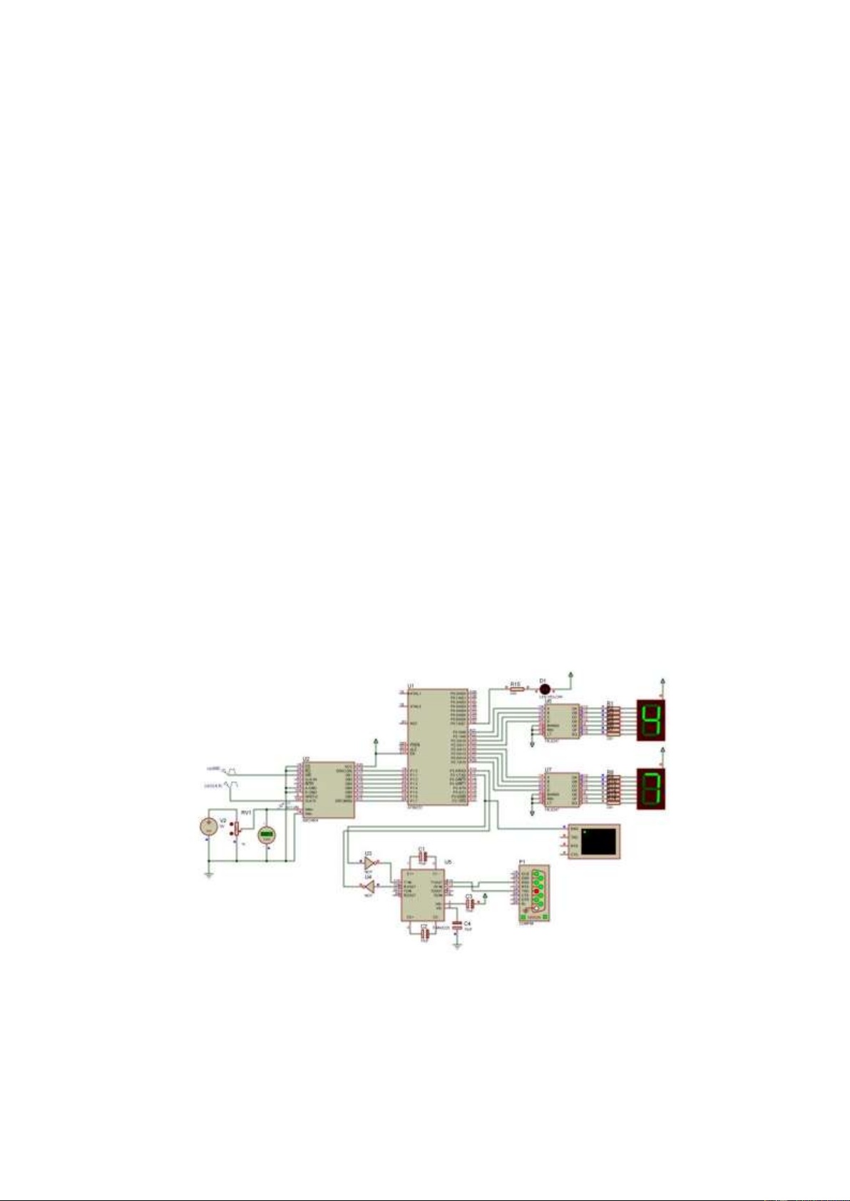
III. Design and Implementation lOMoARcPSD| 36443508
We use IC 8051, buttons, switches and 7-seg LED to simulate a basic circuit. And
we have an Oscilloscope module to measure the frequency of the PORT.
IV. Results (code & schematic)
Problem 1: Survey SET and CLR bit with P1.0 Code: ORG 8100H LOOP: SETB P1.0 CLR P1.0 SJMP LOOP END
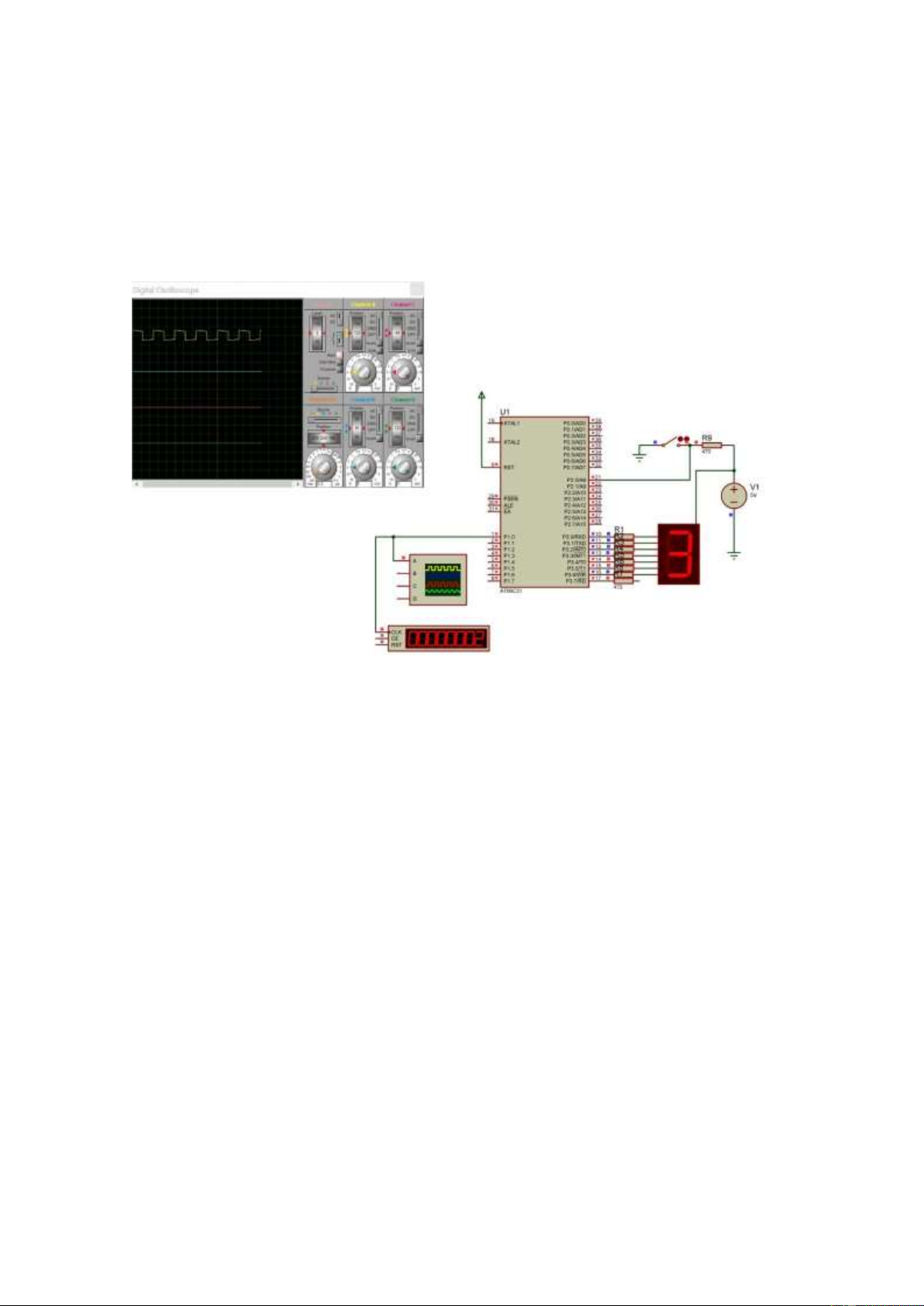
Problem 2: Calculate frequency and duty cycle
Figure : Calculating frequency and duty cycle in the first problem.
Problem 3: Write a program with D=50%, calculate the frequency. Code: LOOP: SETB P1.0 NOP NOP CLR P1.0 SJMP LOOP
Figure : Frequency and duty cycle of second problem. lOMoARcPSD| 36443508
Problem 4: Write a program creating 100KHz with D=50%. Code: Loop: SETB P1.0 NOP NOP NOP NOP CLR P1.0 JMP Loop
Problem 5: Write a program creating 10KHz with D=50%. Code: org 0100h Start: MOV TMOD, #02H MOV TL0, #0D3H SETB TR0 Loop: JNB TF0, Loop CPL P1.0 CLR TF0 MOV TL0, #0D3H JMP Loop END
Problem 6: Write a program creating 1KHz with D=50%. Code: org 0100h Start: MOV TMOD, #01H MOV TH0, #0FEH MOV TL0, #13H SETB TR0 Loop: JNB TF0, Loop CPL P1.0 CLR TF0 MOV TH0, #0FEH MOV TL0, #13H JMP Loop END
Problem 7: Write a program creating 1Hz with D=50%. lOMoARcPSD| 36443508 Code: org 0100h Start: MOV TMOD, #01H MOV TH0, #03CH MOV TL0, #0B8H SETB TR0 MOV R0, #0AH Loop: JNB TF0, Loop CLR TF0 MOV TH0, #03CH MOV TL0, #0B8H DJNZ R0, Loop CPL P1.0 MOV R0, #0AH SJMP Loop END V. Discuss
Understand what principle of the timer is active and the calculation of frequency Timer.
Generate pulses of different frequencies with duty cycle = 50%.
Design and run basic circuits. WEEK 10: I. Objective
Solved the problem was "Display 7-segment LED by 2Hz". II. Requirements
Explain the meaning of instructions and changes in values in registers.
Calculate the number of machine cycles required to execute the program. III.
Design and Implementation
We use IC 8051, buttons, switches and 7-seg LEDs to simulate a basic circuit. And
we have an Oscilloscope module to measure the frequency of the PORT.
The frequency will determine the speed of the 7-seg LED. IV.
Results (code & schematic)Code: org 0000h jmp Start lOMoARcPSD| 36443508 START: MOV 30H, #0C0h MOV 31H, #0F9h MOV 32H, #0A4h MOV 33H, #0B0h MOV 34H, #99h MOV 35H, #92h MOV 36H, #82h MOV 37H, #0F8h MOV 38H, #80h MOV 39H, #90h CLR P1.0 MOV R0,30H GIVE: MOV P3, @R0 JB P2.0, SUB JNB P2.0,PLUS CONS: MOV R1,#5 SET_TIMER: MOV TMOD,#01H MOV TH0, #3CH MOV TL0, #0B0H SETB TR0 LOOP: JNB TF0, LOOP CLR TF0 DJNZ R1, SET_TIMER CPL P1.0 SJMP GIVE PLUS: MOV A,R0 ANL A,#0FH INC A MOV R3,A CJNE R3,#10,SET_A0 MOV R3,#0H MOV A,#0 JMP SET_A0 SUB: MOV A,R0 ANL A,#0FH MOV R3,A JZ SET_A DEC A SJMP OUT lOMoARcPSD| 36443508 SET_A0: SJMP OUT SET_A: MOV A,#9 OUT: ORL A,#30H MOV R0,A SJMP CONS END Schematic:
Figure: Display 7-segment LED by 2Hz V. Discuss
Understand and apply how to communicate between 8051 and peripheral devices
using Assembly language using Timers, 7-seg LED, … Generates a pulse with a frequency of 2Hz.
Design and connect peripheral devices. lOMoARcPSD| 36443508
PART C: HIGH-LEVEL PROGRAMMING ON AT89C51
For the past 10 weeks, we have learned and practiced Assembly language on emu8086 software.
From week 11, we will examine microcontrollers (specifically 8051
microcontrollers) using C programming language.
The general purpose of this section is to apply the high-level programming language
C to program microcontrollers. The examples are intended to help us access the internal
hardware structure of this type of computer. This section will cover more about the
diversification of peripheral devices that can be connected to computers on the 8051
family chip as well as issues illustrating memory expansion communication.
In addition, communication and data exchange between general purpose computers
and computers on the 8051 family are also covered in this section.
From the basic examples provided in this section, we can understand in depth the
usage of each instruction code, the structure and influence of the registers, as well as the
control programming method when executing the instructions tasks from a computer on the 8051 chip.
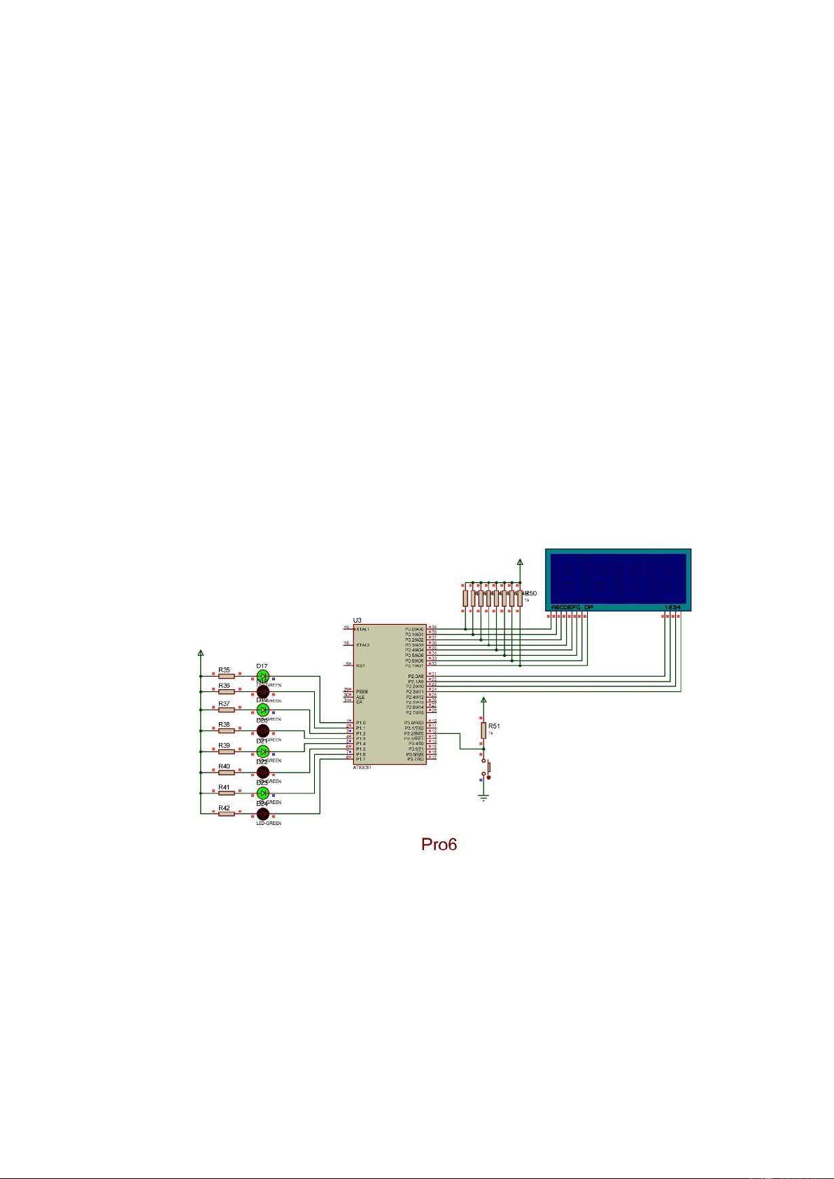
We programmed 8051 microcontroller to communicate with peripheral devices such
as 7-segment LED, LCD, scan LED, Buttons, LM35, ... by Proteus Software and Keli C V5. WEEK 11: I. Objective
Introduction to microcontroller interface and single LED peripheral in different forms.
Introduction to some simple effects that can be done with single LED. II. Requirements
Understand microcontroller interface and single LED peripheral.
Design a simple firmware program using C high level programming language for
8051 family microcontrollers (computer on chip) to interface with single LED.
Know how to analyze and select the value for the LED connection resistor if the supply voltage VDD is 5V. lOMoARcPSD| 36443508
Understand the function of delay function in delay source code.
III. Design and Implementation Single LED
We write a function to set delay time for displaying LED in each case in alternating blinking.
We export or set P0 = 0x55 and delay about 100ms. After that, it changes to next case which at P0 = 0xAA. 7-segment LED
We create an array which contain hexadecimal numbers to export to 7-segment LED by PORT 0 and PORT 2.
Next, we have 2-segment LEDs for unit and decimal numbers in order to need to
create 2 function decoder and display. Decoder usually use to distinguish between unit
and decimal numbers by division of remainder and quotient respectively.
Finally, we base on the 2 functions above and an array to write the displaying 7-
segment LED in the main function. IV. Results (code & schematic) a) Single LED
Problem 1: Design a single LED communication principle diagram by low-level LED active method. Code: #include void delay(int interval) { int i,j; for(i=0;i<255;i++) { for(j=0;j} } void main() { while(1) { P0=0x55; delay(100); P0=0xAA; delay(100); } } lOMoARcPSD| 36443508 Schematic:
Figure: Alternating blinking LED
In this design, use PORT 0 in AT89C51 connection to make LED turn on low state.
Because the AT89C51 receives external power, the single LED must receive a low level
signal from the AT89C51 to activate.
Problem 2: Design a single LED communication principle diagram by high-level LED active method Code: #include #include #define LED0 P1_0 #define LED1 P1_1 #define LED2 P1_2 #define LED3 P1_3 #define LED4 P1_4 #define LED5 P1_5 #define LED6 P1_6 #define LED7 P1_7 #define sang 1 #define tat 0 void delay(unsigned int ms) { unsigned int i,j; for(i=0;ifor(j=0;j<120;j++ ) {} lOMoARcPSD| 36443508
} void display_LED(unsigned char number) { switch(number) { case 1: LED0 = sang;
LED1 = LED2 = LED3 = LED4 = LED5 = LED6 = LED7 =
tat; break; case 2: LED1 = sang;
LED0 = LED2 = LED3 = LED4 = LED5 = LED6 = LED7 =
tat; break; case 3: LED2 = sang;
LED1 = LED0 = LED3 = LED4 = LED5 = LED6 = LED7 =
tat; break; case 4: LED3 = sang;
LED1 = LED2 = LED0 = LED4 = LED5 = LED6 = LED7 =
tat; break; case 5: LED4 = sang;
LED1 = LED2 = LED3 = LED0 = LED5 = LED6 = LED7 =
tat; break; case 6: LED5 = sang;
LED1 = LED2 = LED3 = LED4 = LED0 = LED6 = LED7 =
tat; break; case 7: LED6 = sang;
LED1 = LED2 = LED3 = LED4 = LED5 = LED0 = LED7 =
tat; break; case 8: LED7 = sang;
LED1 = LED2 = LED3 = LED4 = LED5 = LED6 = LED0 = tat; break; } } void main() { unsigned char m; while(1) { for(m=0;m<9;m++) { display_LED(m); delay(500); } } } Schematic: lOMoARcPSD| 36443508
Figure : Single LED interface with latch circuit
We use PORT 0 and PORT 2 to display 7-segment LED and PORT 0 deals with as
unit number and PORT 2 is a tens number.
We create an array containing hexadecimal numbers to output 7-segment LED
according to PORT 0 and PORT 2. Next we have 2 7-segment LEDs for units and tens
to decode and display. Decoders are often used to distinguish between units and decimal
numbers by dividing the remainder and the corresponding quotient. b) 7 segment LED
Problem 1: Direct connection method, connect to common Anode 7-segment LED. Code: #include #define ucharunsignedchar #define uint unsignedint void delay_ms(uint x); void giaima(void); void hienthi(void); uchar donvi,chuc; uint i,j,a; int
dig[]={0xC0,0xF9,0xA4,0xB0,0x99,0x92,0x82,0xF8,0x80,0x90}; void main(void) { while(1) { for(i=0;i<100;i++) { a=i; for(j=0;j<5000;j++) lOMoARcPSD| 36443508 { giaima(); hienthi() ; } } } } void delay_ms(uint x) { uchar k; while(x-- >0) { for(k=0;k<125;k++) {} } } void giaima(void) { chuc=a/10; donvi=a%10; } void hienthi(void) { P0=dig[donvi]; P2=dig[chuc]; } Schematic:
Figure: Design 7-segment LED
We use PORT 0 and PORT 2 to display 7-segment LED and PORT 0 deals with as
unit number and PORT 2 is a tens number. lOMoARcPSD| 36443508
We create an array containing hexadecimal numbers to output 7-segment LED
according to PORT 0 and PORT 2. Next we have 2 7-segment LED for units and tens to
decode and display. Decoders are often used to distinguish between units and decimal
numbers by dividing the remainder and the corresponding quotient. Problem 2:
Connection method using decoder, connect to 7 segment LED common anode. IC
74LS47 and IC 7446 are decoding from BCD code to 7-segment code. Code: #include int dem=0;
void delay(unsigned long time) { unsigned long i; for(i=0;i; {} } void main(void) { P2=0x00; while(dem<10) { P2=dem; dem++; delay(10000) ; } } Schematic: lOMoARcPSD| 36443508
Figure: Display 7-segment LED by IC 74LS247 Decoder
In this case, we use IC 74LS247 decoder, the encoder programming is easier than
direct connection in problem 1, so we just need to create a count function from 0 to 9 in
PORT2 and IC 74LS247 will automatically decode to decimal and displayed by 7- segment LED.
Problem 3: Direct connection method combines scanning for multiple 7-segment
LEDs. Use LED scanning method to display. Code: #include #include #define DELAYTIME 65000 unsigned int temp1; void delay(unsigned int temp) { while(--temp); } void main() { P1=0; //LED is off while(1) { P1=1; P2=0XC0; temp1 = DELAYTIME; delay(temp1); P1 = 2; P2 = 0XF9; temp1 = lOMoARcPSD| 36443508 DELAYTIME; delay (temp1); P1 = 4; P2 = 0XA4; temp1 = DELAYTIME; delay(temp1); P1 = 8; P2 = 0XB0; temp1 = DELAYTIME; delay (temp1); P1 = 1; P2 = 0X99; temp1 = DELAYTIME; delay (temp1); P1 = 2; P2 = 0X92; temp1 = DELAYTIME; delay (temp1); P1 = 4; P2 = 0X82; temp1 = DELAYTIME; delay (temp1); P1 = 8; P2 = 0Xf8; temp1 = DELAYTIME; delay (temp1); P1 = 1; P2 = 0X80; temp1 = DELAYTIME; delay (temp1); P1 = 2; P2 = 0X90; temp1 = DELAYTIME; delay (temp1); P1 = 4; P2 = 0X08; temp1 = DELAYTIME; delay (temp1); P1=8; P2=0X03; temp1 = DELAYTIME; delay (temp1); P1 = 1; P2 = 0X46; temp1 = DELAYTIME; delay (temp1); lOMoARcPSD| 36443508 P1 = 2; P2 = 0X21; temp1 = DELAYTIME; delay (temp1); P1 = 4; P2 = 0X06; temp1 = DELAYTIME; delay (temp1); P1 = 8; P2 = 0X0E; temp1 = DELAYTIME; delay (temp1); temp1 = DELAYTIME; delay (temp1); } } Schematic:
Figure: Display 7-segments LED by scan method
We use PORT 1 and PORT 2. At PORT2, the signal hexadecimal is exported to 7-
segment LED while PORT1 use to turn on or off 7-segment LED which are powered
through CMOS NPN. when we set variable P1.0 = 0, CMOS NPN receives a signal high
level and makes the transistor of the gate is closed to transmit the source to the common
anode of the 7-segment LED. And then, we will display the expected number by giving
signal from PORT 2 to 7-segment LED and use PORT 1 to select the channel to show it. lOMoARcPSD| 36443508
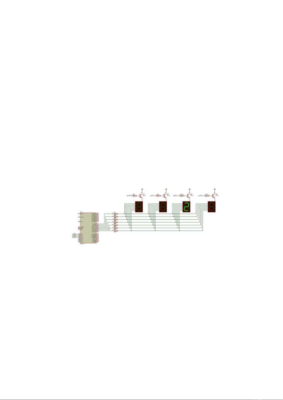
Problem 4: The method combines LED scanning and using IC 74245 Code: #include void delay() { int i; for(i=1;i<200;i++); }
unsignedcharnum[10]={0xC0,0xF9,0xA4,0xB0,0x99,0x92,0x82, 0xF8,0x80,0x90}; void main() { int x,m,n,j,i = 0; unsigned char p0; while(1) { i=0;n=0;m=0;j=0; for(m=0;m<10;m++) for (n=0;n<10;n++) for (i=0;i<10;i++) for (j=0;j<10;j++) for(x=100;x>0;x--) { P0 = num[j]; P1 = 0xfe; delay(); P1 = 0xff; P1 = 0xfd; P0 = num[i]; delay(); P1 = 0xff; P1 = 0xfb; P0 = num[n]; delay(); P1 = 0xff; P1 = 0xf7; P0 = num[m]; delay(); P1 = 0xff; } } } Schematic: lOMoARcPSD| 36443508
Figure: Scanning 7-segment LED by IC 74245
In this case, we combine IC 74LS245 and AT89C51 to scan 7-segment LED in the
circuit. As we can see, IC AT89C51 uses PORT 1.0 - 1.3 to choose to turn on / off each
7-segment LED while PORT 0 transmits the signal to the input of 7-segment LED to display.
We create an array containing hexadecimal numbers to display to 7-segment LED
according to PORT 0 and PORT 2. Next, we use the method in problem 2 and 3 to scan
the 7-segment LED sequentially but in the lesson. In problem 4, we apply IC 74LS245
for low signal operating through NOT GATE. When outputting data from PORT 0 into
7-segment LED, PORT 1.0-1.3 is selected continuously to turn on/off each 7-segment
LED because IC 74LS245 activates low. Finally, we repeat this process continuously to scan the 7-segment LED. V. Discuss
To connect IC AT89C51 with peripherals there are 2 ways: problem 1 shows us how
to display LED directly connected to AT89C51 and problem 2 uses latch circuit to hold
and output signal by IC 74LS245 at high level.
Problems 1 and 2 show us how to directly connect a 7-segment LED to IC AT89C51. lOMoARcPSD| 36443508
Problems 3 and 4 show us how to connect 7 segments by scanning and using IC
74LS245 to buffer the current in the circuit. In the scanning method, we can reduce the
number of ports connected by peripheral devices such as 7-segment LED, single LED,… lOMoARcPSD| 36443508 WEEK 12: I. Objective
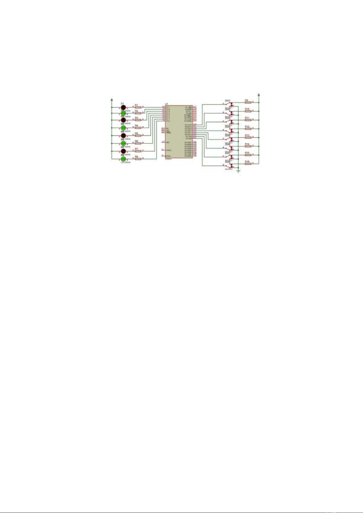
Introduce the method of switching switch with the microcontroller to input the push button input peripheral.
Introduction to matrix keyboard communication method with microcontroller.
Introduction to peripheral communication methods using external interrupts.
Introduces a method to use a timer timer to generate an accurate delay. II. Requirements
Understand the difference between the communication method because it uses the
concept of INTERRUPT Understand the machine cycle (MC) and the combination of
MC with TIMER to create delay.
Design a simple firmware program using the high-level C programming language
for the 8051 family (computer-on-chip) microcontrollers to apply INTERRUPT and TIMER programming.
III. Design and ImplementationConnect peripherals.
7 segment LED status display by push button.
Single LED display by switch button.
Use interrupts to check the state when a single LED is changed.
Use an external interrupt to increase the value of the LED.
Generate precise delay using Timer/Interrupt.
IV. Results (code & schematic)
Problem 1: Push button method. When button B2 (input P1.0) is 0. Code: #include void delay(int interval) { int i,j; for(i=0;i<255;i++) { for(j=0;j} } void main() { while(1) {
//Kiem tra trang thai chan P1_0 (dau voi cong tac) if(P1_0 == 1) lOMoARcPSD| 36443508 { P0=0x55; delay(10); P0=0xAA; delay(10); } } } Schematic:
Figure: AT89C51 and Button
We can see that that button has an important role in changing the state of every LED.
When we turn on / off the button, the 7-segment LED will change immediately according to the preset.
Problem 2: Display single LED by switching button Code: #include void main() { unsigned char temp; P1=0XFF; P2=0XFF; while(1) { temp=P2; P1=temp; while(P2==temp) ; } lOMoARcPSD| 36443508 } Schematic:
Figure: AT89C51 and Switch
We set up 8 switches to change value of single led that based on low and high levels
of the input data of IC AT89C51.
Problem 4: Apply interrupt and display 7-segment LED Case 1:
Using interrupts to check state when single LED is changed. Code: #include void SetupEx0(void); void main(void) { SetupEx0() ; while(1); } void SetupEx0(void) { EA=0; IT0 = 1; EX0=1; EA = 1; } void Ex0Isr(void) interrupt 0 { P1_0 = !P1_0; lOMoARcPSD| 36443508 } Schematic:
Figure: Using interrupts to check state when single LED is changed
We connect PORT 3.2 with button and PORT 3.2 and 3.3 is one of interrupt mode
which to setup to interrupt when it receives a signal data.
Case 2: Using external interrupt to increase the value of LED. Code: #include int count=0; void delay(int interval) { int i,j; for(i=0;i<100;i++) { for(j=0;j} }
void output_7seg(unsigned char value) { unsigned char const
mask[10]={0xC0, 0xF9, 0xA4, 0xB0, 0x99, 0x92, 0x82, 0xF8, 0x80, 0x90}; if(value < 10) { P0=mask[value]; } }
void EXT0_Process() interrupt 0 lOMoARcPSD| 36443508 { EA=0; count++; EA=1; } void display_number(int iNum) { int i; unsigned char pos=0x08; unsigned char temp; for(i=0;i<4;i++) { temp=iNum%10; iNum=iNum/10; P2=pos; output_7seg(temp) ; delay(5); pos=pos>>1; } } void init() {
P3_2=1; //Thiet lap chan P3_2 lam chan vao
IE=0x81; //Cho phep ngat ngoai IT0=1; //Ngat theo suon } void main() { init(); while(1) {display_number(count);} } Schematic: lOMoARcPSD| 36443508
Figure: Using external interrupt to increase the value of LED
We create an array containing the hexadecimal of the 7-segment LED and an
external interrupt function. We configure the external interrupt mode by “void init ( )”
and count the value when INT0 receives signal data by “void EXT0_Processes ( )”.
Next, we need a function to display the 7-segment LED on the screen as “void
display_number (int iNum)”. Finally, when the button is pressed, the 7-segment LED will change state.
Case 3: Creating precise delay using Timer/Interrupt. Code: #include
//tao do tre chinh xac su dung Timer void delay_hardware_50ms() { TMOD=TMOD & 0xF0; //Xoa thiet lap Timer0 TMOD=TMOD | 0x01; ET0=0; //Khong phat sinh ngat TH0=0x3C;
//Thietlapgiatri khoidaula3CB0 TL0=0xB0; //Tuong duong 15536 he 10 TF0=0; //Xoa co tran timer 0 TR0=1; //Khoi dong timer 0 while(TF0==0); //Cho den khi tran TR0=0; //Dung timer 0 } lOMoARcPSD| 36443508
//Chuong trinh tao tre chinh xac 1s void delay_hardware_1s() { int i; for(i=0;i<20;i++) { delay_hardware_50ms(); } } void main() { while(1) { P1=0xAA; delay_hardware_1s(); P1=0x55; delay_hardware_1s(); } } Schematic:
Figure: Creating precise delay using Timer/Interrupt We
use Timer to set delay of LED by any of below steps like:
- First, we have to clear the timer flag 0 and then set it to 1.
- ET0 is used to prevent interrupts from triggering.
- We can set the LED display time according to the timer through setting registers TH0
and TL0. We use the formula T = 1/f to calculate the required delay time. lOMoARcPSD| 36443508
- From the result of time delay, we attach TH0 and TL0 as desired.
- Set TF0 and TR0 to 0 and 1 respectively to clear the overflow flag and enable the 16-bit timer.
- Check TF0 until it is 1 then set TR0 to 0. TR0 is used to stop 16 bit timer.
- Finally, before the 7-segment LED goes to the next state, it must wait for a time delay by a timer. V. Discuss
In this problem, we understand the method of peripheral communication with
interrupts and understand machine cycle and combine it with timer to create delay.
Design a simple program using the language high level C programming for microcontrollers. lOMoARcPSD| 36443508 WEEK 13: I. Objective
Introduction to microcontroller communication method and analog to digital converter (ADC).
Introduce some simple applications with the ADC0809. II. Requirements
Understand the communication method between the microcontroller and the ADC analog-to-digital converter.
Design a simple firmware program using the high-level C programming language
for 8051 family microcontrollers (computers on a chip) to communicate with the ADC.
III. Design and Implementation
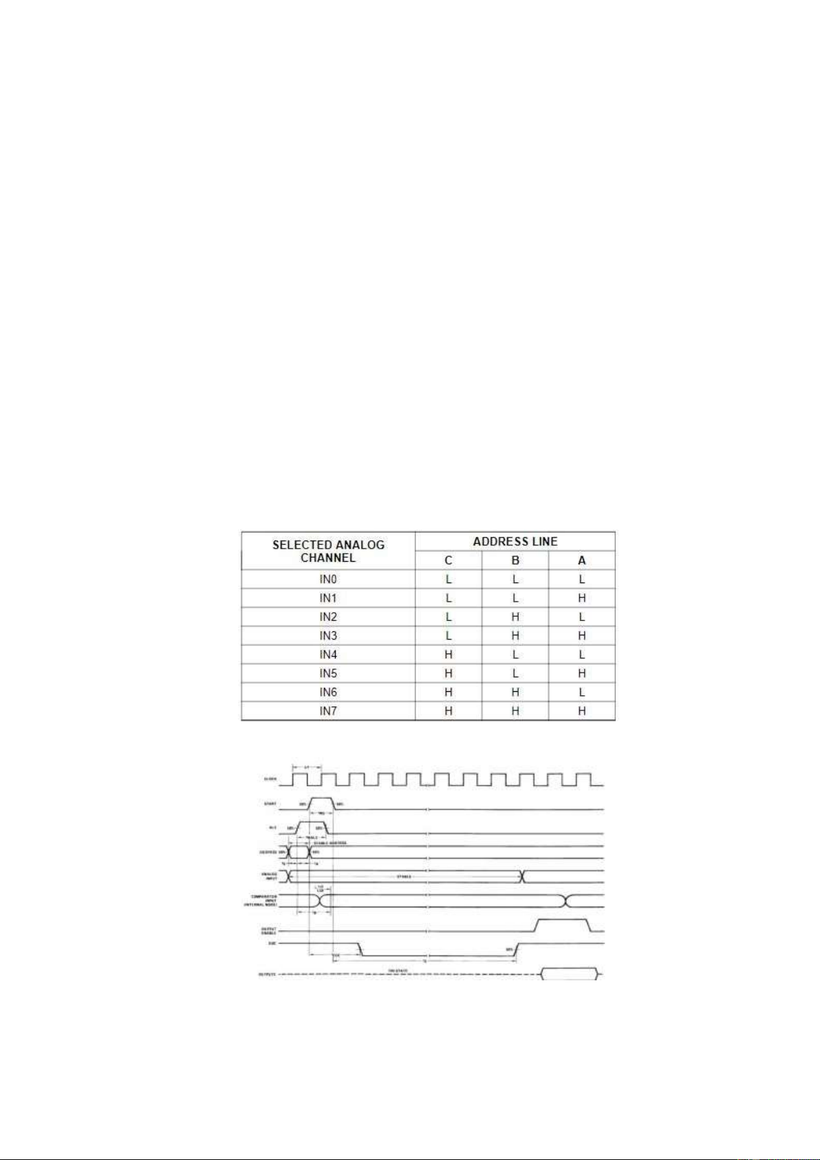
ADC0808 has 8 output data, 3 chip select data to get channel, OE is open enable,
clock pulse, 1 bit START, 1 bit ALE that allow to read input data to output data ,
VREF and 8 input data as temperature, voltage,…
Figure: Analog Channel Selection Figure: Time diagram Formula of converter: lOMoARcPSD| 36443508
- Step size(Dmin) = (+2)(−)(−) - The output code N : N =
(+)−(−) . 2(). +−() Note:
- Total Unadjusted Error: ±½ LSB and ±1 LSB
IV. Results (code & schematic)
Problem 1: Survey operation on analog to digital converter ADC.
Figure : Analog to digital converter ADC Problem
2: Analog to Digital Converters and sensor temperature LM35 Code: #include #define ucharunsignedchar #define uint unsignedint #define port0P0 #define ale P1_0 #define a P1_1 #define b P1_2 #define c P1_3 #define oeP1_4 #define eoc P1_5 #define startP1_6
Int dig[]={0xC0,0xF9,0xA4,0xB0,0x99,0x92,0x82,0xF8,0x80, 0x90}; uchartram,chuc,donvi; uint x; lOMoARcPSD| 36443508 void delay(int x) { int i; for(i=0;i} void tachso(void) { tram=x/100; chuc=(x/10)%10; donvi=x%10; } void giaima(int x) { if (x==1) {c=0;b=0;a=0;} if (x==2) {c=0;b=0;a=1;} if (x==3) {c=0;b=1;a=0;} if (x==4) {c=0;b=1;a=1;} if (x==5) {c=1;b=0;a=0;} if (x==6) {c=1;b=0;a=1;} if (x==7) {c=1;b=1;a=0;} if (x==8) {c=1;b=1;a=1;} } void main() { int i; oe = 1; for(i=0;i<8;i++) { int tam; for(tam=0;tam<30;tam++) { P2=0x01; P0=dig[i+1]; P2_4=0; delay(1000); start=0;ale=0;eoc=1 ; giaima(i+1); delay(100); start=1;ale=1; lOMoARcPSD| 36443508 delay(500); start=0;ale=0; while(eoc==0); delay(100); eoc=1; x=P3; tachso(); P2=0x02; P0=dig[tram]; P2_4=1; delay(500); P2=0x04; P0=dig[chuc]; P2_4=1; delay(500); P2=0x08; P0=dig[donvi]; P2_4=1; delay(500); } } } Schematic:
Figure: 8 the sensor temperature LM35 to measure temperature
We have to set the wires as P1.0, P1.4, P1.5, P1.6 and P1.1 to P1.3 using the same
ports of IC ADC0808. PORT 3 connects to the output data of ADC0808 (OUT1 OUT8)
and the input data of ADC0808 is linked to 8 temperature sensors. lOMoARcPSD| 36443508
From the datasheet, the minimum clock frequency in the ADC0808 is 10kHz and
goes up to 1280kHz. If we set wrong clock input data in ADC0808, it cannot convert the
value of input data to output data. Finally, the circuit will transmit the value of the
temperature to display as a 7-segment LED. V. Discuss
Understand the communication method between the microcontroller and ADC analog.
Design a simple program using the language high level C programming for
microcontrollers family 8051 to communicate with ADC. lOMoARcPSD| 36443508 WEEK 14: I. Objective
Introduction to microcontroller communication methods using UART asynchronous serial data transmission.
Introduction to basic computer communication applications through the UART transmission standard.
Introduction to the function of MAX232 converter in computer communication.
Introduction to the method of building graphical applications (GUI) controlled from the computer. II. Requirements
Understand the communication method between microcontroller and general purpose computer via UART.
Design a simple firmware program using the high-level C programming language
for the 8051 family of microcontrollers (computer on chip) combined with a GUI using
C# to communicate with the computer as well as other microcontrollers.
III. Design and Implementation
In this problem, we use 2 software Virtual Serial Port Driver and H-Term to simulate. lOMoARcPSD| 36443508
Figure: Virtual Serial Port Driver Software
The Virtual Serial Port Driver help the user create Virtual Port such as COM1 and
COM2 communication if they don’t have Physical Port. Figure: H-Term.
H-Term Software is a middleware that helps 2 ports as COM1 and COM2 connect to each other.
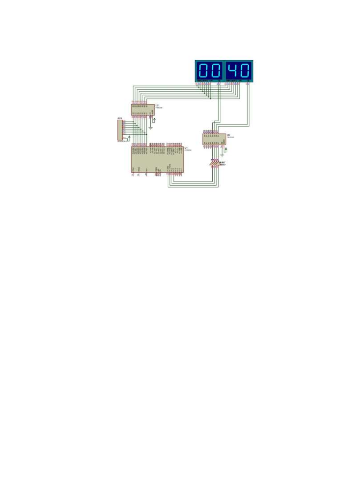
IV. Results (code & schematic) Code: #include
unsigned char chuc, dvi, rdata, nhietdo; void setup() {
TMOD = 0x20;//;enabletimer1,mode2(autoreload) TH1 = -3; //9600Baudrate
SCON = 0x50;//;8bituart,1stop bit,RENenabled,timer1 TR1 = 1; IE = 0x90;
} void serint(void)interrupt 4 using 1 { if(RI) { rdata = SBUF; RI = 0; lOMoARcPSD| 36443508 switch(rdata) { case('0'):{P0_7 = 0; break;} case('1'):{P0_7 = 1; break;} case('a'):{TH1 = -24; break;} case('b'):{TH1 = -12; break;} case('c'):{TH1 = -6; break;} case('d'):{TH1 = -3; break;} } } } void main() { unsigned char trans_data; setup(); while(1) { nhietdo = P1; chuc = (nhietdo/10)<<4; dvi = nhietdo%10; P2 = chuc|dvi; trans_data = P2; SBUF = trans_data; while(TI == 0); TI = 0; } } Schematic:
Figure : UART application
Through the above 2 software, we can transmit and send data back and forth and
output the sent data value displayed on the 7-segment LED. lOMoARcPSD| 36443508
In this problem, we use the temperature read AT89C51 of ADC0804 and display it
in 7-segment LED. The problem will show you how the UART connects the circuit using
a single LED that is activated for identification. V. Discuss
We have interfaced microcontroller using UART, basic computer communication
via UART transmission standard, and understood the function of MAX232 converter in computer communication. lOMoARcPSD| 36443508 REFERENCES
1. Datasheet: AT89C51, ADC0808, Max232, LM35
2. William Stallings, Computer Organization and Architecture 10th Edition,
https://vn1lib.org/book/3710986/989b01
3. Tống Văn On, HỌ VI ĐIỀU KHIỂN 8051,
https://www.kenhebook.info/2016/03/ho-vi-ieu-khien-8051-tong-van-on-pdf.html
4. Phạm Văn Khoa, Thực hành Kiến trúc và Tổ chức Máy Tính.
5. Springer, 8051 Microcontrollers: Fundamental Concepts, Hardware, Software and
Applications in Electronics, https://vn1lib.org/book/3512403/23d0b2.
Tài liệu liên quan:
-

Revise C++: Create Your First OOP Project Guide | Môn Computer Architecture and Organization Lab - Đại học Sư phạm Kỹ thuật Thành phố Hồ Chí Minh
99 50 -

Bài 1 - Lập trình điều khiển đèn giao thông và RTC | Môn Computer Architecture and Organization Lab - Đại học Sư phạm Kỹ thuật Thành phố Hồ Chí Minh
149 75 -

Final Report Môn Computer Architecture and Organization Lab | Đại học Sư phạm Kỹ thuật Thành phố Hồ Chí Minh
126 63 -

Summary of HDL Coding Techniques & Considerations | Môn Computer Architecture and Organization Lab - Đại học Sư phạm Kỹ thuật Thành phố Hồ Chí Minh
135 68 -

Giới thiệu về Dữ liệu, Thông tin và Cơ sở dữ liệu | Môn Computer Architecture and Organization Lab - Đại học Sư phạm Kỹ thuật Thành phố Hồ Chí Minh
100 50