Design of a directional coupler with spurious suppression in extended microstrip | Học viện Kỹ thuận Quân sự
In this article, a tri-band 180-degree directional coupler with spurious suppression is proposed. This coupler is realized using the extended p-shaped Microstrip operating at 3 different frequencies. Design of a directional coupler with spurious suppression in extended microstrip | Học viện Kỹ thuận Quân sự. Tài liệu được sưu tầm gồm 10 trang, giúp bạn tham khảo, ôn tập và đạt kết quả cao!
Môn: Cấu trúc dữ liệu và giải thuật (1222115) 10 tài liệu
Trường: Học viện kỹ thuật quân sự 127 tài liệu
Tác giả:


Preview text:
lOMoAR cPSD| 59256994 1612 | BARIK ET AL .
[5] Lei J, Fu G, Yang L, Fu DM. A modified balanced antipodal
School of Computer and Electrical Engineering, Indian Institute of
Vivaldi antenna with improved radiation characteristics.
Information Technology Design and Manufacturing, Kancheepuram, Chennai 600127, India
Microwave Opt Technol Lett. 2013;55(6):1321–1325. Correspondence
[6] Minimum operational performance standards (MOPS) for global
Rusan Kumar Barik, School of Computer and Electrical Engineering,
navigation satellite system (GNSS) airborne active antenna Indian
equipment for the L1 frequency band, RTCA DO-301, December
Institute of Information Technology Design and
Manufacturing, Kancheepuram, Chennai 600127, India. 13, 2006. Email: edm15d003@iiitdm.ac.in
[7] Miller P. The measurement of antenna group delay. In: the 8th
European Conference on Antennas and Propagation. The Hague; Abstract 2014:1488–1492.
In this article, a tri-band 180-degree directional coupler
[8] Kerns DM. Plane-wave scattering-matrix theory of antennas and
with spurious suppression is proposed. This coupler is
antenna-antenna interactions, U.S. Department of Commerce.
realized using the extended p-shaped Microstrip operating
National Bureau of Standards NBS, Report Mono 162; 1981.
at 3 different frequencies. The design equations of the
[9] Newell AC, Baird RC, Wacker PF. Accurate measurement of
extended p-shaped structure are obtained through the
antenna gain and polarization at reduced distances by an
ABCD matrix method. The designed coupler provides
extrapolation technique. IEEE Trans Antennas Propag.
trifrequency response at 1.8, 3.5, and 5.2 GHz 1973;21(4):418–431. corresponding to Global System for Mobile
[10] Newell AC, Stubenrauch CF, Baird RC. Calibration of microwave communication, Worldwide Interoperability for
antenna gain standards. Proc IEEE. 1986;74(1):129–132.
Microwave Access, and wireless local area network
[11] Song ZF, Gentle D, Lin HY, Liu X, Li JY. Accurate gain
applications, respectively. The fractional bandwidth
calibration for a WR10 standard gain horn (SGH) using the
variations of the isolation, matching, phase and amplitude
threeantenna extrapolation technique. In: IET International Radar
imbalance at sum and difference ports are discussed in
Conference 2015, Hangzhou (China); 2015: 1474–1479.
detail. In addition, the spurious bands beyond the
[12] Lin HY, Song ZF, Wang XT, Gao HM. An improved antenna
operating frequencies are also suppressed. To validate the
group delay measurement method using a three-antenna
performances, the proposed tri-band coupler is fabricated
extrapolation technique. Radioengineering. 2017;26(3):675–681. and tested.
K E Y W O R D S directional coupler, microstrip line, pi-shaped, spurious
How to cite this article: Lin H, Song Z, Wang X, Gao suppression, triband
H. An antenna group delay measurement method based
on three-antenna extrapolation and least residual error
curve fitting technique. Microw Opt Technol Lett. 2018;60:1608–1612. 1 | I N T R O D U C T I O N
https://doi.org/10.1002/mop.31214
To face the challenges presented by the wireless
communication industry in the current scenario, it is crucial Received: 19 November 2017
to design microwave components with features such as DOI: 10.1002/mop.31213
compactness,1–3 harmonic suppression, multifrequency
operation,4–18 and good out of the band rejection performance.
Design of a tri-band 180-degree
Especially, the design of multiband components is gaining a
lot of interest because of their inherent ability to
directional coupler with spurious simultaneously operate at different frequencies and thereby suppression based on extended
saving crucial on-board space. The 180-degree rat-race
coupler (RRC) is an integral candidate in microwave and pi-shaped microstrip line
millimeter-wave applications.19 It is often used to design
push-pull amplifiers, balanced networks, beam former, and to
achieve circular polarization in antennas.20 The single band Rusan Kumar Barik |
180-degree rat-race couplers have been presented with Idury Satya Krishna |
compactness,1,2 harmonic suppression and wide bandwidth3
for various practical applications. To satisfy the growing S. S. Karthikeyan lOMoAR cPSD| 59256994 BARIK ET AL . | 1613
demand for multifrequency wireless systems, the designers 2 | A N A L Y S I S O F T H E P R
have exploited various techniques to implement dual/tri/
O P O S E D E X T E N D E D p- S H A P E
quad-band RRCs. In Ref. [4], the dual-band 180-degree RRC D
has been designed using a p-section and fabricated on a glass T R A N S M I S S I O N L I N E M O D E L
integrated passive device technology. A miniaturized dual-
frequency 180-degree hybrid coupler has been implemented F O R T R I - B A N D O P E R A T I O N
using a stepped impedance section with 2 openstubs.5
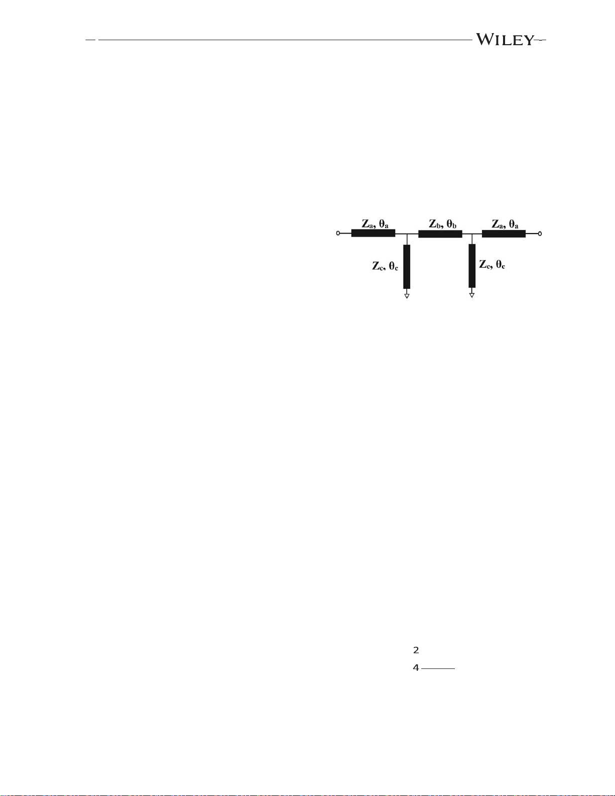
The proposed configuration of tri-frequency transmission line
Synthetic transmission lines have been employed to design a
model is presented in Figure 1. Two series transmission lines
dual-band RRC with harmonic suppression.6 In Refs. [7,8], a
of same characteristic impedance Z
dual-frequency RRC with enhanced bandwidth has been a and electrical length ua
are connected to both the ends of a p-shaped network. The p-
developed based on the T-shaped stepped impedance model.
shaped transmission line model is constructed
A dual-frequency phase shifter and combination of arbitrary
length microstrip line have been applied to design a dual-
band 180-degree RRC.9 In Ref. [10], the coupled line sections
have been employed to device a dualfrequency RRC. A
conventional hybrid with an additional stunt stub,11 3 section
transmission line12 and stepped impedance13 have been used
for realization of dual-band RRC with arbitrary power
division. The p-shaped unit with resonators has been used for
FIGURE 1 The configuration of the proposed tri-band transmission
the tri-frequency RRC design.14 Recently, some techniques line
have been reported for tri/quad-band operation such as
concentric dual split ring slots,15 cross-shaped with a shunt
with a series transmission line of characteristic impedance Zb
stub,16 extended Pi-shaped coupled line,17 and modified H-
and electrical length ub are tapped with 2 short-ended stubs at
shaped.18 This techniques can be employed for the realization
the bilateral-ends. The short-ended stub has characteristic
multiband microwave circuits such as power divider, branch
impedance of Zc and electrical length of uc. The proposed
line balun and hybrid couplers. Several attempts have been
topology is desired to be an equivalent unit for a quarter-wave
made in the past to address the issue of design of multiband
transmission line at all the 3 operating frequencies f1, f2, and
components. However, the development of a tri-band 180-
fc to design a tri-band 180-degree directional coupler. Here, fc
degree RRC with spurious bands suppression is yet to be
is the mean of the 2 arbitrarily chosen frequencies f1 and f2. explored.
The proposed tri-band transmission line model at fc is chosen
In this article, a complete analytical design procedure is
to have electrical lengths ua (fc), ub (fc), and uc (fc) as k/4, k,
described to develop a tri-band 180-degree hybrid coupler. A
and k/2 respectively. At f1, ua (f1), ub (f1), and uc (f1) are mk/4,
tri-frequency structure consists of p-shaped microstrip with 2
mk, and mk/2 respectively, where m5 f1/fc. Hence, the
series transmission lines at the bilateral ends is employed to
proposed transmission line is modeled as a quarter
design a tri-band coupler. This tri-frequency equivalent unit
wavelength line of characteristic impedance Za and electrical
is applied to replace each transmission line of the traditional
length 3k/2. The ABCD of the central p-shaped transmission
coupler. The design parameters are calculated from the
line in the proposed configuration can be computed as
simplified formulas derived using ABCD matrix method and
its graphical solutions. For validation, a tri-frequency A B
directional coupler is designed, fabricated, and tested for " # 5KLK; (1)
Global System for Mobile communication (GSM) (1.8 GHz),
Worldwide Interoperability for Microwave Access (WiMAX)
(3.5 GHz), and wireless local area network (WLAN) (5.2 C D p2network where
GHz) applications. With the tri-band operation, the proposed 1 0
coupler also provides spurious suppression by a level better
than 15 dB. The simulated and tested performances are well K52jcotuc 3; matched. (2) 1 Zc 5 cosub jZbsinub lOMoAR cPSD| 59256994 1614 | BARIK ET AL . L52 jZb 3: (3) sinub b 5 " A T
BT2cosðp=22T2uaðfaÞÞ jZTsinðp=222uaðfaÞ375 cosu
The coefficients of the ABCD matrix presented in (11) Equation 1 are given as
Equating Equations 1 and 10 we obtain, Z Z cos A5D5cosub1 (4) Zb5 a ðmp=2Þ; (12) bcotucsinub ; sinðmpÞ Zc B5jZ
Zc5 b ðmpÞcotðkp=2Þ: Z sin bsinub; (5) (13) 5 jZ : C5jsinub
22jcotuccosub 2jZbcot 2u2csinub : (6) CTDT p2network 64 sin
ðp=222uaðfaÞcosðp=222uaðfaÞ Zb Zc Zc
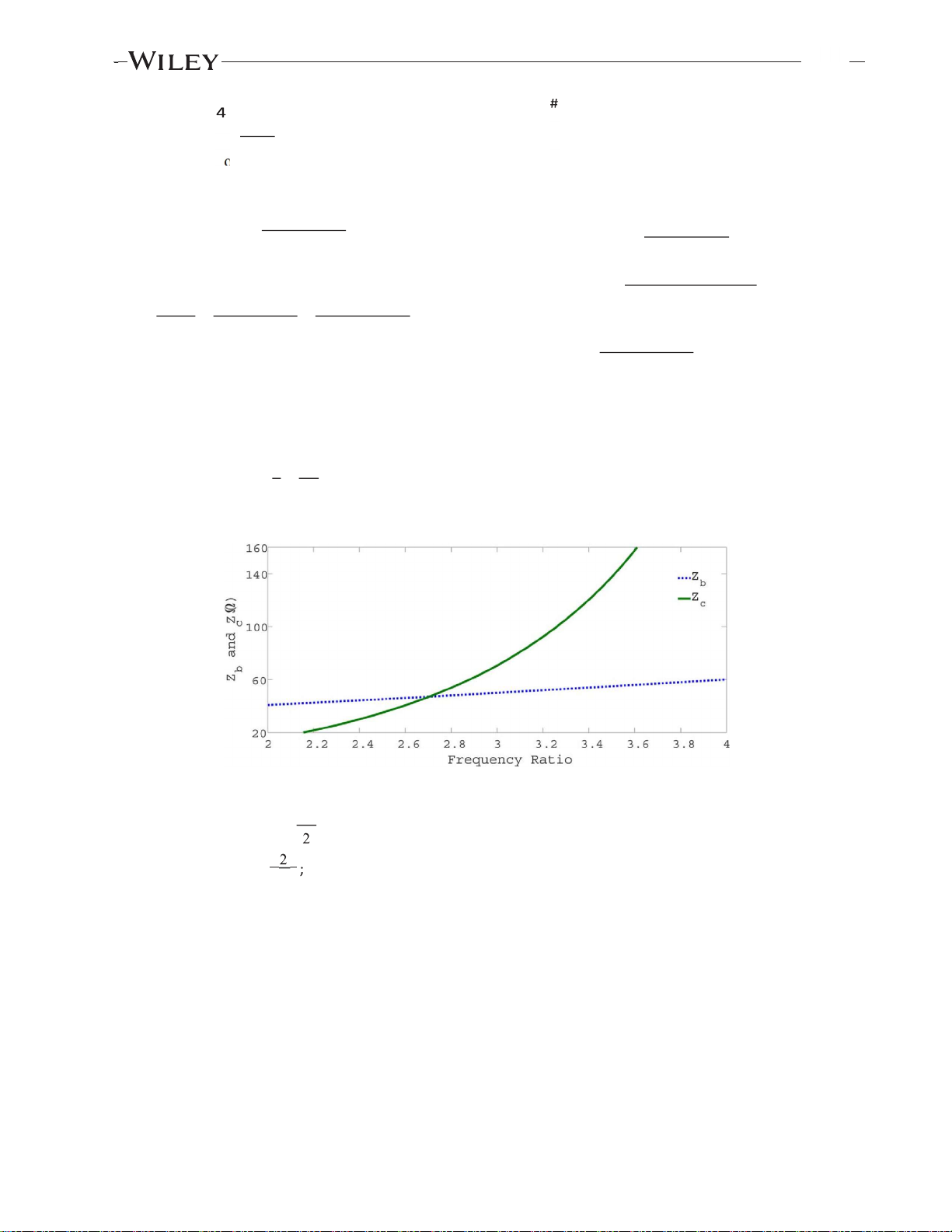
As fc is the mean frequency of f1 and f2, we can say
f252fc2f1. The electrical lengths at f2 are derived as follows: p mp uaðf2Þ5 2 ; (7) 2 4 u sinðkp=2Þ2cosðkpÞ bðf2Þ52p2mp; (8)
FIGURE 2 Design curve for Zb and Zc as a function of frequency ratio (f2/f1) [Color figure can be viewed at wileyonlinelibrary.com] mp
Based on the above study, a simple design guideline to ucðf2Þ5p2
develop a tri-frequency 3-dB rat-race coupler is briefed as ; follows: (9)
a. Select 2 operating frequencies f1 and f2 arbitrarily, and the
third operating frequency (fc) is calculated as the mean m5(10) of f1 and f2. 11r
b. After the selection of desired operating frequencies, where r5f theelectrical lengths (u 2/f1.
a, ub, and uc) can be computed
Since the proposed tri-band transmission line is an using Equations 7–9.
equivalent model of a quarter-wavelength transmission line
c. For tri-band operation, the characteristic impedance (Za)
with characteristic impedance Za, the ABCD matrix of the
and electrical length (ua) of the series transmission line
centrally placed p-shaped transmission line in the proposed
connected at both ends of the p-shaped network are topology can be expressed as
considered as 70.7 X and 458, respectively.
d. Based on the above calculation, the values Zb and Zc are
calculated using Equations 12 and 13, respectively. lOMoAR cPSD| 59256994 BARIK ET AL . | 1615
e. Using a microstrip line calculator, the physical dimen-
Zc versus frequency ratios. This graphical plot provides a
sions are calculated at the first operating frequency fc.
unique solution for a particular frequency ratio. Therefore,
the 2 operating frequencies (f1 and f2) can be calculated
Equations 11 and 12 are solved graphically to compute Zb and
arbitrarily and the third operating frequency (fc) is computed
Zc, respectively. The values of Za and ua are chosen as 70.7 X
as the mean of f1 and f2. Considering the fabrication limits (20
and 458, respectively. Figure 2 depicts the variation of Zb and
X to 150 X) of microstrip technology for RT/
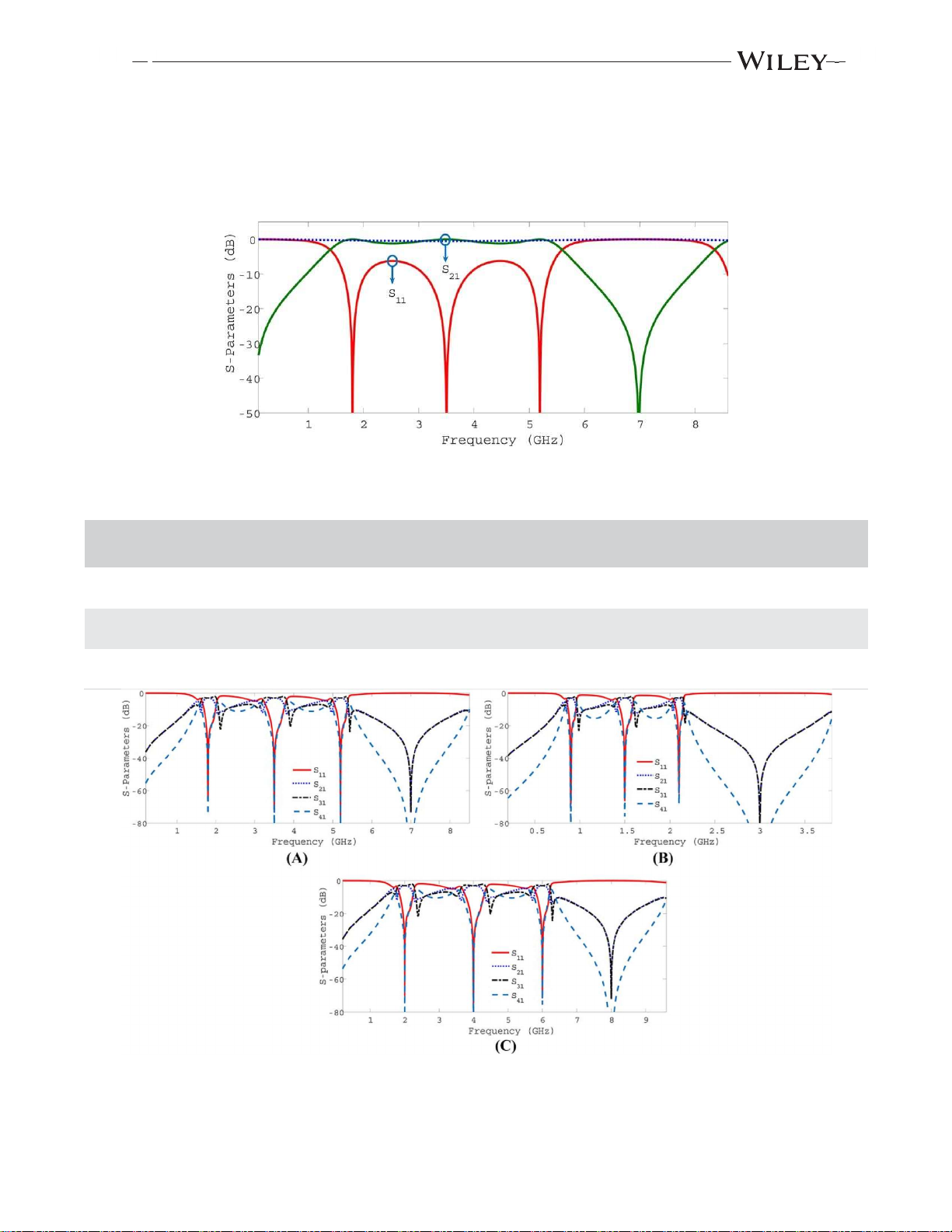
FIGURE 3 Calculated S-parameters of the quarter-wavelength transmission line (70.7 X) and the proposed tri-band transmissionline model [Color
figure can be viewed at wileyonlinelibrary.com] TABLE 1
Suitability of the proposed 180-degree rat-race coupler for various tri-band applications Designs Operating frequencies (GHz) Applications Za (X) Zb (X) Zc (X) Case 1 1.8/3.5/5.2 GSM/WiMAX/WLAN 70.7 48.9 60.85 Case 2 0.9/1.5/2.1 GSM/GPS/LTE 70.7 43.69 27.0 Case 3 2.0/4.0/6.0
Satellite communication (L/S/C Bands) 70.7 49.99 70.7
FIGURE 4 Circuit simulated S-parameters of the proposed tri-band coupler. (A) Case 1, (B) Case 2 and (C) Case 3 [Color figure can be viewed at wileyonlinelibrary.com]
Duroid 5870 substrate, the frequency ratio can be chosen
as 2.17other parameters for a frequency ratio of 2.89 are 1616 | BARIK ET AL . lOMoAR cPSD| 59256994
computed as: Zb 548.9 X, Zc 560.85 X ub 51808 and uc 5908. Using
these parameters, Figure 3 shows the S-parameters of the 70.7 X
line (solid line) and its equivalent tri-band model (dotted line).
The proposed structure exhibits similar properties as that of
traditional transmission line at 3 different operating frequencies.
As a result of the transmission zero created at 7 GHz, a stop band
response is extended up to at least 2fc. Hence, the proposed
transmission line model with trifrequency capability and
integrated stop-band response is a fascinating concept worthy for
the design of tri-band passive devices such as hybrid couplers,
power dividers, branch line balun and matching networks. 3 | D E S I G N O F T H E
T R I - F R E Q U E N C Y1 8 0 - D E G R E E H Y B R I DC O U P L E R
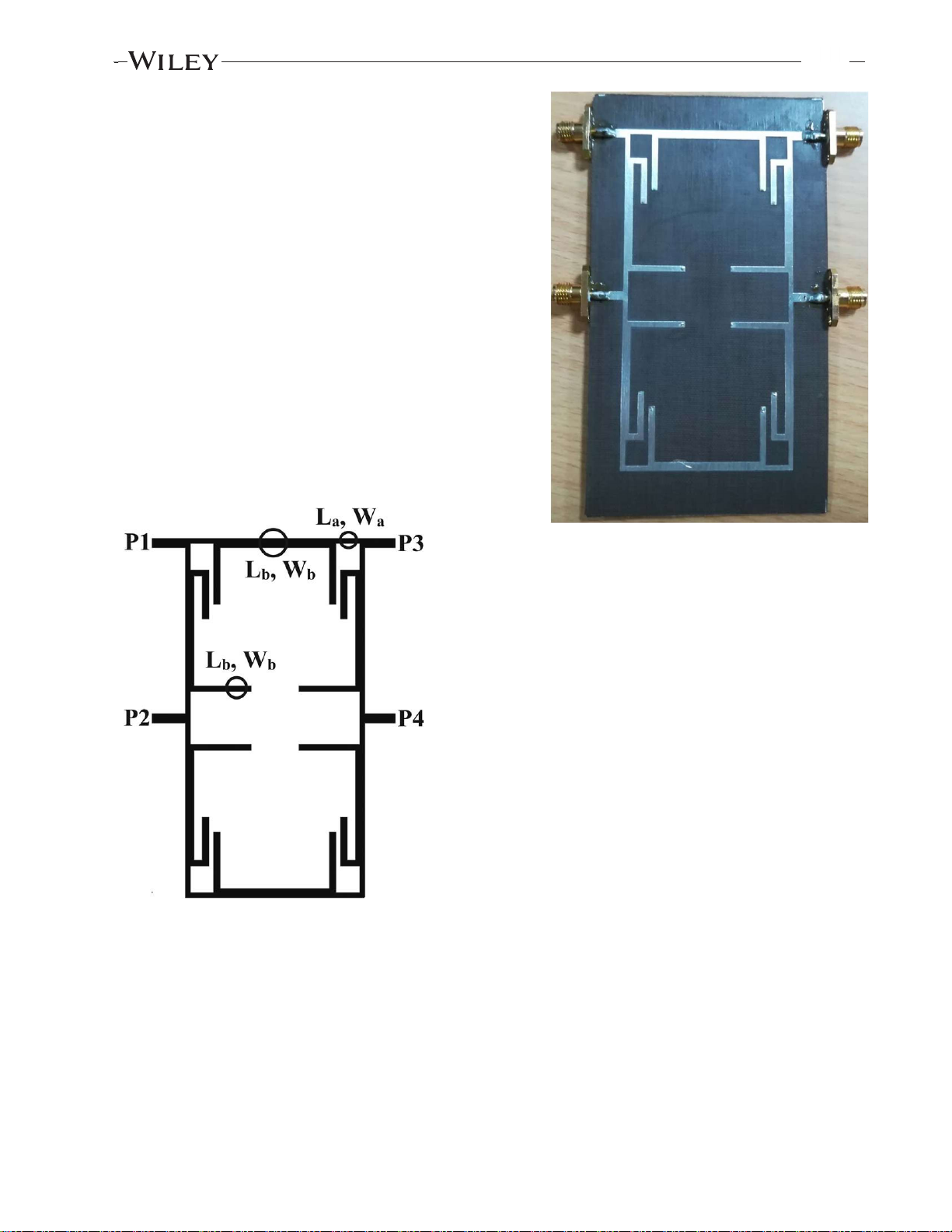
The traditional 180-degree hybrid coupler [21] is composed of 6
quarter-wavelength transmission lines with characteristic
FIGURE 6 Fabricated prototype of the tri-band 180-degree
directional coupler [Color figure can be viewed at wileyonlinelibrary.com]
impedance of 70.7 X. The proposed tri-frequency
structure is used to replace each transmission line of the
conventional coupler. In this section, 3 tri-band couplers
are designed for different set of applications. The
required impedances are calculated using Equations 11
and 12. The design parameters for different examples are
computed and illustrated in Table 1. The simulated
scattering parameters for different examples are depicted
in Figure 4. From the figure, it is seen that the matching
and isolation are well below 20 dB in each example at
all the operating frequencies. Also, it is observed that the
proposed design produces significant amount of
bandwidth at each operating frequency, which increases
the usability of the proposed coupler in the design of the
FIGURE 5 Layout of the final prototype with dimensions:
multiband systems. Also, it can be seen that the spurious
La57.76 mm, Wa51.3 mm, Lb530.46 mm, Wb52.39 mm, Lc515.4 mm and
bands beyond the third operating frequency are Wc51.69 mm
suppressed by the proposed structure.
Therefore, the tri-band transmission line provides
flexible solutions for different operating frequencies and
can be used to implement other microwave devices such
as branch line coupler, branch line balun, power
dividers, and matching network for amplifiers.
4 | F A B R I C A T I O NA N D BARIK ET AL . | 1617 lOMoAR cPSD| 59256994 M E A S U R E M E N TO FT H E
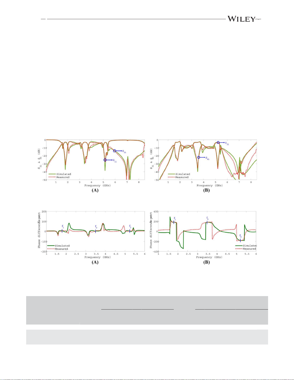
360.5 dB at each operating frequencies. Measurement P R O T O T Y P E
result illustrates that the bandwidths of 15 dB matching
and isolation are more than 220 MHz at all the working
To validate the design analysis, a tri-frequency 180-degree hybrid
frequencies. The bandwidths measured over amplitude
coupler (Case-3) operating at 1.8/3.5/5.2 GHz is simulated and
imbalance (061 dB) at sum and difference port excitation
fabricated to cover the GSM/WiMAX/WLAN applications. The
are larger than 150 and 190 MHz, respectively. Figure 8
final layout with dimensions is shown in Figure 5. Rogers
depicts the phase difference of the proposed prototype at
RT/Duroid 5870 substrate with Er 52.33 and thickness of 0.787
ports 1 and 4 excitations. The bandwidths measured over
mm is used to fabricating the coupler based on microstrip
phase imbalance at sum (08658) and difference
technology. The fabricated prototype is depicted in Figure 6 and
(1808658) ports excitations are larger than 200 MHz at
it is measured using the Rohde & Schwarz ZVL network analyzer.
each working frequencies. The simulated and tested
The full-wave simulated and measured frequency responses are
performances of the proposed tri-band hybrid coupler
shown in Figures 7 and 8. It is observed that the performances
are illustrated in Table 2. The bandwidths for input
obtained using full-wave simulator is very similar to the measured
matching, isolation, amplitude, and phase imbalances
results. Input matching (S11 and S44) and isolation are more than
are calculated and listed in Table 3. In addition, the
20 dB at all the 3 operating frequencies at sum and difference port
proposed tri-frequency equivalent model
excitation. Insertion loss at sum and difference port is maintaining
FIGURE 7 Simulated and measured frequency variation of S-parameters for the sum port excitation. (A) S11 and S21. (B) S31 and S41 [Color figure
can be viewed at wileyonlinelibrary.com]
FIGURE 8 Simulated and measured frequency variation of phase difference. (A) For sum port excitation. (B) For difference port excitation [Color
figure can be viewed at wileyonlinelibrary.com] TABLE 2
Experimental performance of the tri-band 180-degree directional coupler Full-wave simulated (d B) Measured (dB) Parameters @ f1 @ f2 @ f3 @ f1 @ f2 @ f3 Matching (S11) 37.28 22.67 28.01 28.64 29.41 25.61 Isolation (S41) 24.94 39.79 34.54 26.32 35.05 36.24 1618 | BARIK ET AL . lOMoAR cPSD| 59256994 Insertion loss (S21) 3.14 3.04 3.22 2.85 3.05 3.22 Insertion loss (S31) 3.22 3.28 3.57 3.10 3.14 3.60 5.18 1.538 4.08 2.958 3.018 3.18 Phase difference (/S312/S21) Matching (S44) 28.8 25.29 27.28 24.79 26.41 29.38 Isolation (S14) 24.59 31.44 30.19 26.31 27.1 30.5 Insertion loss (S24) 3.62 3.57 3.86 3.25 3.65 3.91 Insertion loss (S34) 3.28 3.43 3.62 3.73 3.85 3.10 1838 1808 181.38 1828 1818 1818 Phase difference (/S342/S24)
produces a transmission zero at 7 GHz. As a result of this Table 4 shows the performance comparison between the proinherent
property, spurious band response beyond the operat- posed tri-band RRC and the previously reported tri-band ing frequencies
is suppressed by a level more than 20 dB. RRC. TABLE 3
Bandwidth comparison of the proposed tri-band hybrid coupler Full-wave simulated ( MHz) Measured (MHz) Characteristic parameters @ f1 @ f2 @ f3 @ f1 @ f2 @ f3 15-dB matching (S11) 250 380 260 240 350 250 220 230 310 230 220 310 15-dB matching (S44)
15-dB Isolation for sum (R) and 340 410 260 330 420 260
difference (D) port excitation
61.0 dB DA for R-port excitation 150 250 190 160 240 200 668 DU for R-port excitation 300 300 190 320 260 200
61.0 dB DA for D-port excitation 200 280 200 210 260 190 668 DU for D-port excitation 200 220 250 220 280 260
f151.8 GHz, f253.5 GHz, f355.2 GHz, R: Sum, D: Difference, DA5Amplitude imbalance and DU5Phase imbalance. TABLE 4
Comparison between the proposed work and previously reported tri-band RRC f 1/f2/f3 Input matching Isolation Spurious Advantages/ Ref. Methods (GHz) (dB) (dB) suppression limitations Ref. [14] Resonators 1.0/1.5/2.5 9.95/19.2/12.5 36.1/28.2/29.2 Not reported Needs additional lumped elements BARIK ET AL . | 1619 lOMoAR cPSD| 59256994 This Work Extended p- 1.8/3.5/5.2 28.6/29.4/25.6 26.3/35/36.2 Beyond the third Does not require any shaped model frequency band lumped elements, easily fabricatable, spurious band suppression 5 | C O N C L U S I O N
[6] Chen C-C, Sim C, Wu Y-J. Miniaturised dual-band rat-race coupler
with harmonic suppression using synthetic transmission line.
In this article, a tri-frequency 180-degree hybrid coupler with
Electron Lett. 2016;52(21):1784–1786.
spurious suppression has been presented. The proposed
[7] Bekasiewicz A, Koziel S, Zieniutycz W. A structure and design
coupler has been implemented using a tri-band extended p-
optimization of novel compact microstrip dual-band rat-race
shaped model. The essential design equations are obtained
coupler with enhanced bandwidth. Microwave Opt Technol Lett.
using ABCD matrix method and simplified through graphical 2016;58(10):2287–2291.
plots to compute circuit parameters. To validate the design
[8] Bekasiewicz A, Koziel S, Zieniutycz W. On design optimization of
approach, a tri-band 180-degree hybrid coupler working at
miniaturized microscrip dual-band rat-race coupler with enhanced
1.8/3.5/5.2 GHz is designed, fabricated, and tested. The
bandwidth. In: 21st International Conference on Microwave, Radar
bandwidths of isolation, matching, amplitude and phase
and Wireless Communications (MIKON); 2016: 1–4.
imbalances are calculated. In addition to tri-band response,
[9] Arigong B, Shao J, Zhou M, et al. An improved design of dualband
the spurious bands beyond the operating frequencies have
3 db 180 directional coupler. Prog Electromagn Res C.
been suppressed by a level better than 15 dB. Therefore, the 2015;56:153–162.,
application of the proposed structure in the design of
[10] Corrales E, Baldomero A, de Paco P. A dual-band 180-degree
impedance matching, power divider, and branch line balun
hybrid coupler based on coupled-line sections. IEEE Microwave
will be an attractive concept for the future investigation.
Wireless Compon Lett. 2015;25(4):211–213.
[11] He Q, Shen J, Liu Q, Li J, Liang L. A simplified dual-band ratrace ORCID
hybrid for arbitrary power division ratio with only single shunt
stub. J Electromagn Waves Appl. 2013;27(16): 2101–2109. Rusan Kumar Barik
http://orcid.org/0000-0001-7691- 2485
[12] Zhang L-Z, Zhou L, Jiang W. A compact dual-band coupler with
arbitrary power dividing ratio using broadsidecoupled microstrip.
J Electromagn Waves Appl. 2013;27(2):140– 148. REFERENCES
[13] Wu LS, Mao J, Yin WY. Miniaturization of rat-race coupler with
[1] Liao Z-H, Zhang X-C, Yang X. Compact reconfigurable rat-race
dual-band arbitrary power divisions based on steppedimpedance
coupler with tunable frequency and tunable power dividing ratio.
double-sided parallel-strip line. IEEE Trans Compon Packag
Int J RF Microwave Comput-Aided Eng. 2017;27(9):e21139–
Manuf Technol. 2012;2(12):2017–2030. e21138.
[14] Wang Z, Jang JS, Park CW. Tri-band rat-race coupler using
[2] Phani Kumar KV, Karthikeyan SS. Highly compact wideband
resonators. In: IEEE International Conference on Microwave
double-section rat-race hybrid with harmonic suppression using
Technology Computational Electromagnetics; 2011: 186–189.
series and shunt stepped impedance transmission lines. Int J
[15] Velan S, Kingsly S, Kanagasabai M, Alsath MGN, Selvam YP,
Microwave Wireless Technol. 2017;9(04):797–803.
Subbaraj S. Quad-band rat-race coupler with suppression of
[3] Kumar KVP, Barik RK, Krishna IS, Karthikeyan SS. Design of
spurious pass bands. IEEE Microwave Wireless Compon Lett.
compact 1808 hybrid coupler for unequal power division ratio 2016; 26(7):490–492.
using slow wave structures. In: Twenty-third National Conference
[16] Barik RK, Karthikeyan SS. Design of dual/tri-frequency
on Communications (NCC); 2017: 1–5.
impedance transformer with ultra-high transforming ratio. Int J
[4] Tseng CH, Mou CH, Lin CC, Chao CH. Design of microwave dual-
Microwave Wireless Technol. 2017; 9:1951–1960.
band rat-race couplers in printed-circuit board and GIPD
technologies. IEEE Trans Compon Packag Manuf Technol. 2016;6(2):262–271.
[5] Hsu CL, Kuo JT, Chang CW. Miniaturized dual-band hybrid
couplers with arbitrary power division ratios. IEEE Trans
Microwave Theory Tech. 2009;57(1):149–156. lOMoAR cPSD| 59256994 | 1620 SUH AND JEON
at the common node of the differential pair while the carrier
is simultaneously suppressed. The ED is fabricated in a
[17] Barik RK, Karthikeyan SS. A novel design of ultra-high impedance
low-cost 65-nm bulk CMOS technology. The measured
transforming ratio quad-band matching network. Microwave Opt
average responsivity and noise equivalent power are 1.16
Technol Lett. 2017;59(8):2021–2026.
kV/W and 234 pW/Hz1/2, respectively, from 110 to 170
GHz. To demonstrate its high-speed demodulation
[18] Barik RK, Karthikeyan S. A novel quad-band impedance
capability, the ED is employed as an OOK receiver along
transformer with ultra-high transforming ratio. AEU Int J Electron Commun. 2017;78:157–161.
with an on-chip D-band amplifier. The receiver
demodulates the OOK signal of up to 4 Gbps through the
[19] Pozar DM. Microwave Engineering. New York: Wiley; 2005.
air channel over a distance of 0.11 m. Furthermore, an
[20] Balanis CA. Antenna Theory: Analysis and Design. Hoboken, NJ:
airchannel transfer of high-definition video signal Wiley-Interscience; 2005.
complying with the SMPTE 292M standard is successfully
demonstrated using the receiver.
How to cite this article: Barik RK, Krishna IS,
K E Y W O R D S envelope detector, full D-band, OOK
Karthikeyan SS. Design of a tri-band 180-degree communication
directional coupler with spurious suppression based on
extended pi-shaped microstrip line. Microw Opt Technol Lett. 2018;60:1612–1619.
https://doi.org/10.1002/ mop.31213 1 | I N T R O D U C T I O N Received: 21 November 2017
Recently, the D-band spectrum (110–170 GHz) has attracted DOI: 10.1002/mop.31212
considerable attention for ultra-high-speed wireless
communication due to its widely available bandwidth. As the A full D-band CMOS envelope
airchannel loss is relatively high, short-range communication
based on a simple modulation scheme such as on-off-keying detector for high-speed OOK
(OOK) is promising at the D-band.
As the transistor scaling technology advances, it becomes wireless communication
feasible to implement integrated circuits and systems using
silicon-based processes at the D-band.1 However, the highly Bohee Suh | Sanggeun Jeon
scaled advanced CMOS processes such as 28-nm or 40-nm
nodes and silicon-on-insulator technologies suffer from high
School of Electrical Engineering, Korea University, Anam-dong,
manufacture cost and limited accessibility. Abundant analog
Seongbuk-gu, Seoul 136-713, Korea
and digital integrated systems are still implemented using Correspondence
less-scaled and low-cost CMOS processes. To maximize the
Sanggeun Jeon, School of Electrical Engineering, Korea
integrability with the systems, the D-band high-speed
University, Anam-dong, Seongbuk-gu, Seoul 136-713, Korea. Email: sgjeon@korea.ac.kr
communication circuit should also be implemented using the less-scaled process.2–4 Funding information
Defensive Specialized Laboratory for Terahertz Electronic Devices through
In this article, a wideband envelope detector (ED) for a
the Korea Agency for Defense Development, Grant/Award Number:
D-band OOK receiver is presented. The chip is fabricated in UD150043RD
a low-cost 65-nm bulk CMOS process. The design of the ED
is discussed, followed by measurement results of the Abstract
responsivity and noise equivalent power (NEP). Also, the
This article presents a D-band CMOS envelope detector
OOK demodulation capability of the ED is demonstrated by
(ED) used for a wideband on-off-keying (OOK) receiver.
transferring PRBS and high-definition (HD) video signal
The ED consists of an input balun and a differential through the air channel.
common-source pair. The input balun is designed in a low-
loss rat-race coupler. The baseband output signal is taken lOMoAR cPSD| 59256994 | 1621
2 | D E S I G N O F D - B A N D
E N V E L O P ED E T E C T O R
The schematic of the ED is shown in Figure 1. The transistor
fMAX of the 65-nm bulk CMOS process is 210 GHz, which is
not high enough to design D-band circuits. Therefore, a
conventional differential common-source topology (M1, M2)
is adopted for reliable envelope-detecting operation. The DC
output is taken at the common output node of the differential
pair, so that the RF signal is suppressed by 39.3 dB based on
simulation without any additional filter.
Tài liệu liên quan:
-

Cấu trúc dữ liệu và giải thuật: Mối quan hệ và Lập trình C | Học viện Kỹ thuận Quân sự
578 289 -

Shell programming exercises in Linux | Học viện Kỹ thuận Quân sự
75 38 -

Lập Trình Nhân Linux - Phần 1: Lab 3 và Tạo Makefile | Học viện Kỹ thuận Quân sự
101 51 -

Lab 1: Thực hiện lệnh Shell trên Linux | Học viện Kỹ thuận Quân sự
61 31 -

Khái niệm và phân tích Bus máy tính: Giai đoạn tăng trưởng và phát triển | Học viện Kỹ thuận Quân sự
73 37