Báo cáo thí nghiệm "Lab 4 Report" môn Mạch điện tử nội dung bằng tiếng Anh | Đại học Bách khoa Thành phố Hồ Chí Minh
Báo cáo thí nghiệm "Lab 4 Report" môn Mạch điện tử nội dung bằng tiếng Anh của Đại học Bách khoa Thành phố Hồ Chí Minh với những kiến thức và thông tin bổ ích giúp sinh viên tham khảo, ôn luyện và phục vụ nhu cầu học tập của mình cụ thể là có định hướng ôn tập, nắm vững kiến thức môn học và làm bài tốt trong những bài kiểm tra, bài tiểu luận, bài tập kết thúc học phần, từ đó học tập tốt và có kết quả cao cũng như có thể vận dụng tốt những kiến thức mình đã học vào thực tiễn cuộc sống. Mời bạn đọc đón xem!
Môn: Mạch điện tử (EE2035) 5 tài liệu
Trường: Trường Đại học Bách khoa - Đại học Quốc gia Thành phố Hồ Chí Minh 721 tài liệu
Tác giả:
Preview text:
lOMoARcPSD| 36991220 1 Introduction
Altium Designer is an electronic design automation software
package for printed circuit board (PCB), FPGA and embedded
software design, and associated library and release management
automation. A Printed Circuit Board (PCB) mechanically supports
and electrically connects electric components using conductive
tracks, pads and other features etched from copper sheets laminated
onto a non-conductive substrate.
Figure 1.1: PCB circuit in Altium Designer
In this lab, two different voltage regular circuits are designed in
Altium, based on IC 7805 and LM2596. The manuals are provided by videos.
2 Voltage Regulator using 7805
Voltage regulator like IC7805 belongs to the 78xx series ICs. In the
78xx series, xx represents the fixed output voltage value and 7805 is
a fixed linear voltage regulator. Batteries provide a voltage of 1.2V,
3.7V, 9V, and 12V. This voltage is good for the circuits which volt
age requirements are in that range. The regulated power supply in this regulator is +5V DC.
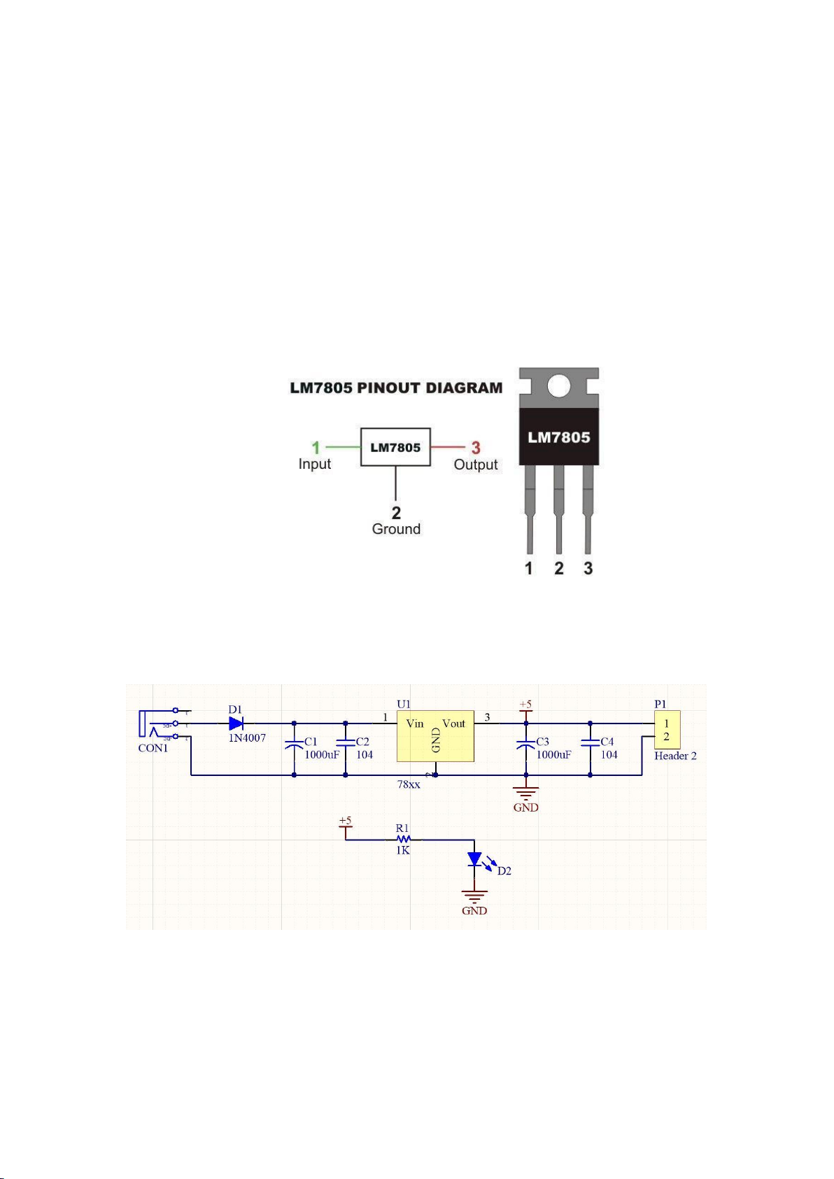
The 7805 voltage regulator is a three-terminal voltage regulator IC. In
various applications, a 7805 voltage regulator with a fixed output lOMoARcPSD| 36991220
voltage is used. The availability of this is through various packages
like SOT-223, TO-263, TO-220, and TO-3. Among this, TO-220 is
the most used one. The pin diagram of 7805 voltage regulator IC and
its description are explained bellow: •
Pin1 - Input: This is an input pin and the voltage
rangeshould be between 7V to 35V. an unregulated voltage is applied
to this input pin for regulation. The pin will receive its maximum efficiency at 7.2V input. •
Pin 2 - Ground: Pin2 is the ground pin, it means the
ground isconnected to this pin. Input and output are common to it.
Figure 1.2: LM7805 Pin Out •
Pin 3 - Output: Pin3 is the output pin, where the
regulatedoutput is taken by this pin. It is about 5V(4.8V to 5.2V)
Figure 1.3: Voltage regulator using 78xx schematic in Altium Designer
The basic circuit of 7805 is very simple. It just needs two capacitors
if the input is unregulated DC voltage, even the two capacitors used lOMoARcPSD| 36991220
are also not mandatory. This 7805 circuit is capable of upholding fixed
output voltage even if some changes take place in input voltage The
manual for this circuit is posted at the link bellow:
https://www.youtube.com/watch?v=mSEBrma5MNM
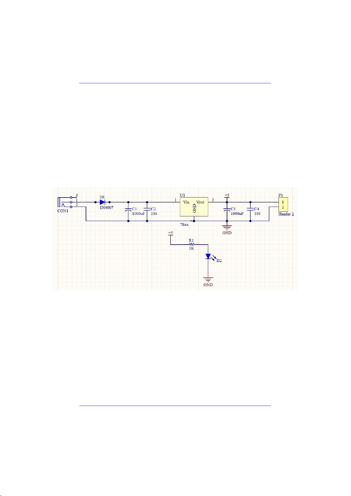
2.1 Schematic design
Students are proposed to capture the schematic design in Altium
Designer and place the image in this part.
Some hot keys are normally used in the schematic is the space bar, X(
horizontal mirror), Y (vertial mirror) and Ctrl + W (place a wire).
Your image goes here
The schematic design of Voltage regulator circuit using 7805 2.2 PCB layout
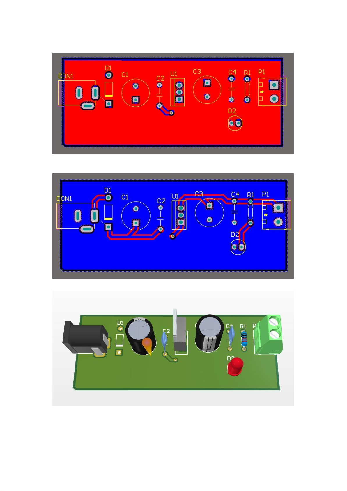
Similarly to the schematic, some snap shorts of for the TOP,
BOTTOM layers are required in this report. Moreover, several 3D
images of your schematic are also required.
A manual video can be found at:
https://www.youtube.com/watch?v=PW_QQpoODDk lOMoARcPSD| 36991220
Your image goes here
The top layer of the PCB layout
The bottom layer of the PCB layout
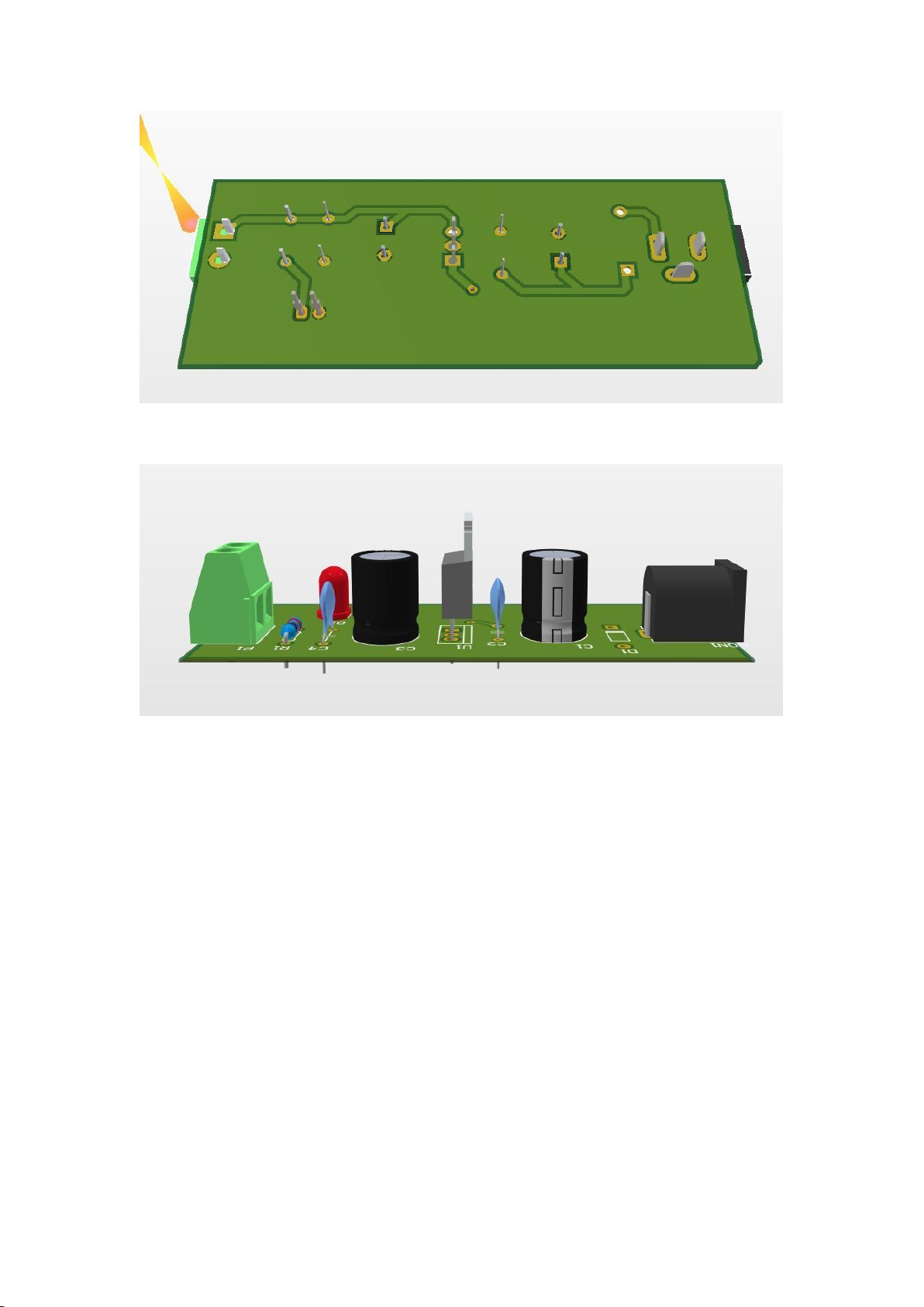
The top view of the circuit in 3D model lOMoARcPSD| 36991220
The bottom view of the circuit in 3D model
The voltage regulator circuit using 7805 in 3D
3 Volatage Regulator using LM2596
LM2596 is a voltage regulator mainly used to step down the voltage
or to drive load under 3A. It is also known as DC-to-DC power
converter or buck converter which is used to step down the voltage
from its input supply to the output load. The current goes up during
this voltage step down process.
LM2596 comes with a remarkable load and line regulation. It is
available in both versions: fixed output voltage version with 3.3V, 5V,
12V, and customized output version where you can choose the output
as per your requirement. This regulator is incorporated with a fixed-
frequency oscillator and an internal frequency compensation method. lOMoARcPSD| 36991220
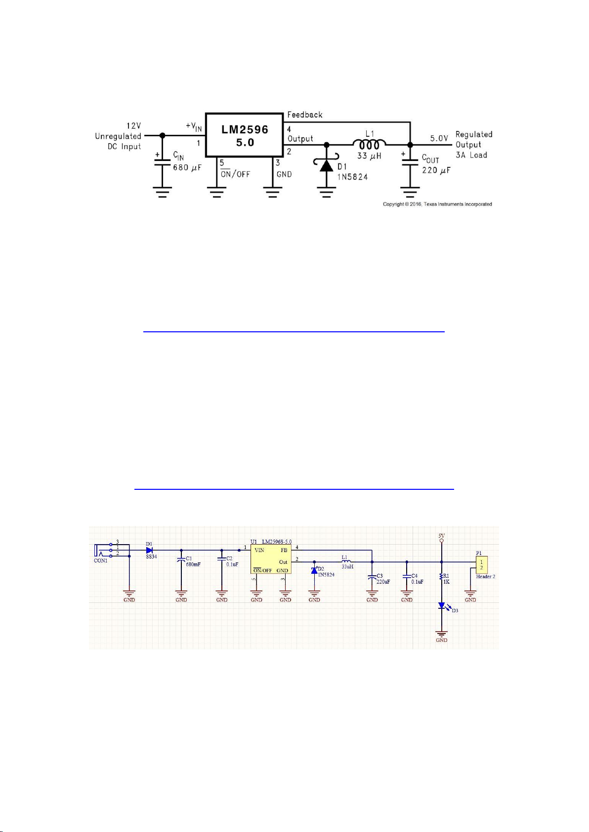
The typical connection for LM2596 is proposed by Texas Instrument (TI), as following:
Figure 1.4: Typical connection for LM2596
This circuit is simulated in PSpice in previous lab, and is implemented
in Altium Design in this lab. The introduction of this circuit is
presented in the video bellow:
https://www.youtube.com/watch?v=57Ra92p3C0k 3.1 Schematic design
Students are proposed to capture the schematic design in Altium
Designer and place the image in this part.
Some hot keys are normally used in the schematic is the space bar, X(
horizontal mirror), Y (vertial mirror) and Ctrl + W (place a wire).
The manual is posted in this link:
https://www.youtube.com/watch?v=DGiHsGWPyYw
Your image goes here
The schematic design of Voltage regulator circuit using LM2596 lOMoARcPSD| 36991220 3.2 PCB layout
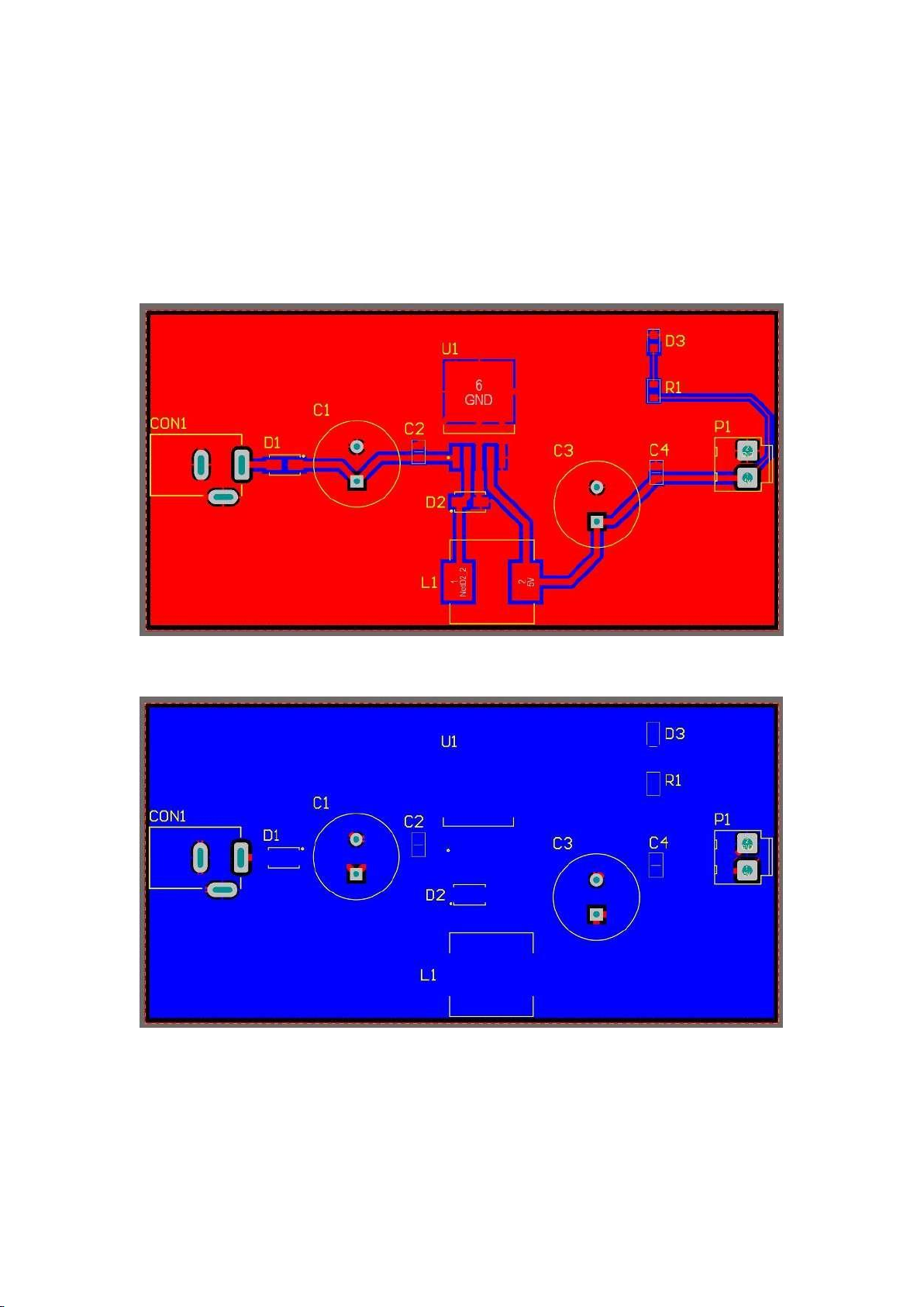
Similarly to the schematic, some snap shorts of for the TOP,
BOTTOM layers are required in this report. Moreover, several 3D
images of your schematic are also required.
Your image goes here
The top layer of the PCB layout
The top layer of the PCB layout lOMoARcPSD| 36991220
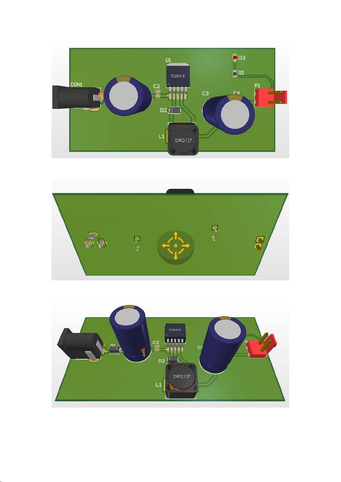
The top view of the circuit in 3D model
The bottom view of the circuit in 3D model.
The voltage regulator circuit using LM2596 in 3D