Báo cáo thí nghiệm "Lab 5 Report" môn Mạch điện tử nội dung bằng tiếng Anh | Đại học Bách khoa Thành phố Hồ Chí Minh
Báo cáo thí nghiệm "Lab 5 Report" môn Mạch điện tử nội dung bằng tiếng Anh của Đại học Bách khoa Thành phố Hồ Chí Minh với những kiến thức và thông tin bổ ích giúp sinh viên tham khảo, ôn luyện và phục vụ nhu cầu học tập của mình cụ thể là có định hướng ôn tập, nắm vững kiến thức môn học và làm bài tốt trong những bài kiểm tra, bài tiểu luận, bài tập kết thúc học phần, từ đó học tập tốt và có kết quả cao cũng như có thể vận dụng tốt những kiến thức mình đã học vào thực tiễn cuộc sống. Mời bạn đọc đón xem!
Môn: Mạch điện tử (EE2035) 5 tài liệu
Trường: Trường Đại học Bách khoa - Đại học Quốc gia Thành phố Hồ Chí Minh 721 tài liệu
Tác giả:

Preview text:
lOMoARcPSD| 36991220 1 Introduction
Operational Amplifiers, also known as Op-amps, are basically a voltage
amplifying device designed to be used with components like capacitors and
resistors, between its in/out terminals. They are essentially a core part of analog
devices. Feedback components like these are used to determine the operation of
the amplifier. The amplifier can perform many different operations, giving it the name Operational Amplifier.
One key to the usefulness of these little circuits is in the engineering principle of
feedback, particularly negative feedback, which constitutes the foundation of
almost all automatic control processes. The principles presented in this section,
extend well beyond the immediate scope of electronics. It is well worth the
electronics student’s time to learn these principles and learn them well.
Operational amplifiers can have either a closed-loop operation or an open-loop
operation. The operation (closed-loop or open-loop) is determined by whether or
not feedback is used. Without feedback the operational amplifier has an open-
loop operation. This open-loop operation is practical only when the operational
amplifier is used as a cooperator (a circuit which compares two input signals or
compares an input signal to some fixed level of voltage). As an amplifier, the
open-loop operation is not practical because the very high gain of the operational
amplifier creates poor stability. (Noise and other unwanted signals are amplified
so much in open-loop operation that the operational amplifier is usually not used
in this way.) Therefore, most operational amplifiers are used with feedback (closed-loop operation). 2 Closed Loop Operation
Operational amplifiers are used with degenerative (or negative) feedback which
reduces the gain of the operational amplifier but greatly increases the stability of
the circuit. In the closed-loop configuration, the output signal is applied back to
one of the input terminals. This feedback is always degenerative (negative). In
other words, the feedback signal always opposes the effects of the original input
signal. One result of degenerative feedback is that the inverting and noninverting
inputs to the operational amplifier will be kept at the same potential.
Closed-loop circuits can be of the inverting configuration or non-inverting configuration.
2.1 Non inverting configuration
The typical circuit for this configuration is shown in the figure bellow: lOMoARcPSD| 36991220
Figure 1.1: Non inverting configuration
The new component, named also OPAMP (Operational Amplifier) is easily
found in the favorite list of the PSPICE.
In order to explain the 4V at the output, it is obviously that V (+) = V (−) = 2V
in a closed loop configuration. Therefore, from a resistor bridge at the output, VOUT = 4V .
2.2 Inverting configuration
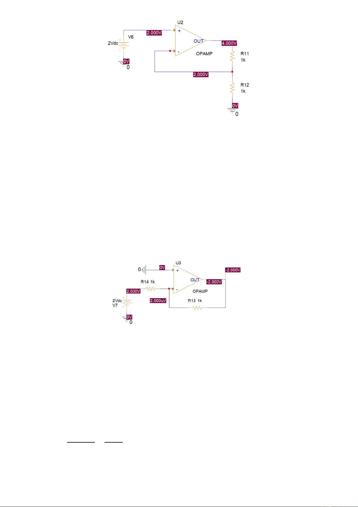
In this configuration, the output is connected directly to a pin of the opamp as follow:
Figure 1.2: Inverting configuration
As the output voltage is negative, which is inverted to the input, the name of this
circuit is the invert connection. Students are proposed to perform calculations to
confirm the output, which is −2V.
The circuit has negative feedback. So we can obtain that: (+) =(−) =0() 2−(−) 2−0 = = =2() 14 1000
(−) − = ×13 =2×10−3×1000=2() lOMoARcPSD| 36991220 => =−2() 3 Exercise and Report 3.1 Voltage Follower
Voltage follower is one of the simplest uses of an operational amplifier, where
the output voltage is exactly same as the input voltage applied to the circuit. In
other words, the gain of a voltage follower circuit is unity. The connections are proposed as follows:
Figure 1.3: Opamp follower circuit
A voltage follower has low output impedance and extremely high input
impedance, and this makes it a simple and effective solution to problematic
impedance relationships. If a high-output-impedance sub-circuit must transfer a
signal to a low-input-impedance sub-circuit, a voltage follower placed between
these two sub-circuits will ensure that the full voltage is delivered to the load.
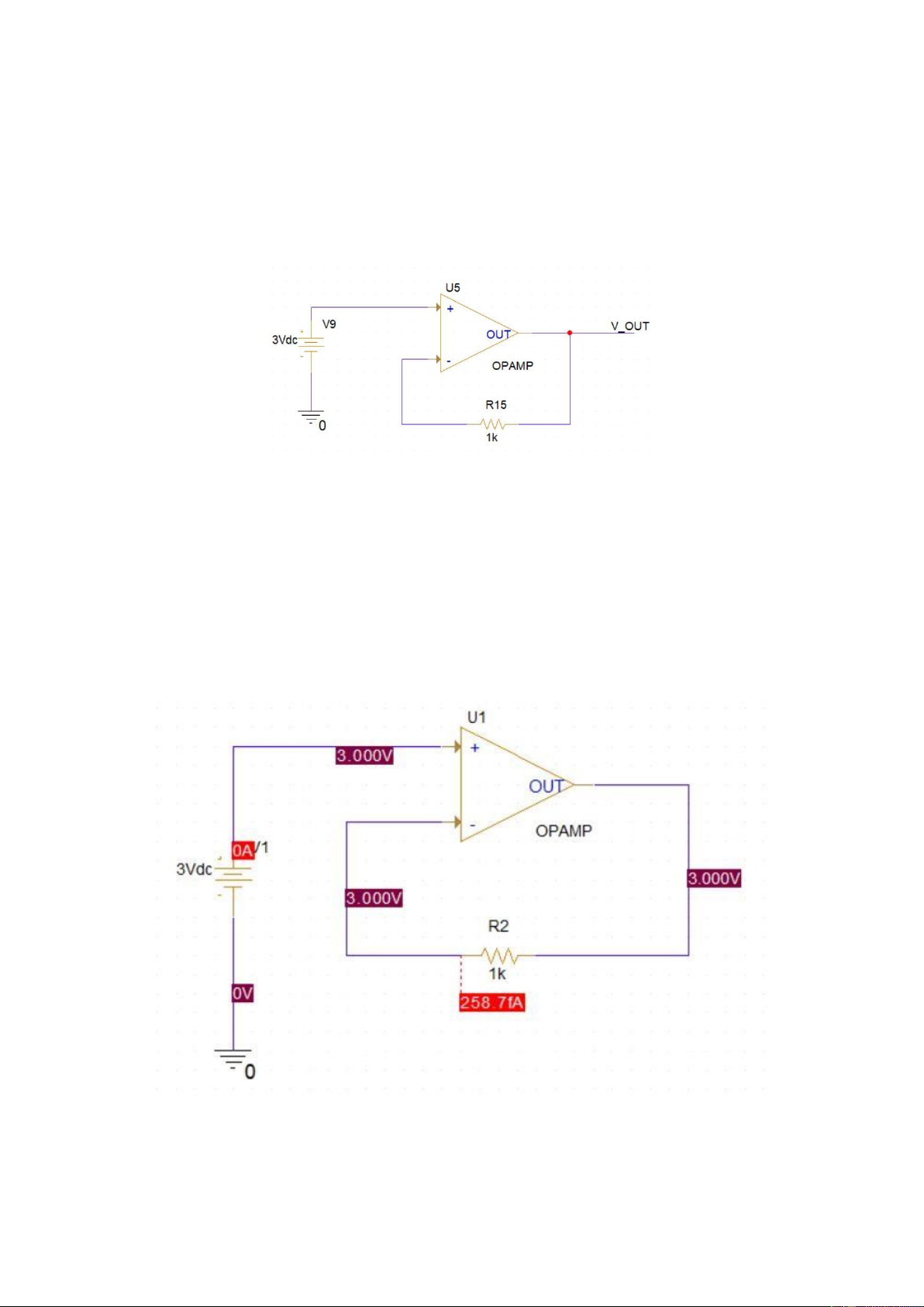
Students are propose to run the simulation with bias mode to confirm that
VOUT = V(+). The feedback resistance is also required to change. lOMoARcPSD| 36991220
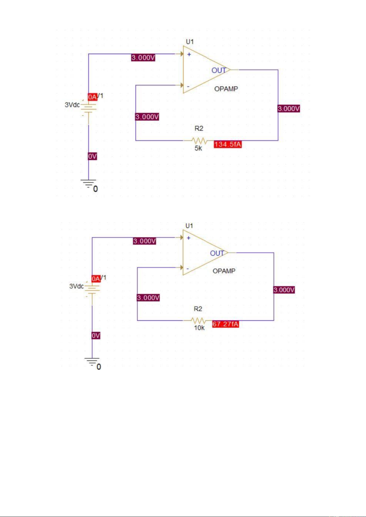
The bias point simulation when feedback resistance is 1k Ω
The bias point simulation when feedback resistance is 5k Ω
The bias point simulation when feedback resistance is 10k Ω
Your calculations are presented here to prove VOUT = V (+) with any value of R15.
In any case, whenever we change the value of R15, there is no current pass
through it. Thus we always have V(+) = V(−) = VOUT = 3(V )
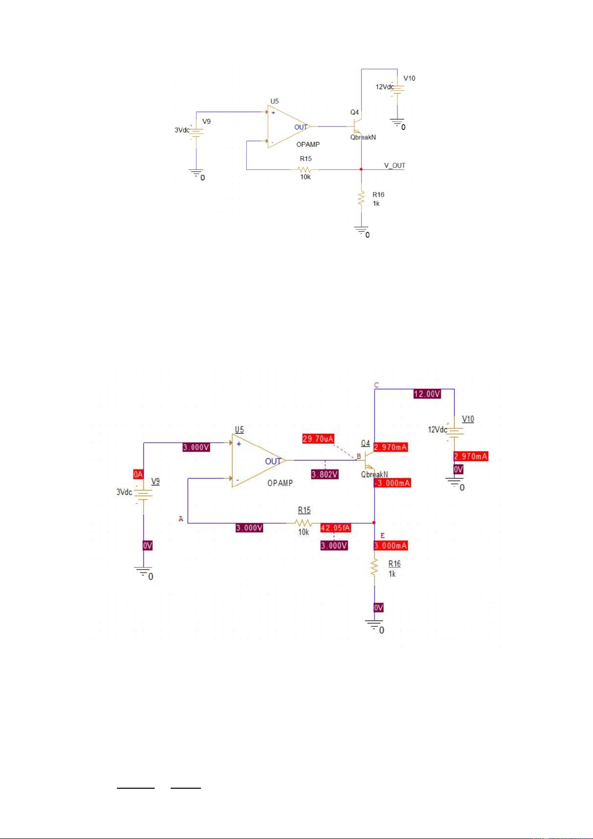
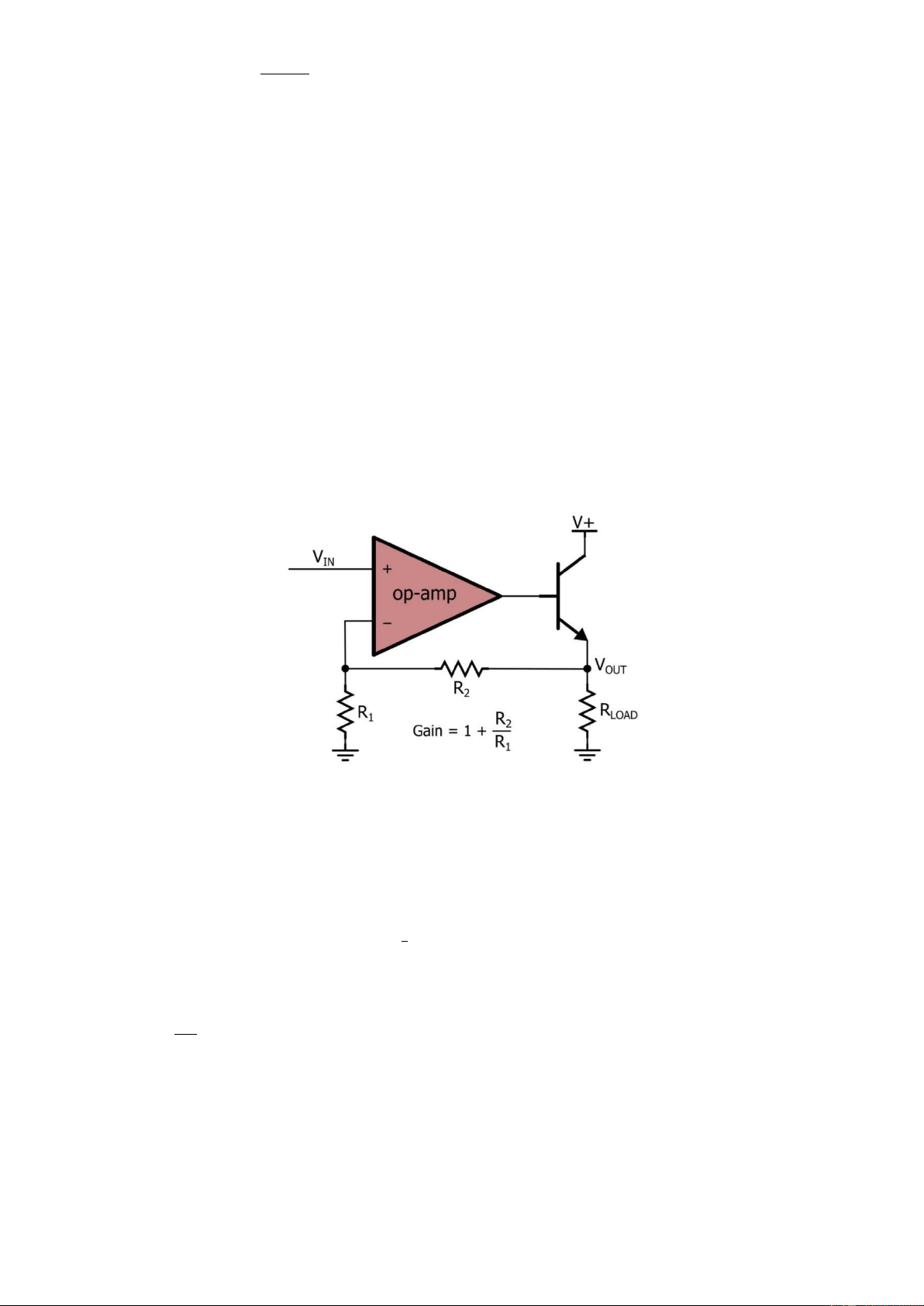
3.2 High-Current Voltage Follower
The voltage follower’s low output impedance makes it a good circuit for driving
current into a low-impedance load, but it’s important to remember that most op- lOMoARcPSD| 36991220
amps are not designed to deliver large output currents. The most basic circuit for
buffering an op-amp’s output current is the following:
Figure 1.4: Opamp follower circuit
The voltage at the positive pin of the Opamp is copied to VOUT . In this schematic,
R16 is used to simulate a load device, which can be a motor or an high power
LED. However, in this case, there is a high current can pass the load.
Students are proposed to run the simulation with bias configuration, capture the
results and place them in the report. The bias point simulation
Finally, your computations go here to explain the results.
Since there is no current pass through the 10k Ω resistor, (+) =(−) = =3() =−3 0=210−000=3() lOMoARcPSD| 36991220 =× =+1× =2.97() = − =3−2.97=29.7() =+0.7=3.7()
The result is exactly the same with those obtained by simulation.
3.3 Voltage Follower with Gain
This basic circuit is not limited to the unity-gain configuration. As with a
nonbuffered op-amp, you can insert resistors into the feedback path to create
overall gain from the input to the load voltage. Here is the non-unity-gain version of the circuit:
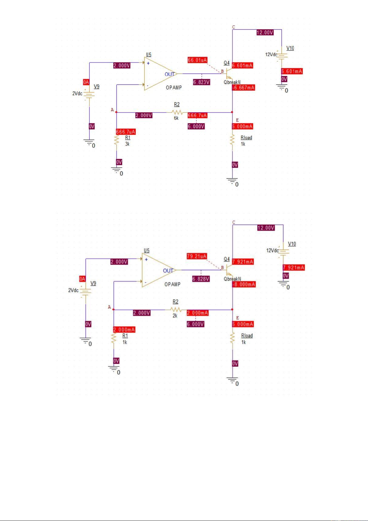
Students are proposed to implement this circuit on PSPICE with input is 2V and
the gain is 3. The voltage supply for the load side is 12VDC. Value of RLOAD is 1K.
Figure 1.5: Opamp follower with gain for the output
The simulation results in PSPICE (bias configuration) are presented here.
Moreover, a short explanations are required in this report to explain the gain of the output follower voltage.
We have the gain is 3. So 3=1+2 1 2 =>1 =2 =>2 =2×1
In order to verify that =3× , we can choose 2 different values for R2 and R1 lOMoARcPSD| 36991220
The bias point simulation when R2 = 6(kΩ) and R1 = 3(kΩ)
The bias point simulation when R2 = 2(kΩ) and R1 = 1(kΩ) For the
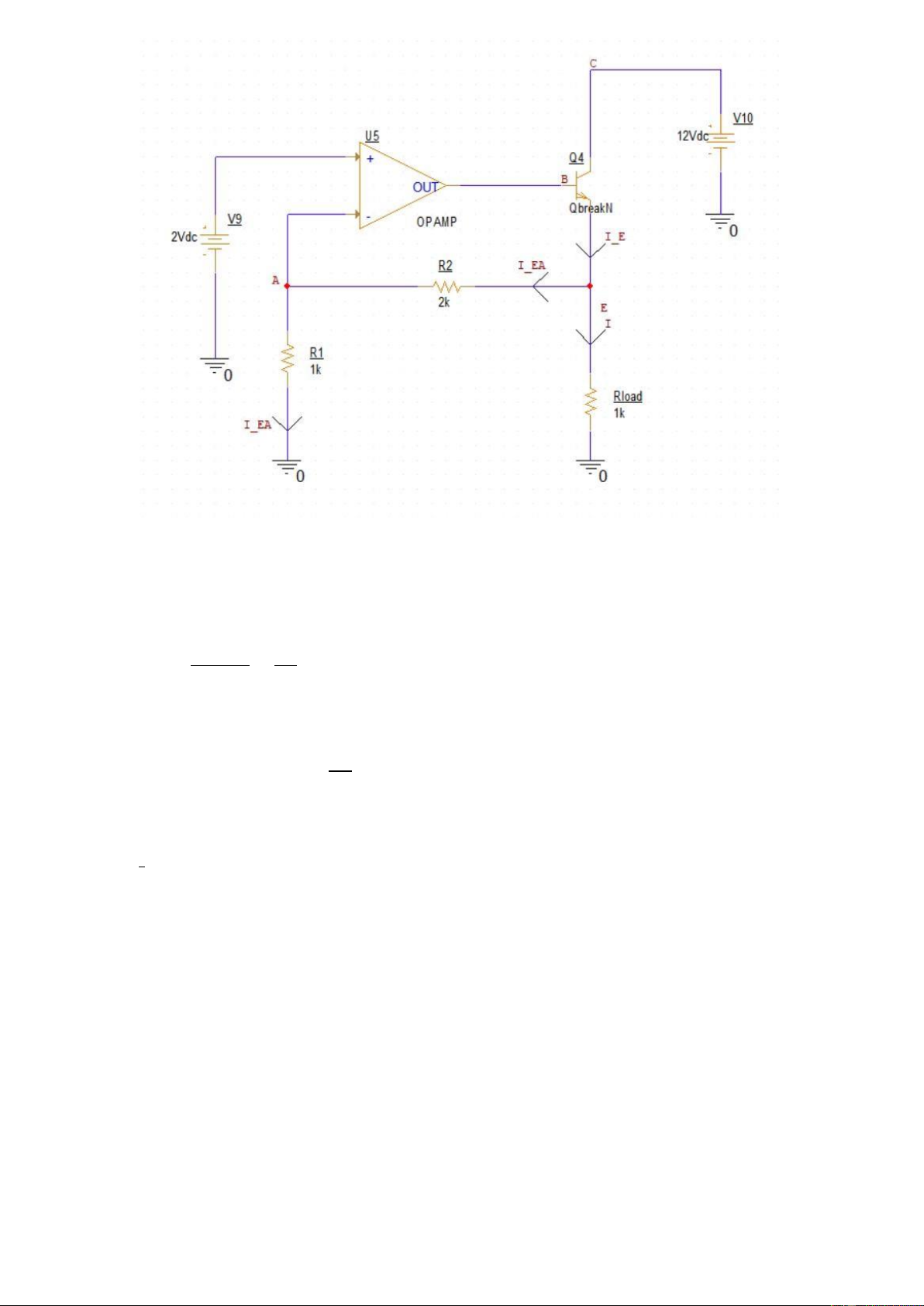
theoretical calculation, we can define the direction of the current as
shown in the following diagram: lOMoARcPSD| 36991220 The flow of the current
The Op-amp has negative feedback so =(+) =2() =−1 0=21 2 − = ×2 => =+×2 =2+ 1×21 =6()
It is obvious that as long as the values of R2 and R1 still follow the relation
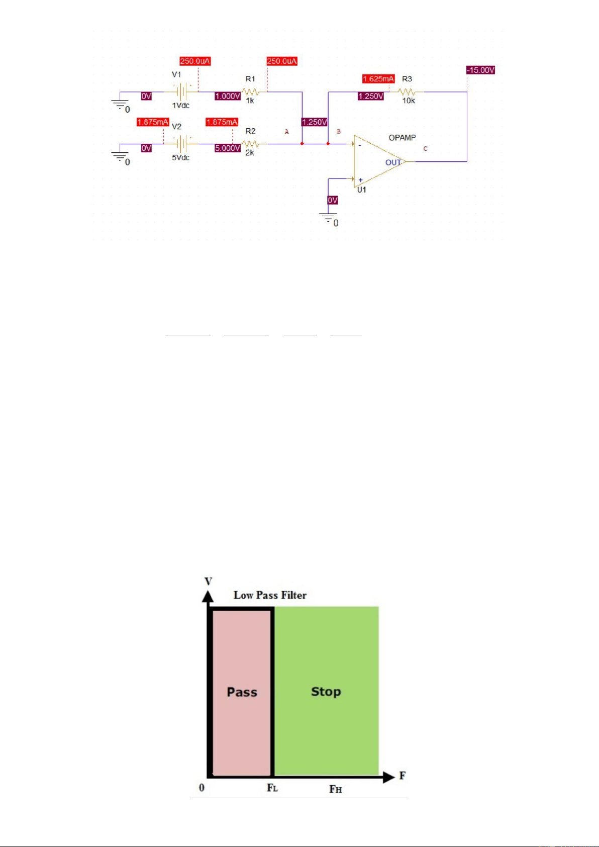
21 =2 , we always have =3×=6() 3.4 Summing Amplifier
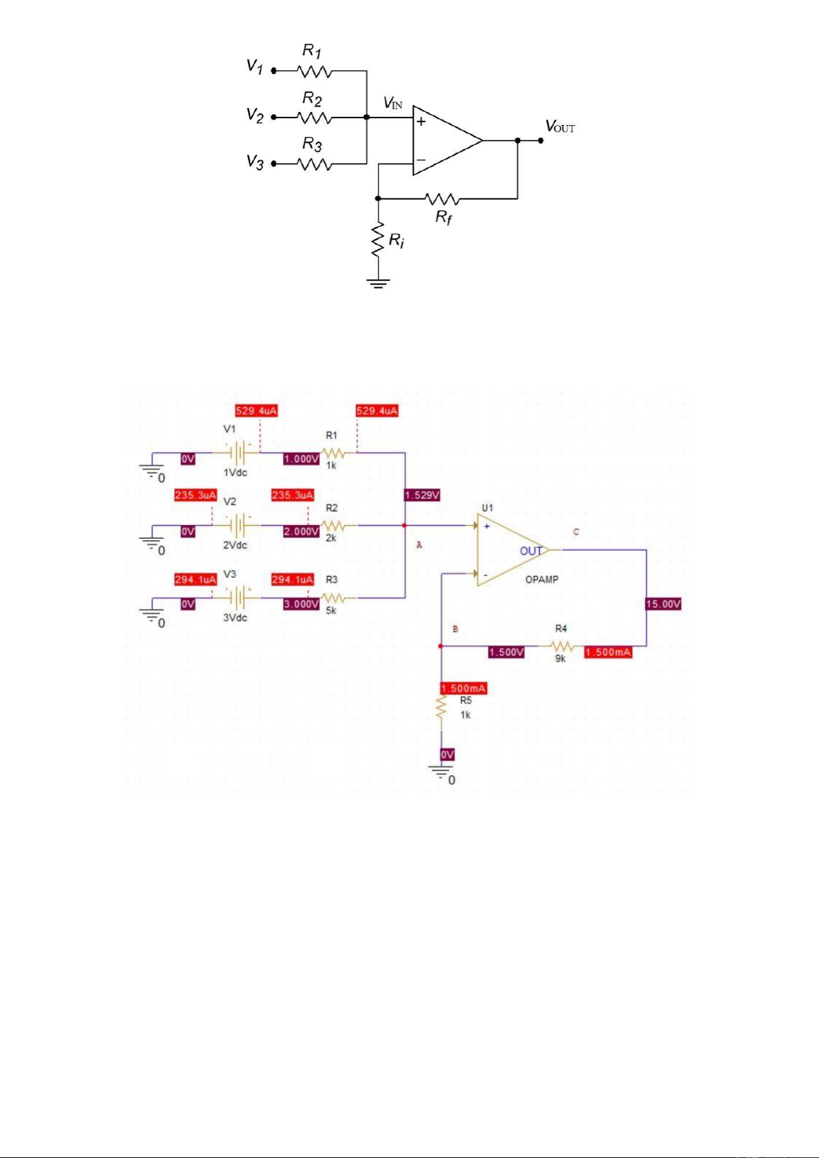
Students are proposed to implement following schematic in PSPICE and run the
simulation with R1 = 1K, R2 = 2K, R3 = 5K, Rf = 9K, Ri = 1K. There inputs are
V1 = 1V, V2 = 2V and V3 = 3V. This circuit is a non inverting summing configuration using opamp. lOMoARcPSD| 36991220
Figure 1.6: Non inverse summing using OPAMP
Students are proposed to design the schematic and place the results in this report.
Your image goes here The bias point simulation
Your calculations go here to explain the value of VOUT
Let I1, I2 and I3 denote the current through R1, R2 and R3, respectively. And
assume that the direction of these current are from A to their sources. We have
the following system of 4 equations with 4 unknowns: −1 =10001 −2 =20002 −3 =50003 1+2+3 =0
The last equation is the property of the Op-amp when it has negative feedback, I(+) = 0(A) lOMoARcPSD| 36991220 −1=10001 −2=20001 −3=50001 1+2+3 =0 => 1 =529.41() 2 =−253.58() 3 =−294.11() =1.529()
The negative values of I2 and I3 simply indicate that their directions are from the source to A.
Because of the negative feedback, VB = VA = 1.529(V ) =−0=1.529−0=1. 529() 1000
=+× =1.529+1.529×10−3×9000=15.29()
This value is matched with the simulation.
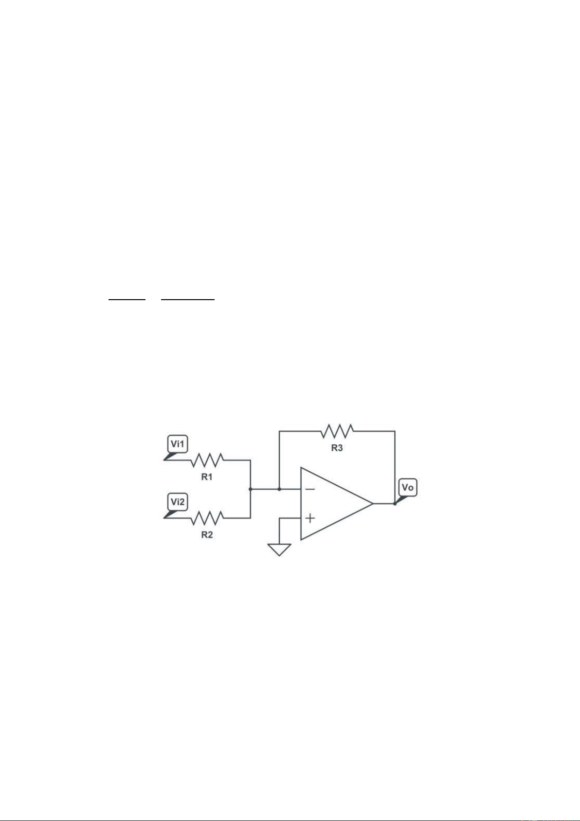
The second type of the summing amplifier is proposed as follows:
Figure 1.7: Inverse summing using OPAMP
Students are proposed to do the same steps above, with R1 = 1K, R2 = 2K, R3 = 10K and V1 = 1V, V2 = 5V. lOMoARcPSD| 36991220 The bias point simulation
Because of negative feedback of the Op-amp, we have VA = VB = V(+) = 0(V )
= 1+2 =1−1+2−2 =110−000+520−000=3.5()
=+×3 =0−3.5×10−3×10000=−35()
This results is different from what we have seen in the simulation since the
simulation did not consider the values of VA and VB as 0 V like the theoretical aspect. 3.5 Low Pass Filter
Low pass filter is a filter which passes all frequencies from 0Hz (DC current) to
upper cutoff frequency fH and rejects any signals above this frequency. A picture
to demonstrate a low pass filter behavior is shown in the figure bellow: lOMoARcPSD| 36991220
Figure 1.8: Low pass filter principles
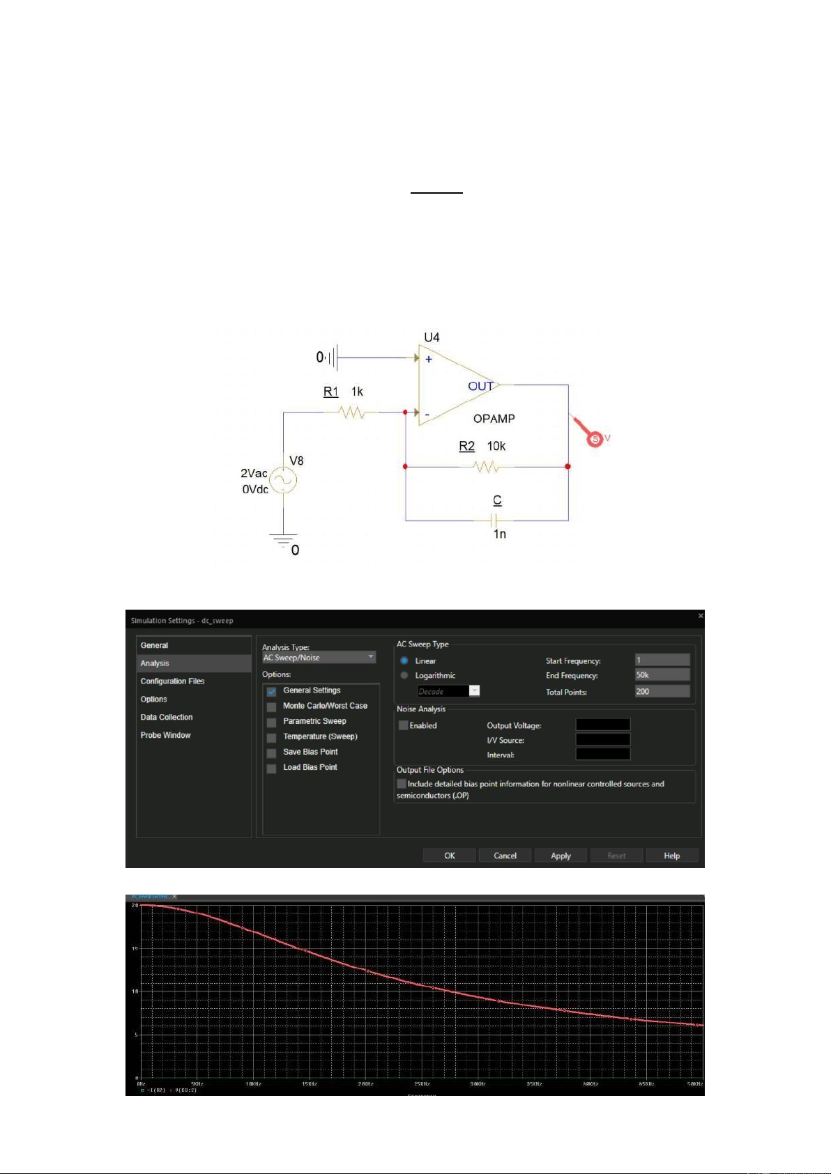
Similar to the closed loop configuration, there also 2 types of low pass filter,
including the inverting and non-inverting low pass filter. The figure bellow is an
inverting low pass filter. The cut-off frequency is determined by this equation: 1 =22
By applying the value of R2 = 10KOhm and C = 1nF, the cut-off frequency is
around 16K Hz. In order to see the results, students are proposed to run the AC
Sweep simulation profile (Linear Type, Start and Stop frequency are 1Hz
and 50kHz, 200 points), as follows:
Figure 1.9: Inverting low pass filter
Figure 1.10: AC Sweep simulation profile lOMoARcPSD| 36991220
Figure 1.11: Simulation results
The final results can be archived like the figure bellow:
It is said that the cut-off frequency point having the gain reduced 3dB. The
gain at 0Hz is 10 (input voltage is 2V and output voltage is 20V), or 20log (10)
= 20dB, meanwhile, the gain at 16kHz is 7 (input voltage is 2V and output
voltage is 14V), or 20log (7) = 16.9.
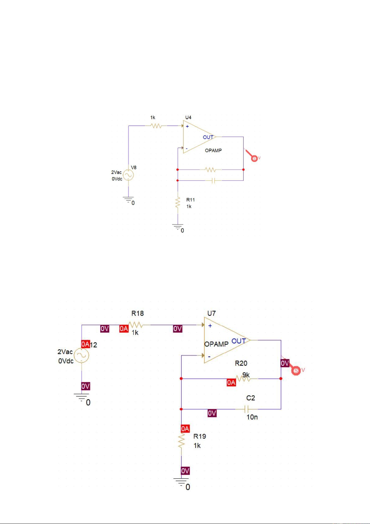
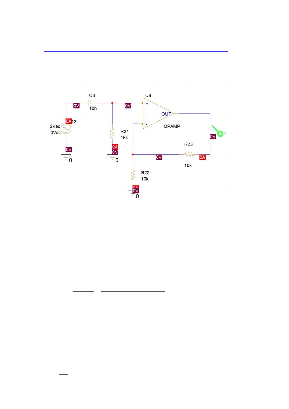
The second type of a low pass filter, the non-inverting configuration, is presented as follows
Figure 1.12: Non-inverting low pass filter
Students are proposed to calculate the value of R and C to have the amplifier
factor equal to 10 and the cut-off frequency is the same as the previous
example. The simulation result with AC Sweep mode is required to plot in this report as well. lOMoARcPSD| 36991220
The voltage gain of a non-inverting operational amplifier is given as: 20 =1+ 19 20 => 10=1+ 2000 => 20 =9(kΩ)
The cut-off frequency is given as being 16 kHz with an input impedance R18 of
1kΩ. This cut-off frequency can be found by using the formula: 1 = 2182 1 1
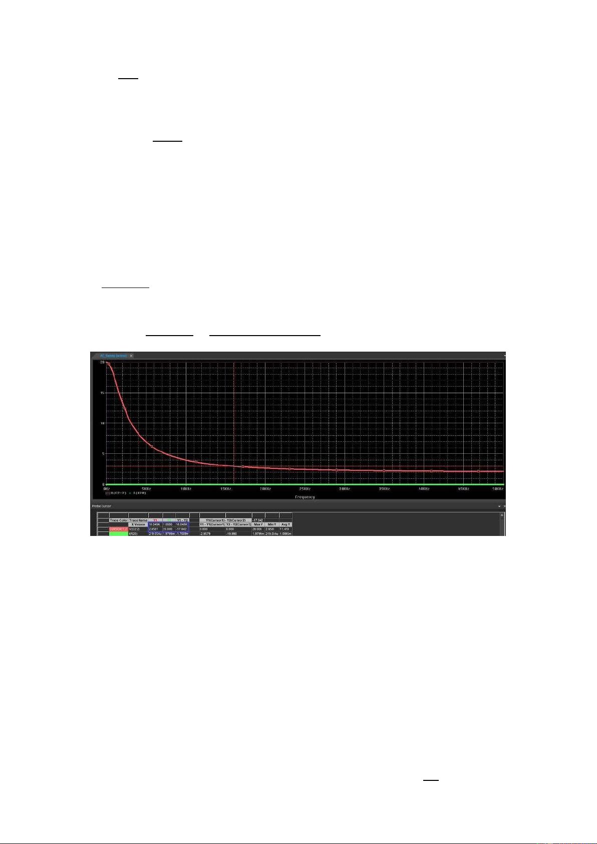
=> 2 =218 =2×16000×1000=10() The AC Sweep result
For this circuit the cut-off frequency point having the gain reduced nearly 16.6
dB. The gain at 0 Hz is 10 (input voltage is 2V and output voltage is 20V) or
20×log () = 20(dB), meanwhile, the gain at 16 kHZ is 3.4 dB (input voltage
is 2V and output voltage is 2.9581V)or 20×log () = 3.4dB
Here due to the position of the capacitor in parallel with the feedback resistor
R20, the low pass frequency is set as before but at high frequencies the reactant
of the capacitor dominates shorting out R20 reducing the amplifiers gain.
At a high enough frequency the gain bottoms out at unity (0 dB) as the amplifier
effectively becomes a voltage follower so the gain equation 1 + 0 19 which equals 1 (unity) lOMoARcPSD| 36991220 3.6 High Pass Filter
In contrast to the low pass filter, there is a high pass filter, which can be referred from this link:
https://www.allaboutcircuits.com/video-tutorials/op-amps-low-pass-and- highpass-active-filters/
Students are proposed to implement a high pass filter in PSPICE and explain the
behaviors of your high pass filter
Active high pass filter with amplification.
The pass band gain of this non-inverting operational amplifier is Af = 2
The cut-off frequency is fc = 1(kHz) The capacitance C3 is 10 (nF).
We have the formula of the cut-off frequency is: 1 =2213 1 1
=> 21 =23 =2×10×10−9×1000=15.92(Ω)
Or 16 Ω to the nearest preferred value
The pass band gain of the filter, Af is 2. 23 =1+ 22 23 => =1 22 lOMoARcPSD| 36991220
We can therefor select a suitable value for the two resistors of say, 10 kΩ each for both feedback resistors. The AC sweep result
This first-order high pass filter,consists simply of one op-amp, one capacitors
and three resistors. The amplitude of the signal in increased by the gain of the amplifier.
It only allows the frequencies that are higher than the cut-off frequency to pass
through and all of those which are lower than fC will be filtered out.
Low frequencies are then shorted to ground through R3, and high frequencies are
passe to the input of the op-amp. In both case, the op-amp produces a buffered version of the output.
3.7 Comparator with Hysteresis (Schmitt Trigger)
The two resistors R1 and R2 act only as a "pure" attenuator (voltage divider).
The input loop acts as a simple series voltage summer that adds a part of the
output voltage in series to the circuit input voltage. This series positive feedback
creates the needed hysteresis that is controlled by the proportion between the
resistances of R1 and the whole resistance (R1 and R2). The effective voltage
applied to the op-amp input is floating so the op-amp must have a differential input. lOMoARcPSD| 36991220
Figure 1.13: Inverting Schmitt trigger
The circuit is named inverting since the output voltage always has an opposite
sign to the input voltage when it is out of the hysteresis cycle (when the input
voltage is above the high threshold or below the low threshold). However, if the
input voltage is within the hysteresis cycle (between the high and low
thresholds), the circuit can be inverting as well as non-inverting. The output
voltage is undefined and it depends on the last state so the circuit behaves like an elementary latch.
In PSPice, this trigger is implemented as follows, with 3 voltage markers:
Figure 1.14: Schmitt trigger in PSPICE
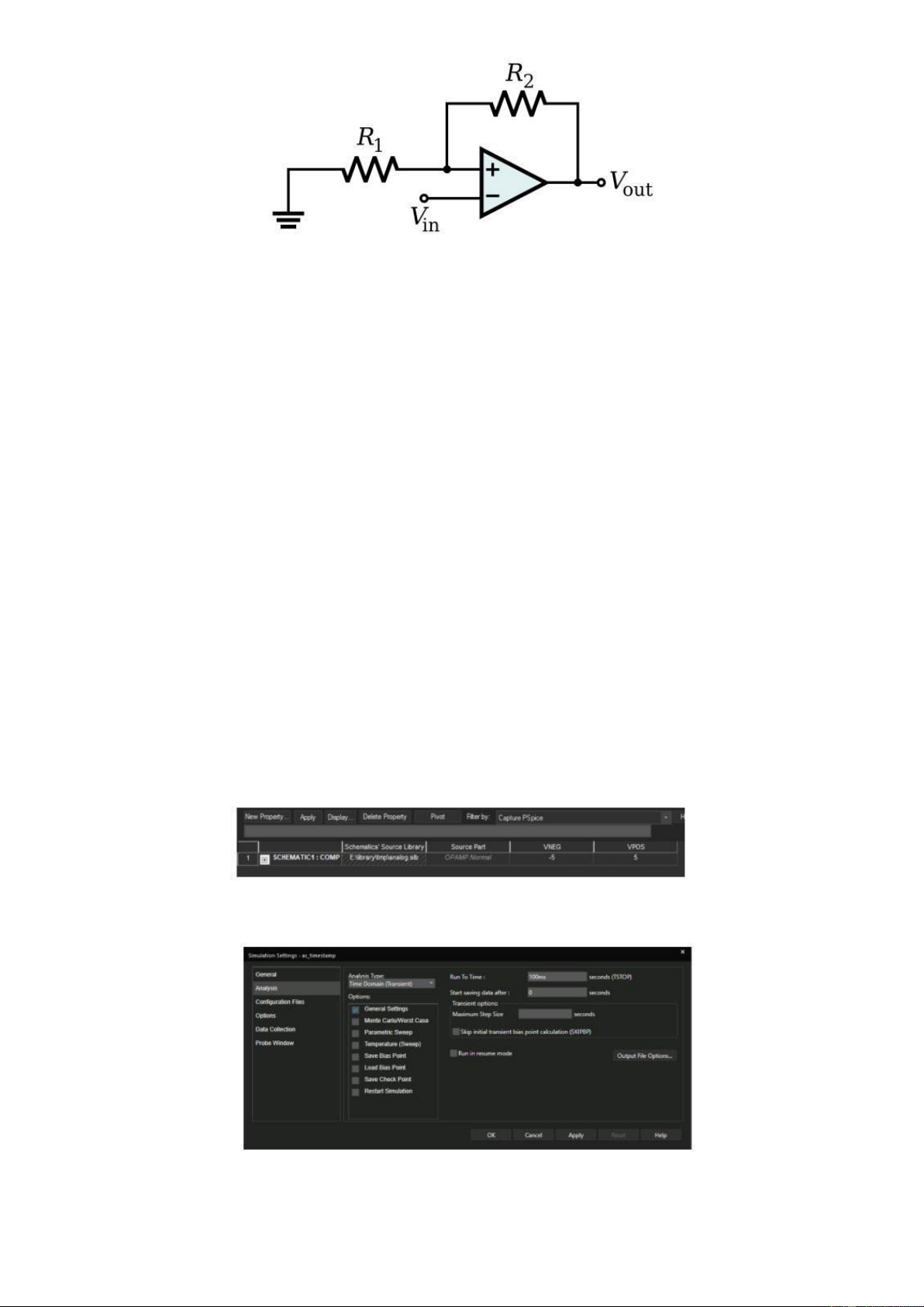
The OPAMP device is modified in the Properties windows (right click on the
component and chose Edit Properties or double click on the component), in order
to set the VPOS and VNEG to +5V and -5V, as follows:
The simulation profile in this exercise is the Time Domain, and is configured as follows:
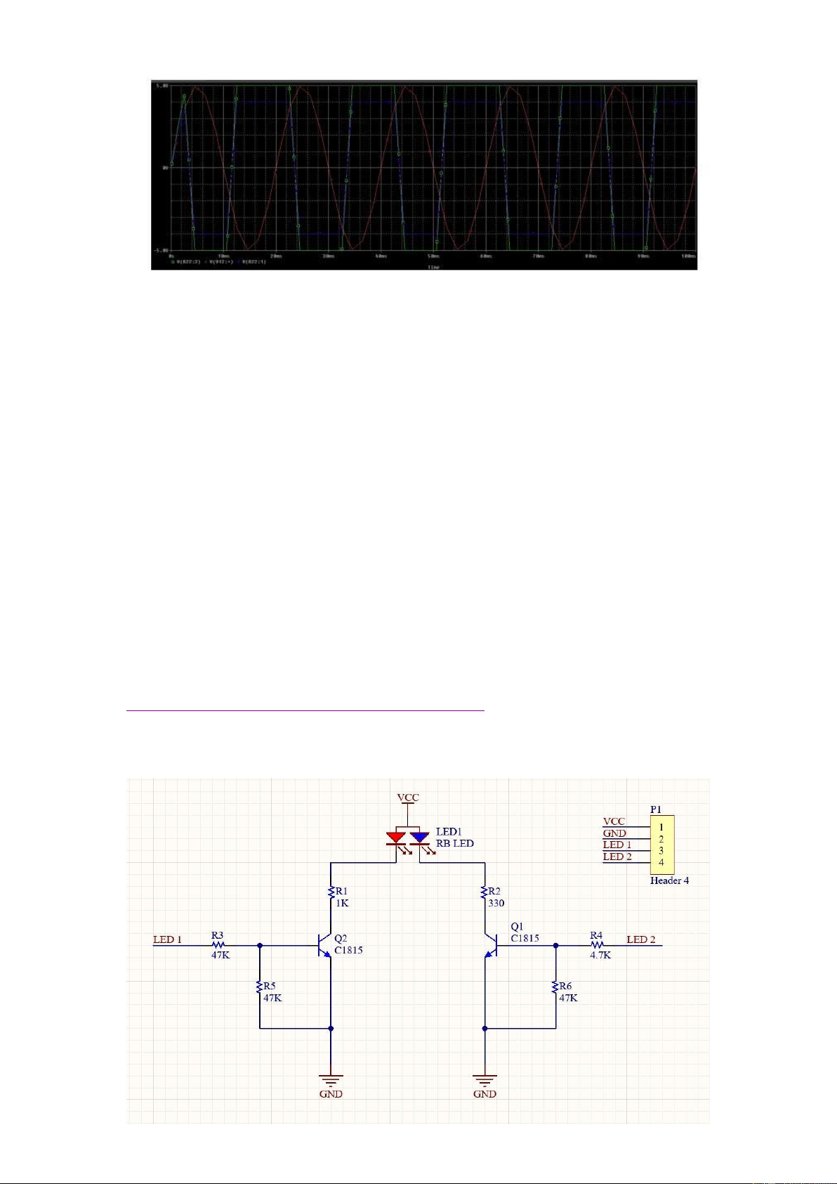
Finally, the simulation results can be archived as follows:
Students are proposed to explain the signal at the output of the opamp. Why
the signal is toggled at +4V and -4V
Figure 1.15: Schmitt trigger in PSPICE lOMoARcPSD| 36991220
Figure 1.16: Simulation profile
Figure 1.17: Schmitt trigger simulation results
The signal is toggled at +4V and -4V because the input loop act as a simple series
voltage summer that adds a part of the output voltage in series to the circuit input voltage.
This series positive feed back creates the needed hysteresis that is controlled by
the proportion between the resistances of R1 and the whole resistance. 4 Altium Designer 4.1 LED Driver
In this project, we will show how to build a simple LED driver circuit. A simple
driver based on BJT is proposed in this section. 4.1.1 Schematic design The manual for the schematic is posted in this link:
https://www.youtube.com/watch?v=ftiX8peTsiw
Students are proposed to design the schematic and place the results in this report.
Your image goes here lOMoARcPSD| 36991220
The schematic design of the LED Driver 4.1.2 PCB layout The manual for PCB layout is posted in this link:
https://www.youtube.com/watch?v=btpAoh3nmBU
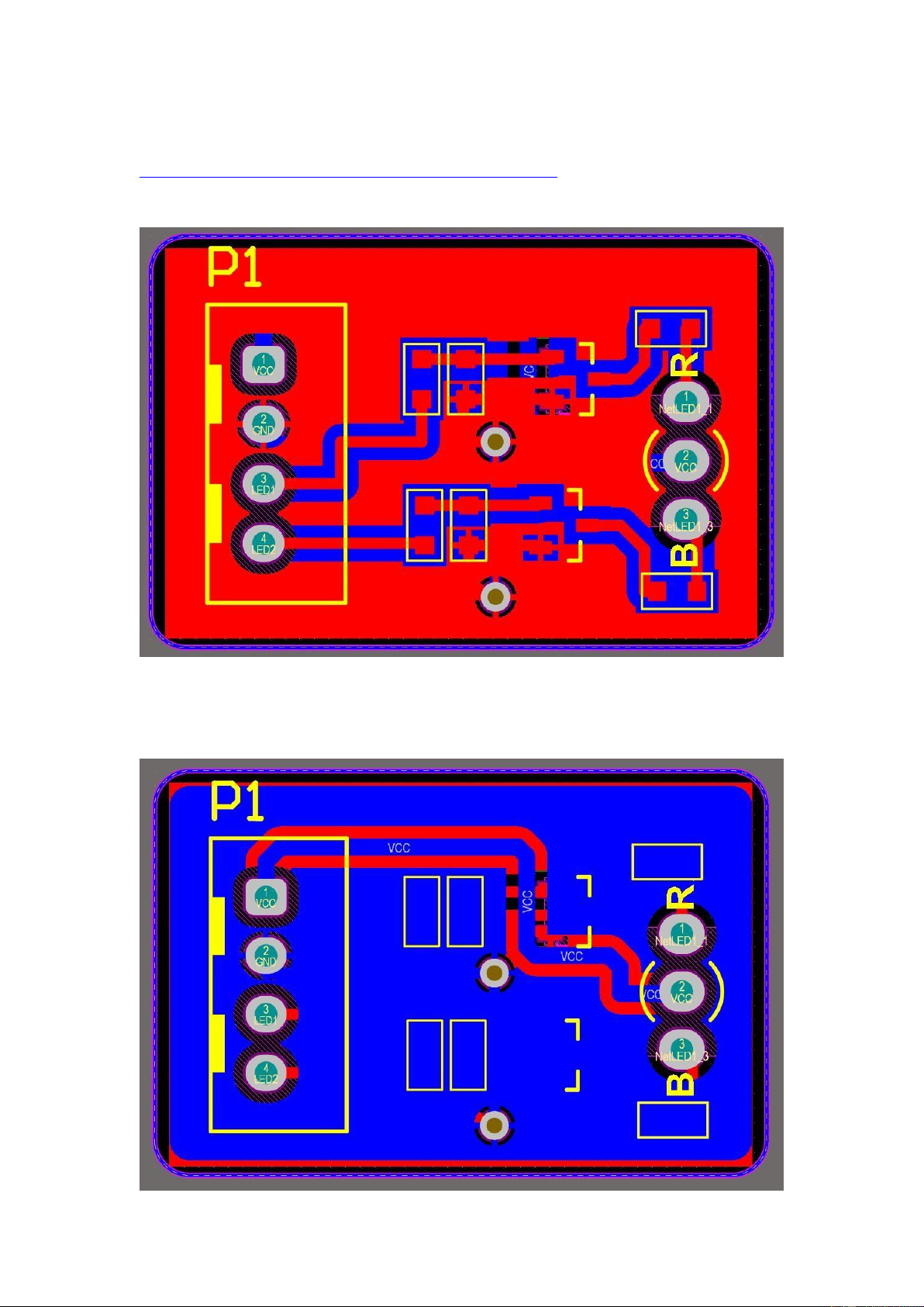
Your image goes here
The top layer of the PCB layout
The bottom layer of the PCB layout lOMoARcPSD| 36991220
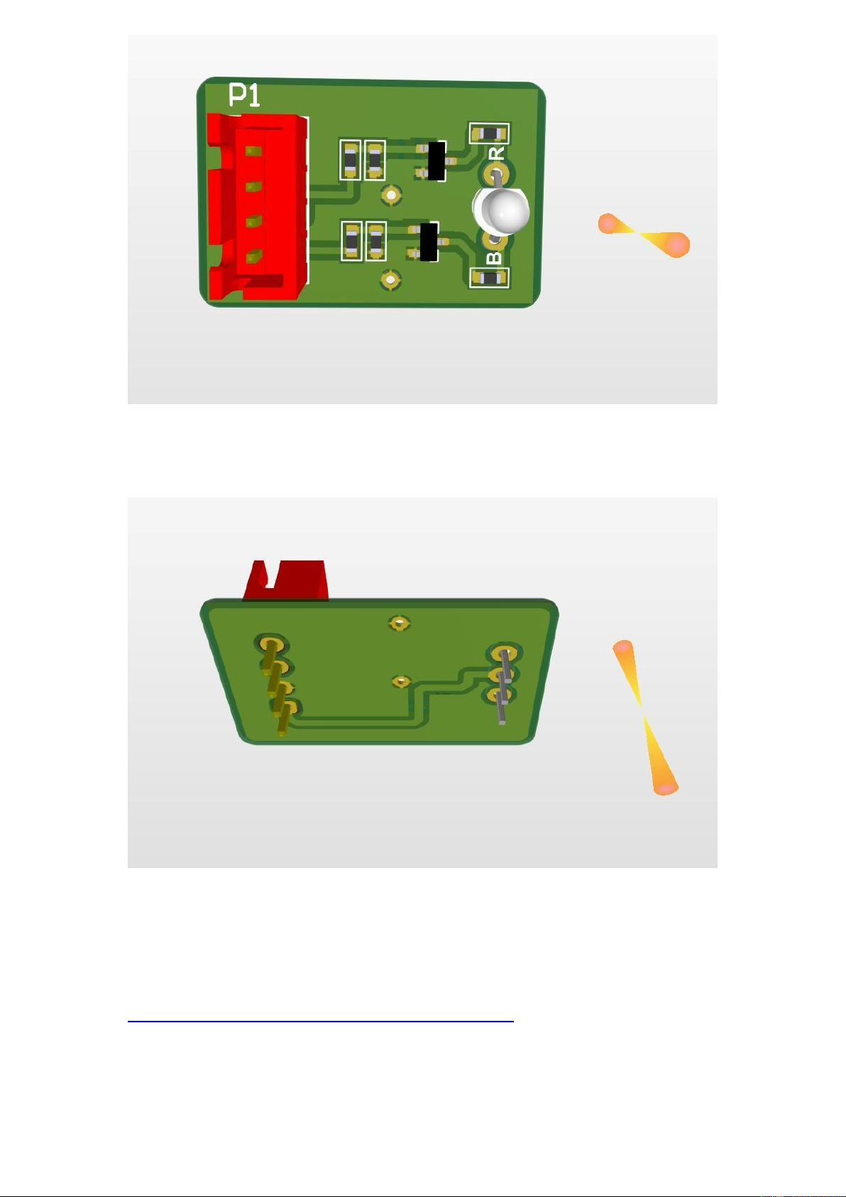
The top view of the LED Driver in 3D
The bottom view of the LED Driver in 3D 4.2 Relay Controller 4.2.1 Schematic design The manual for the schematic is posted in this link:
https://www.youtube.com/watch?v=VcO_F97ydFM
Students are proposed to design the schematic and place the results in this report. lOMoARcPSD| 36991220
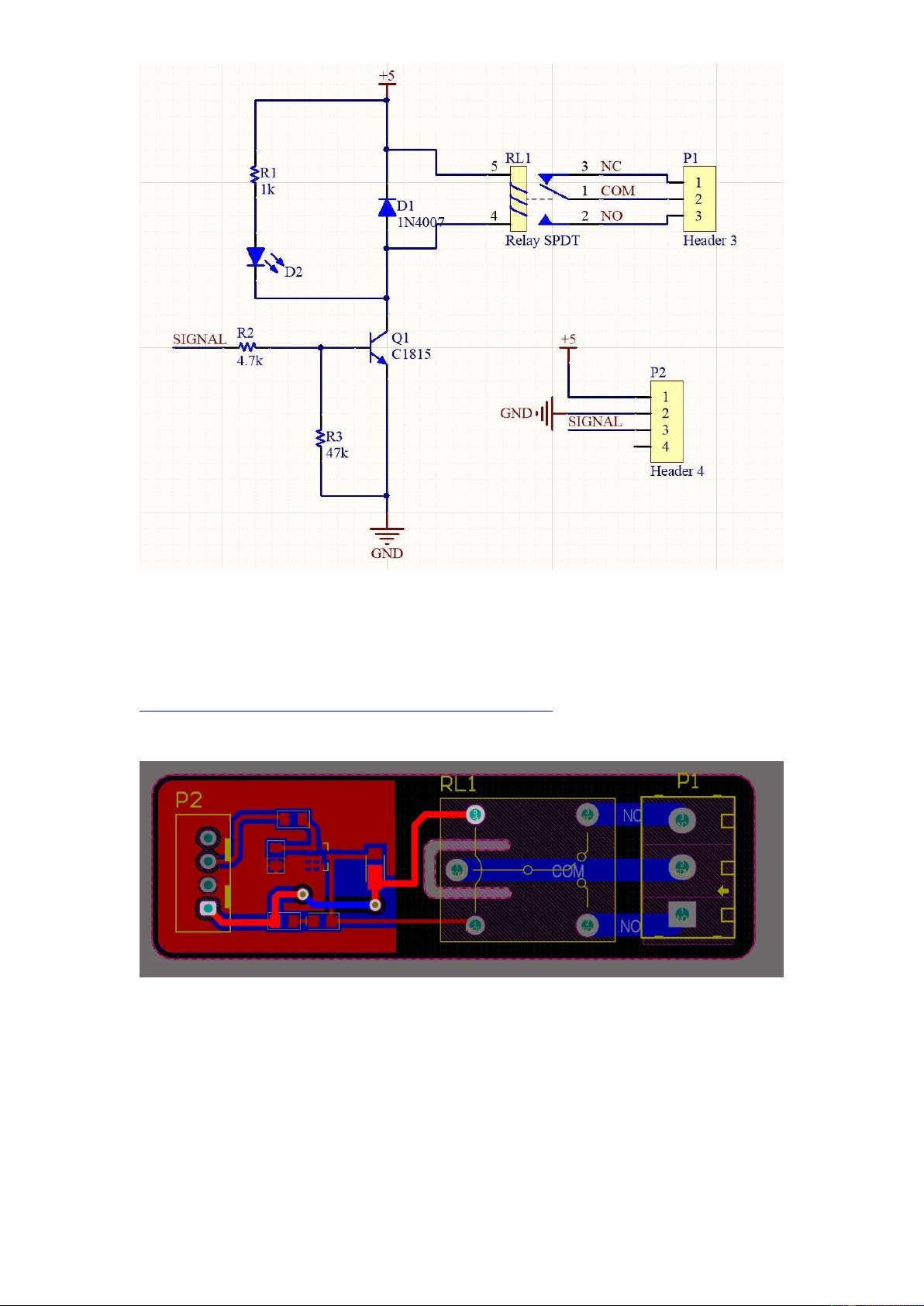
Your image goes here
The schematic design of the Relay Controller 4.2.2 PCB layout The manual for PCB layout is posted in this link:
https://www.youtube.com/watch?v=Dbqcb0zQ0E8
Your image goes here lOMoARcPSD| 36991220
The top layer of the PCB layout
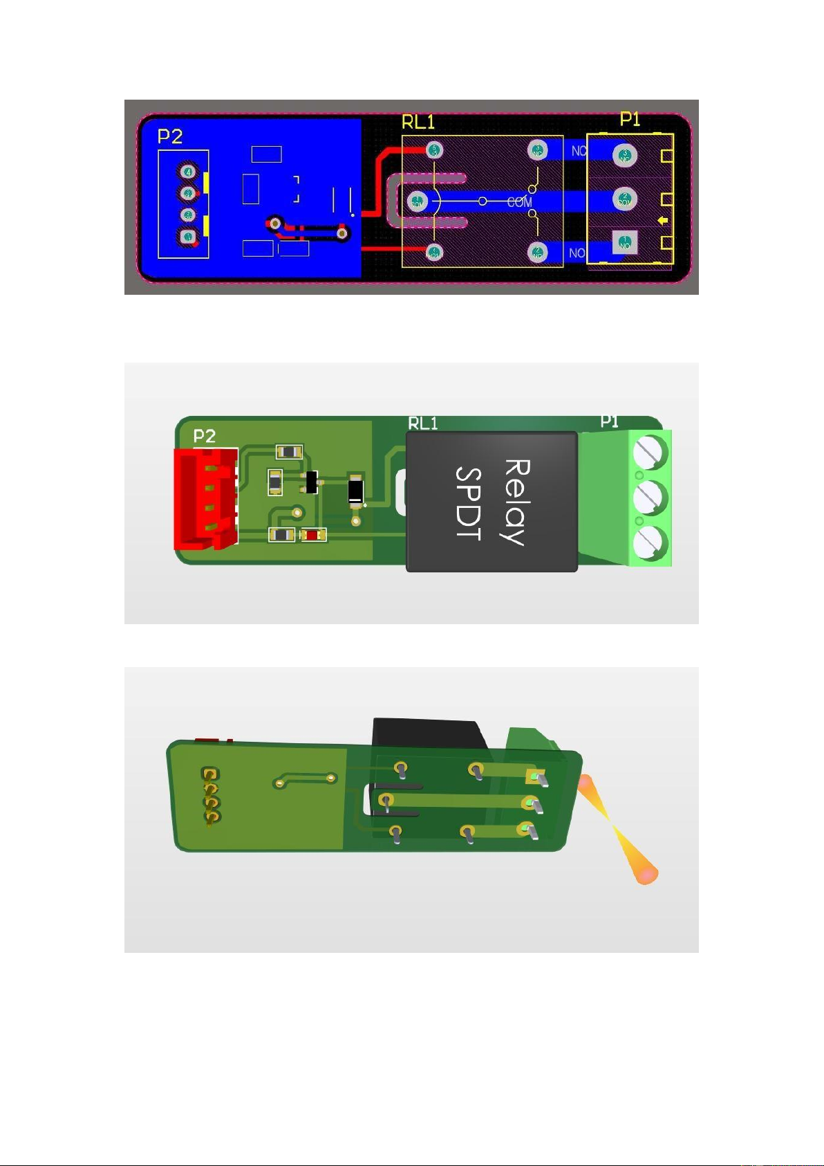
The bottom layer of the PCB layout
The top view of the Relay Controller in 3D
The bottom view of the Relay Controller in 3D