công nghệ bán dẫn Chapter 3_Bipolar Junction Transistors


Preview text:
Faculty of Electrical and Electronic Engineering
Semiconductor Technology Dr. Le Viet Thong
Email: thong.leviet@phenikaa-uni.edu.vn phenikaa-uni.edu.vn
Chapter III: Bipolar Junction Transistors Contents:
III.1. Bipolar Junction Transistor (BJT) Structure III.2. Basic BJT Operation
III.3. BJT Characteristics and Parameters III.4. Voltage-Divider Bias III.5. Other Bias Methods III.6. The BJT as an Amplifier III.7. The BJT as a Switch III.8. The Phototransistor III.9. Troubleshooting phenikaa-uni.edu.vn Goals
• Understand BJT structure and its basic operation
• Explore the differences between NPN and PNP transistors
• Study important BJT parameters and characteristic curves
• Analyze simple transistor circuits
• Understand bias methods to analyze the BJT circuit
• Define the operation point (Q-point) of BJT circuit
• Explore the applications of BJT as switch and amplifier phenikaa-uni.edu.vn New words
BJT Bipolar Junction transistor (transistor lưỡng cực)
Emitter Cực phát
Collector Cực thu
Base Cực nền
Current gain Hệ số khuếch đại dòng điện (DC)
Load line Đường tải
Q-point Điểm Q, điểm hoạt động (quiescent point)
Saturation Bão hòa
Amplification Khuếch đại phenikaa-uni.edu.vn Remarks phenikaa-uni.edu.vn
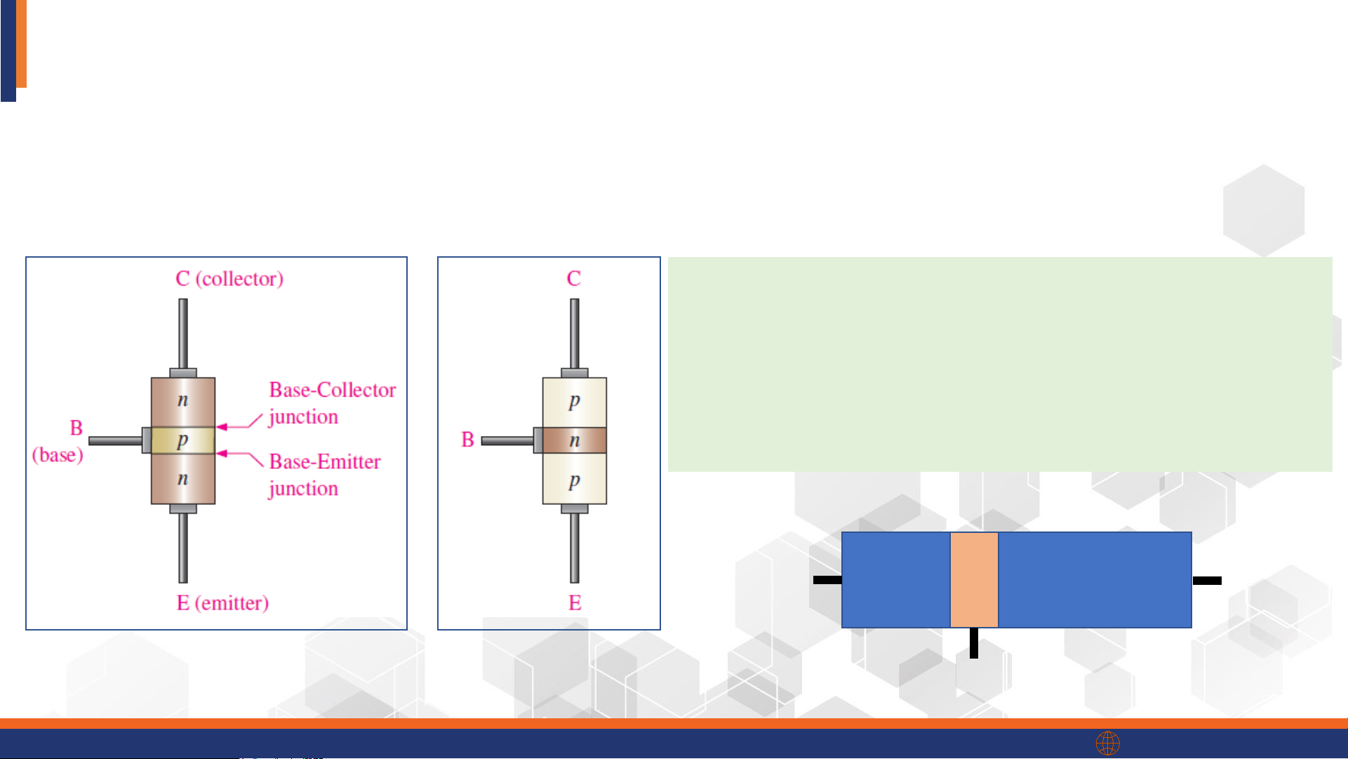
III.1. Bipolar Junction Transistor Structure
• Bipolar Junction Transistor (BJT) is constructed with three doped
semiconductor regions separated by two PN junctions.
• Three regions: Emitter (E), Base (B), and Collector (C)
❖ The Base region is lightly doped NPN PNP
semiconductor, and very thin.
❖ The Collector is the largest and
moderately doped region.
❖ The Emitter is the heavily doped region. E n++ p n+ C B phenikaa-uni.edu.vn
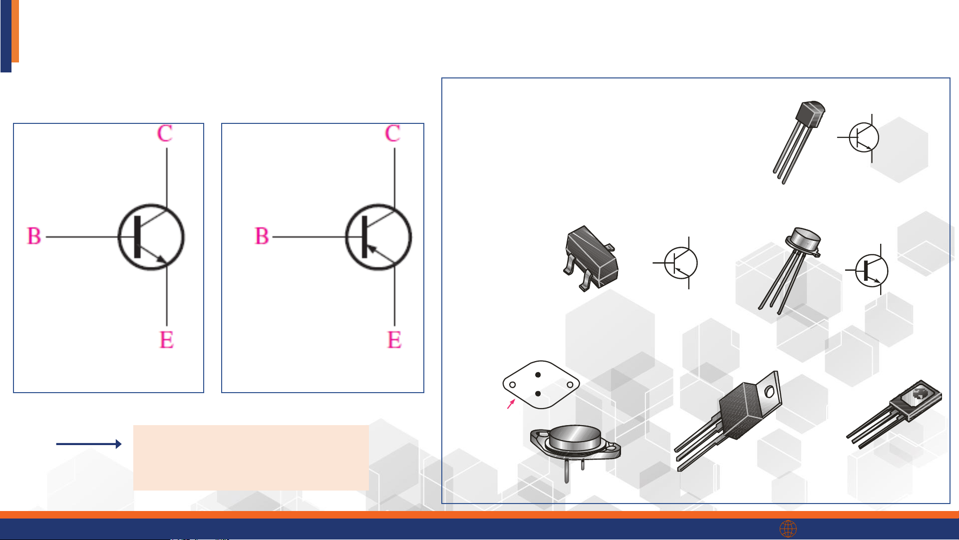
III.1. Bipolar Junction Transistor Structure Symbols
Common Transistor Packages 3 Collector 2 Base 1 1 Emitter 2 3 TO-92 3 Collector 3 3 Collector 1 2 1 Base Base 2 2 Emitter 1 Emitter 3 2 SOT-23 1 TO-18 E NPN PNP B C C (case) E Arow show the B C C B E direction from P to N TO-3 TO-220AB TO-225AA phenikaa-uni.edu.vn
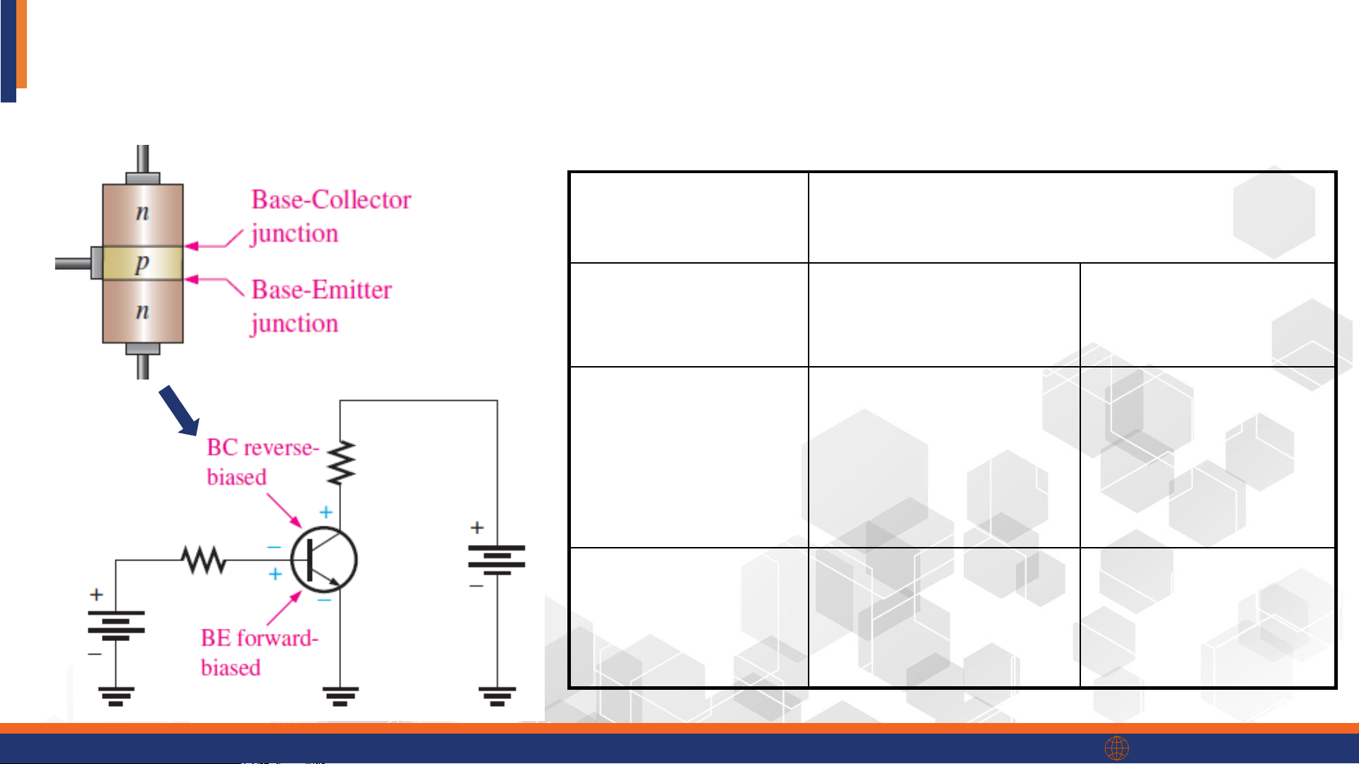
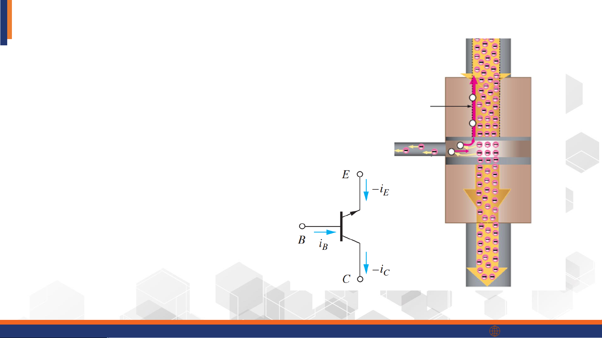
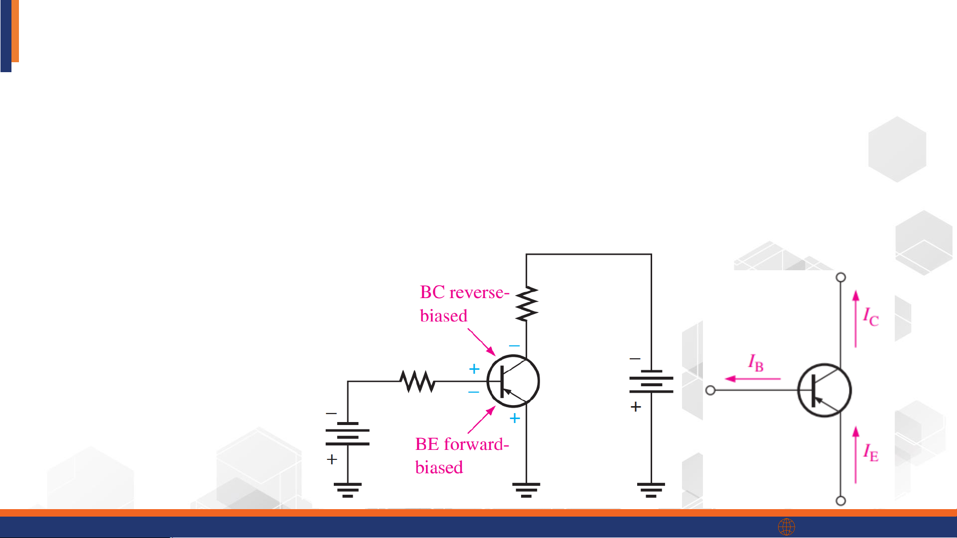
III.2. Basic BJT Operation NPN transistor
Operation regions of bipolar transistors C Base-Emitter Base-Collector Junction Junction B Reverse Bias Forward Bias E Forward-Active Saturation Region Region Biasing Forward Bias (Good (Closed Amplifier) Switch) Reverse-Active Cutoff Region Reverse Bias Region (Open Switch) (Poor Amplifier) phenikaa-uni.edu.vn III.2. Basic BJT Operation NPN transistor Forward-active
Base-Emitter (BE): forward biased (VBE > 0)
Base-Collector (BC): reverse biased (VBC < 0)
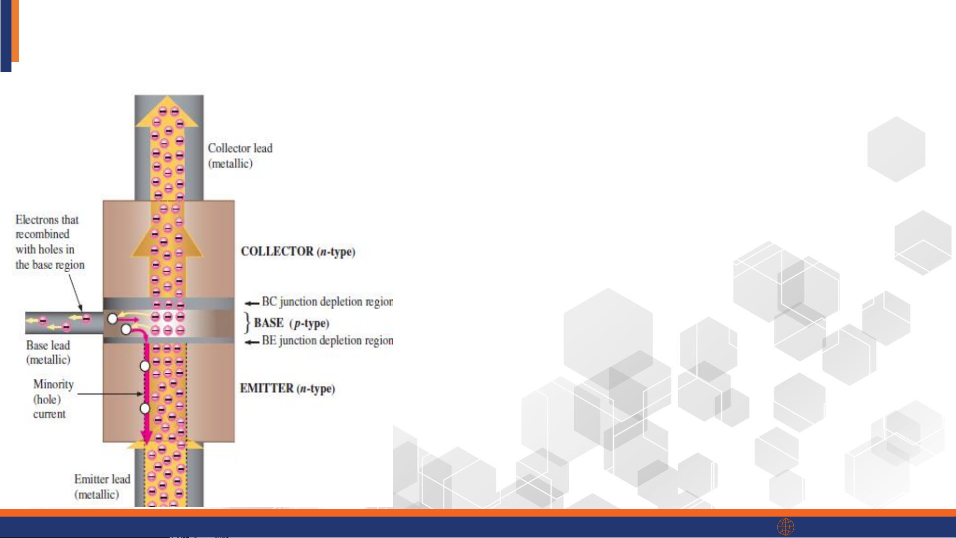
• Electrons diffuse from Emitter, cross the BE
junction, and enter Base (p-type).
• Holes injected from Base into Emitter
→ creating a minor hole current.
• Base is lightly doped, and very thin.
• In the Base, a small amount of electrons recombine with holes
→ producing the Base current.
• Most of free electrons reach the BC junction,
and are immediately swept into Collector due
to a strong electric field caused by reverse biased VBC. phenikaa-uni.edu.vn III.2. Basic BJT Operation NPN transistor Forward-active Electron flow Current flow
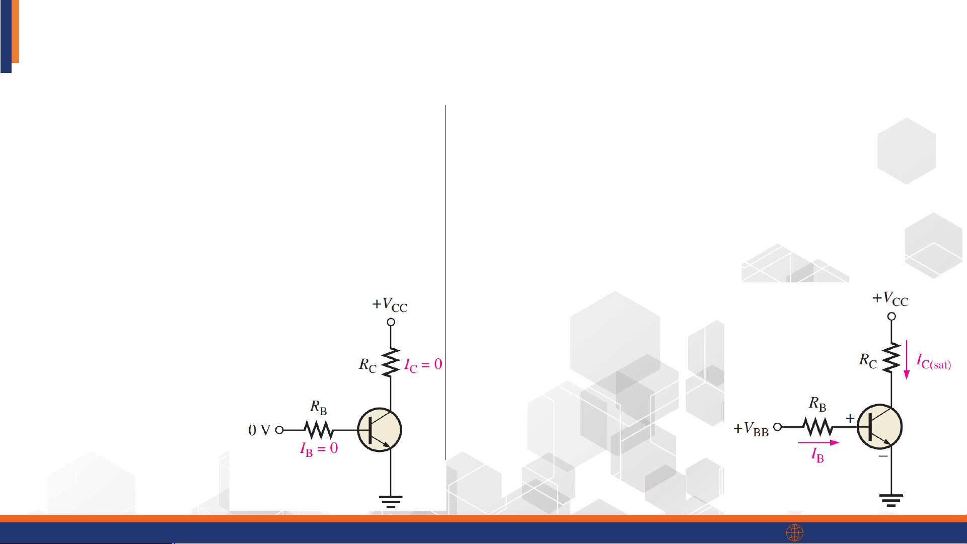
* The arrow on the emitter of the transistor symbols points in the direction of conventional current. phenikaa-uni.edu.vn III.2. Basic BJT Operation NPN transistor Cut-off Saturation BE reverse biased (VBE ≤ 0) BE forward biased (VBE> 0) BC reverse biased (VBC < 0) BC forward biased (VBC > 0)
• No current flow through the BJT. • VCE is small (~0.2 V) • IC=IE=IB= 0
• Electrons diffuse from Emitter into Base, but
• In fact, there is a very small
also from Collector into Base, leading to the reverse current ICEO which is
large increase in Base current IB. usually neglected (ICEO =0). • IC is independent on IB. BJT is OFF state BJT is ON state phenikaa-uni.edu.vn III.2. Basic BJT Operation NPN transistor Collector Reverse-active BE reverse biased (VBE < 0) BC forward biased (VBC > 0)
• Similar as the Forward-active mode, but the
current flow in reverse direction
• Due to the difference in doping Base
level of Emitter and Collector
regions, IC and IB in reverse-active
mode are smaller than that in forward-active mode Emitter phenikaa-uni.edu.vn Reverse-active
• Very low: βR≈ 1–10
• (vs. βF≈ 50–200 in forward active).
• Because the emitter is heavily
doped and the collector lightly doped → not optimized for reversed operation. phenikaa-uni.edu.vn III.2. Basic BJT Operation PNP transistor
• 4 operation mode as NPN transistor.
• Instead of electron, the major carrier is holes. The movement of hole from emitter to collector create the current.
• IC and IB exit transistor terminals and IE enters the device. Forward-active Mode phenikaa-uni.edu.vn
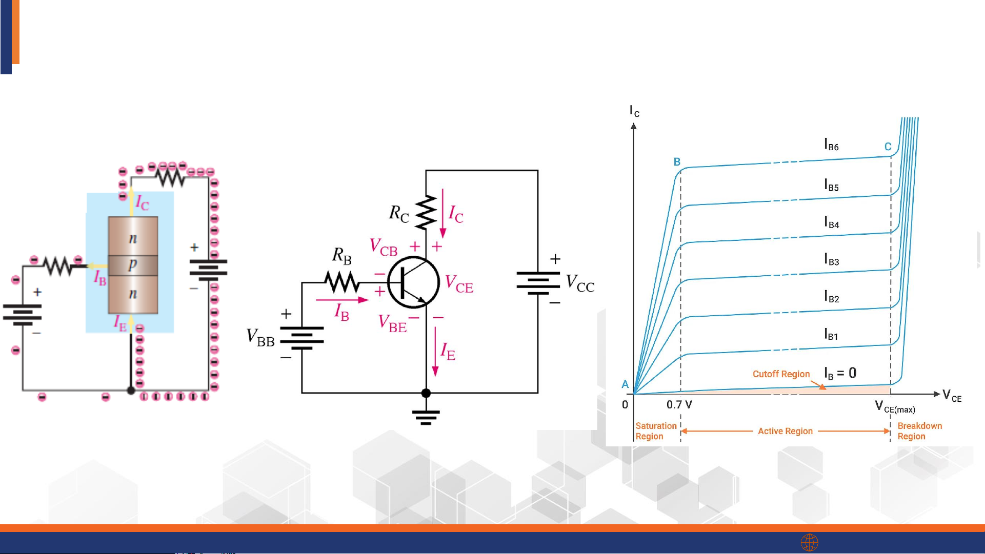
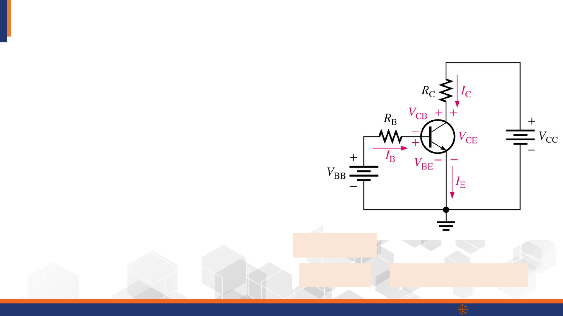
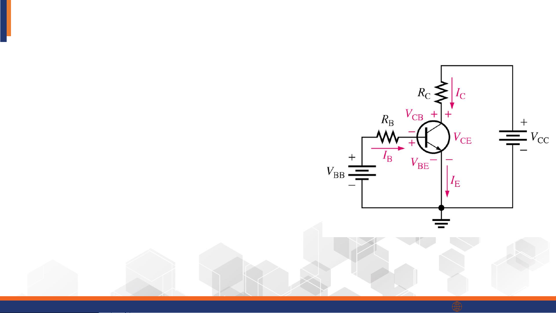
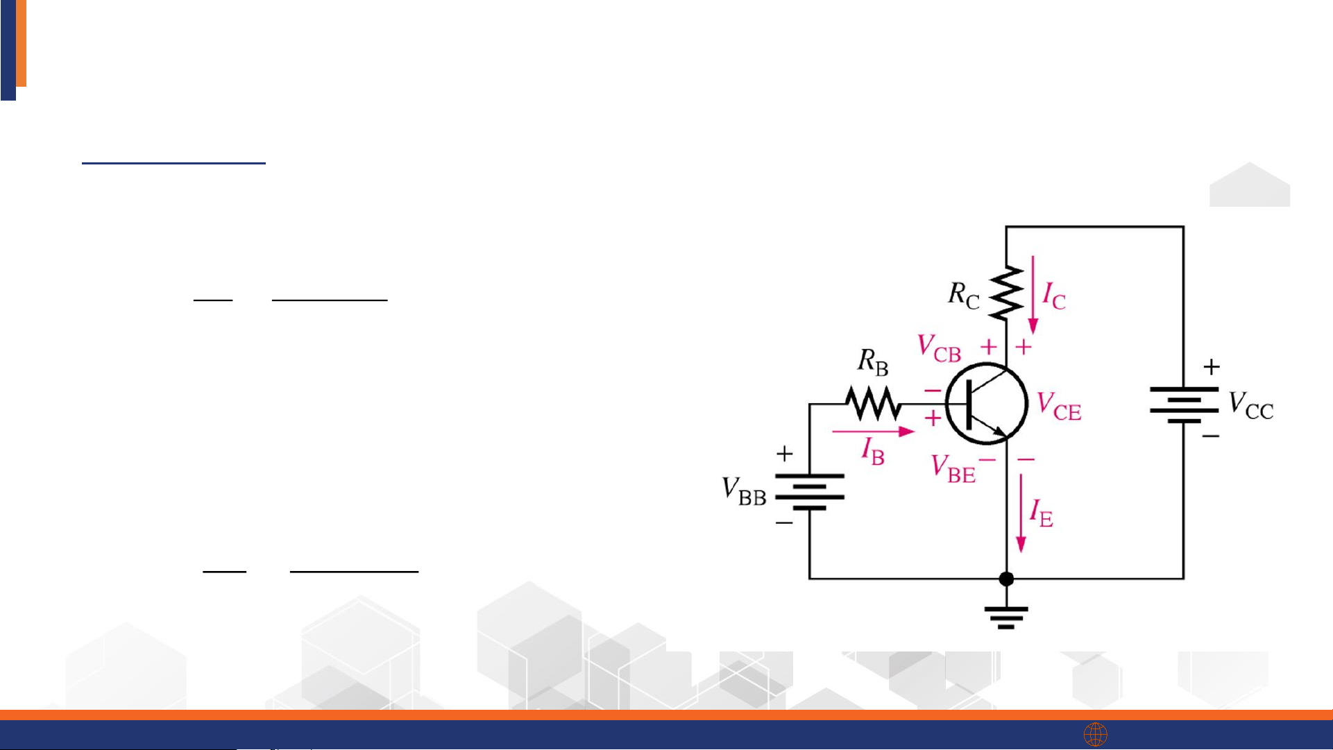
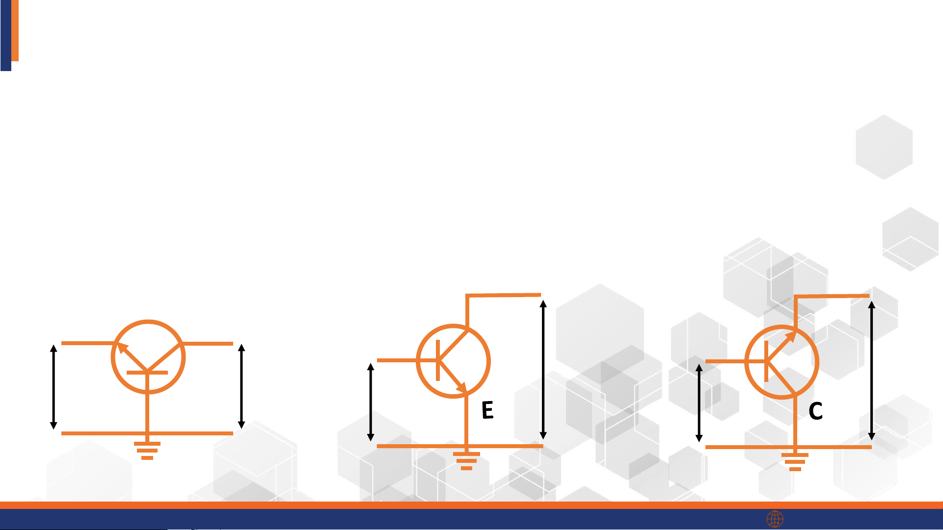
III.3. BJT Characteristics and Parameters NPN transistor
IB: base current
IE: emitter current
IC: collector current
VBE: voltage across base-emitter junction
(VBE ≅ 0.7 V)
VCB: voltage across collector-base junction
VCE: voltage from collector to emitter : current gain IE = IC + IB = IC/IB
α = IC/IE = /(+1) phenikaa-uni.edu.vn
III.3. BJT Characteristics and Parameters
Current and Voltage Analysis
When the base-emitter junction is forward-biased: VBE ≅ 0.7 V VR = I B BRB : by Ohm’s law
IBRB = VBB – VBE : substituting for VRB VCE = VCC – VRC VR = I C CRC VCE = VCC – ICRC
The voltage across the reverse-biased collector-base junction:
VCB = VCE – VBE where IC = β IB phenikaa-uni.edu.vn
III.3. BJT Characteristics and Parameters
Example 1: Determine βDC and IE for a transistor where IB = 50 μA and IC = 3.65 mA. I 65 . 3 = C = mA = 73 DC I 50 A B IE = IC + IB = 3.65 mA + 50 μA = 3.70 mA I 65 . 3 = C = mA = 98 . 0 6 DC I 70 . 3 mA E phenikaa-uni.edu.vn
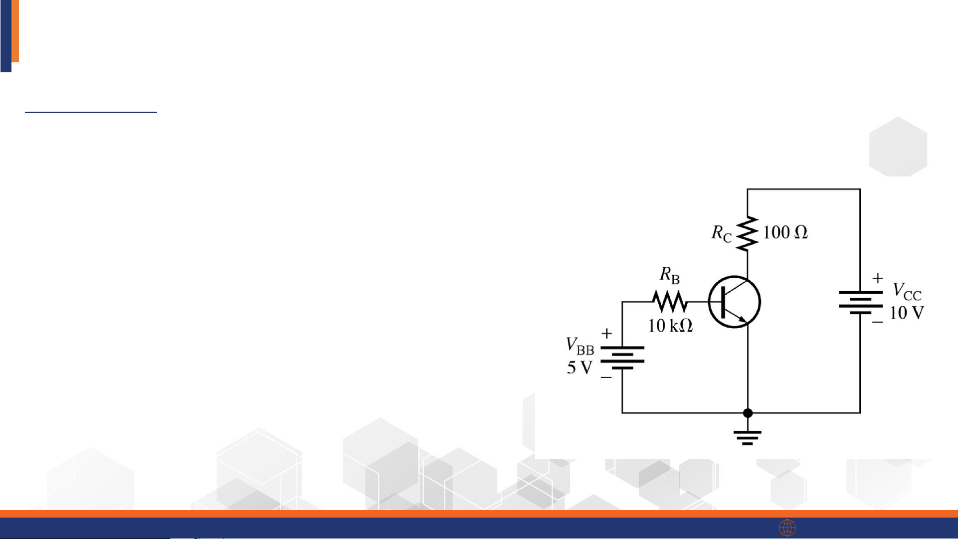
III.3. BJT Characteristics and Parameters
Example 2: Determine IB, IC, VBE, VCE, and VCB. Given: βDC = 150.
When the base-emitter junction is forward-biased, VBE ≅ 0.7 V
IB = (VBB – VBE) / RB = (5 V – 0.7 V) / 10 kΩ = 430 μA
IC = βDCIB = (150)(430 μA) = 64.5 mA
IE = IC + IB = 64.5 mA + 430 μA = 64.9 mA VCE = VCC – ICRC
= 10 V – (64.5 mA)(100 Ω) = 3.55 V VCB = VCE – VBE = 3.55 V – 0.7 V = 2.85 V phenikaa-uni.edu.vn
III.3. BJT Characteristics and Parameters
Bipolar Transistor Configurations
3 ways to connect BJT within an electronic circuit with one terminal being common
to both the input and output signals The Common Base The Common Emitter The Common Collector (CB) Configuration (CE) Configuration (CC) Configuration E C C E B B B Input Output Input Output Input Output phenikaa-uni.edu.vn
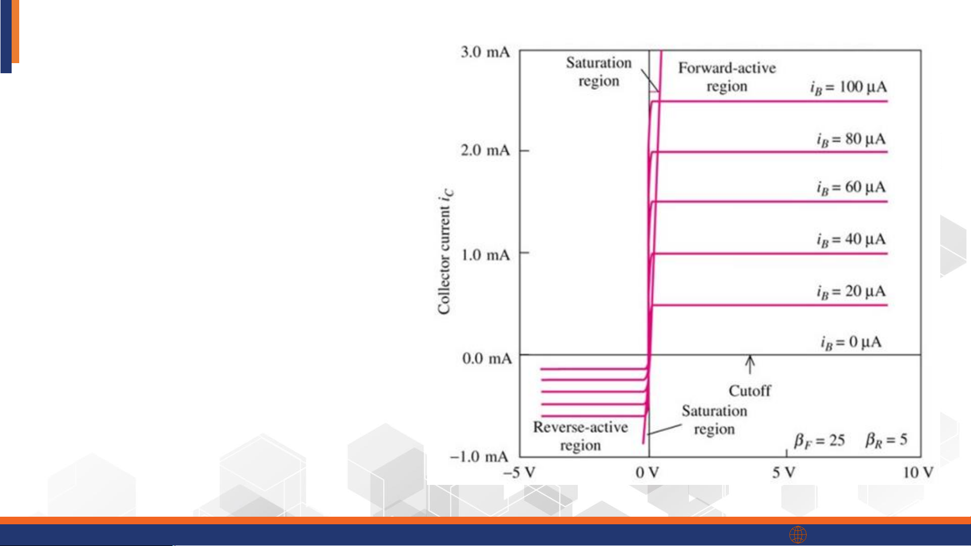
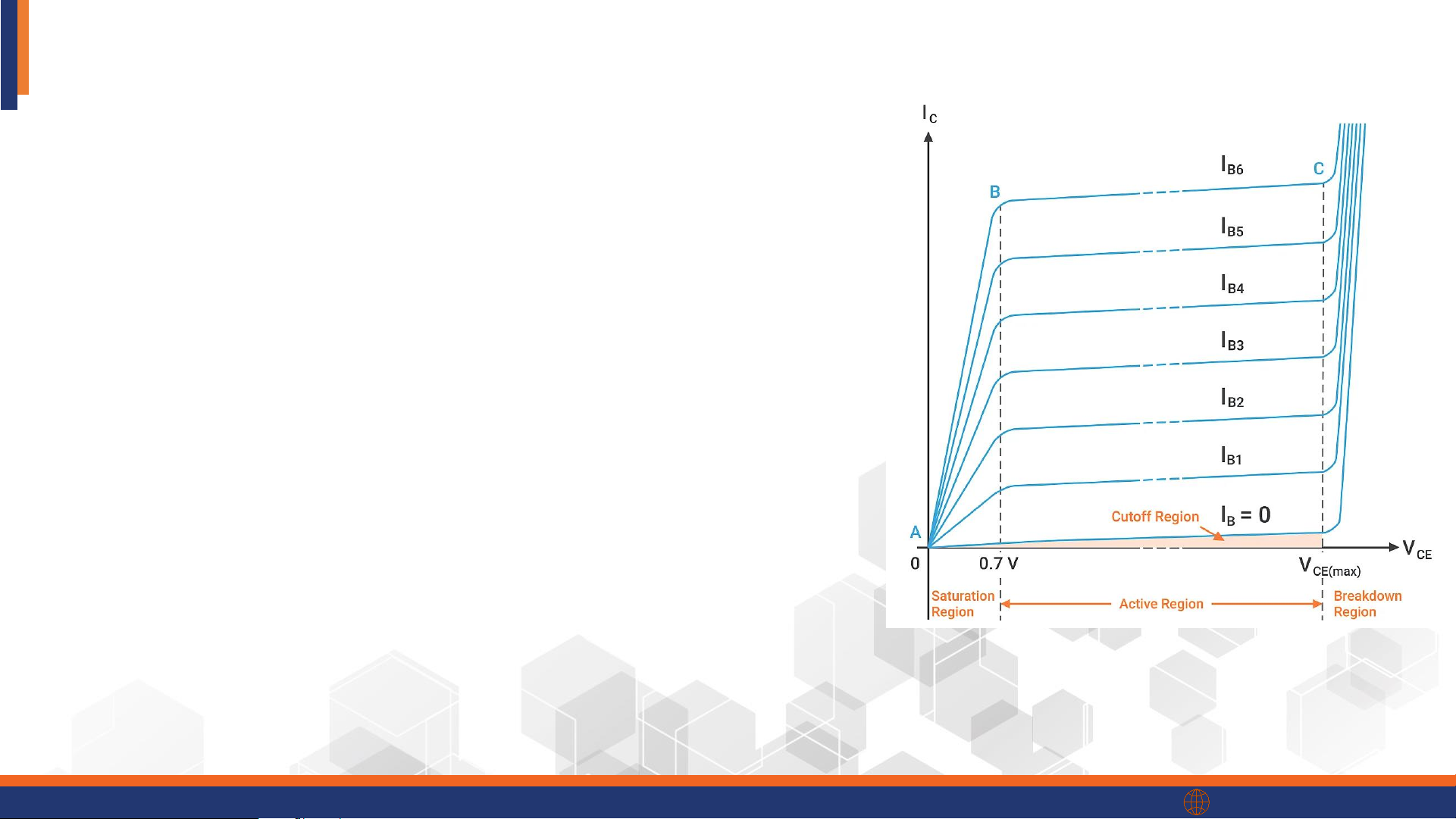
III.3. BJT Characteristics and Parameters
Collector Characteristic Curve
(Output characteristic curve for CE configuration):
IC vs VCE, for specified values of IB
• VB= 0.7 V, VCC =0, and VE=VC=0
→ BE junction and BC junction are forward-biased
→ Saturation region: VCC is increased,
VCE increases as the IC increases.
• When VCE exceeds 0.7 V, the BC junction becomes reverse-biased → Active region
• When VCE is too high, the BE junction is breakdown → Breakdown region phenikaa-uni.edu.vn