công nghệ bán dẫn Chapter 4_Field Effect Transistors


Preview text:
Faculty of Electrical and Electronic Engineering
Semiconductor Technology Dr. Le Viet Thong
Email: thong.leviet@phenikaa-uni.edu.vn phenikaa-uni.edu.vn
Chapter IV : FIELD-EFFECT TRANSISTORS Contents: IV.1. The JFET
IV.2. The JFET Characteristics and Parameters IV.3. JFET Biasing IV.4. The Ohmic Region of JFET IV.5. The MOSFET
IV.6. MOSFET Characteristics and Parameters IV.7. MOSFET Biasing IV.8. The IGBT IV.9. Troubleshooting phenikaa-uni.edu.vn Goals
• Understand the Structure and Operation of JFETs
• Discuss how JFETs differs from the BJT
• Study important JFETs parameters and characteristic curves
• How to bias JFETs and Analyze simple JFET circuits
• Discuss the Ohmic region on a JFET characteristic curve phenikaa-uni.edu.vn Goals
• Understand the Structure and Operation of MOSFETs
• Explore the differences between D-MOSFET and E-MOSFET
• Study important MOSFETs parameters and characteristic curves
• How to bias MOSFETs and Analyze simple MOSFET circuits
• Explore the structure and operation of insulated-gate bipolar transistor (IGBT). phenikaa-uni.edu.vn New words
Field – effect transistor Transistor hiệu ứng trường
Drain Cực máng
Source Cực nguồn
Gate Cực cổng
Enhancement mode Chế độ tăng cường
Depletion mode Chế độ làm nghèo
Cut-off Ngắt (dòng điện)
Pinch-off Thắt lại hoặc làm hẹp (dòng điện)
Saturation Bão hòa phenikaa-uni.edu.vn Introduction
• BJT is a current-controlled device; that is, the base current IB controls
the amount of collector current IC.
• A FET is a voltage-controlled device, where the voltages control the
current through the device (ID).
• A major advantage of FETs is their very high input resistance.
• FETs are not as widely used in amplifiers as BJTs. However, FETs are the
preferred device in low voltage switching applications because they are
generally faster than BJTs when turned on and off.
• The IGBT is a combination version of FETs and BJTs, and generally used in
high-voltage switching applications. phenikaa-uni.edu.vn
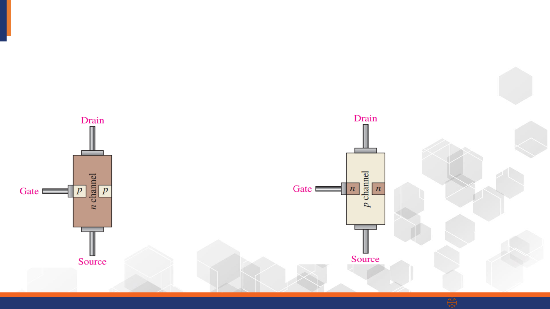
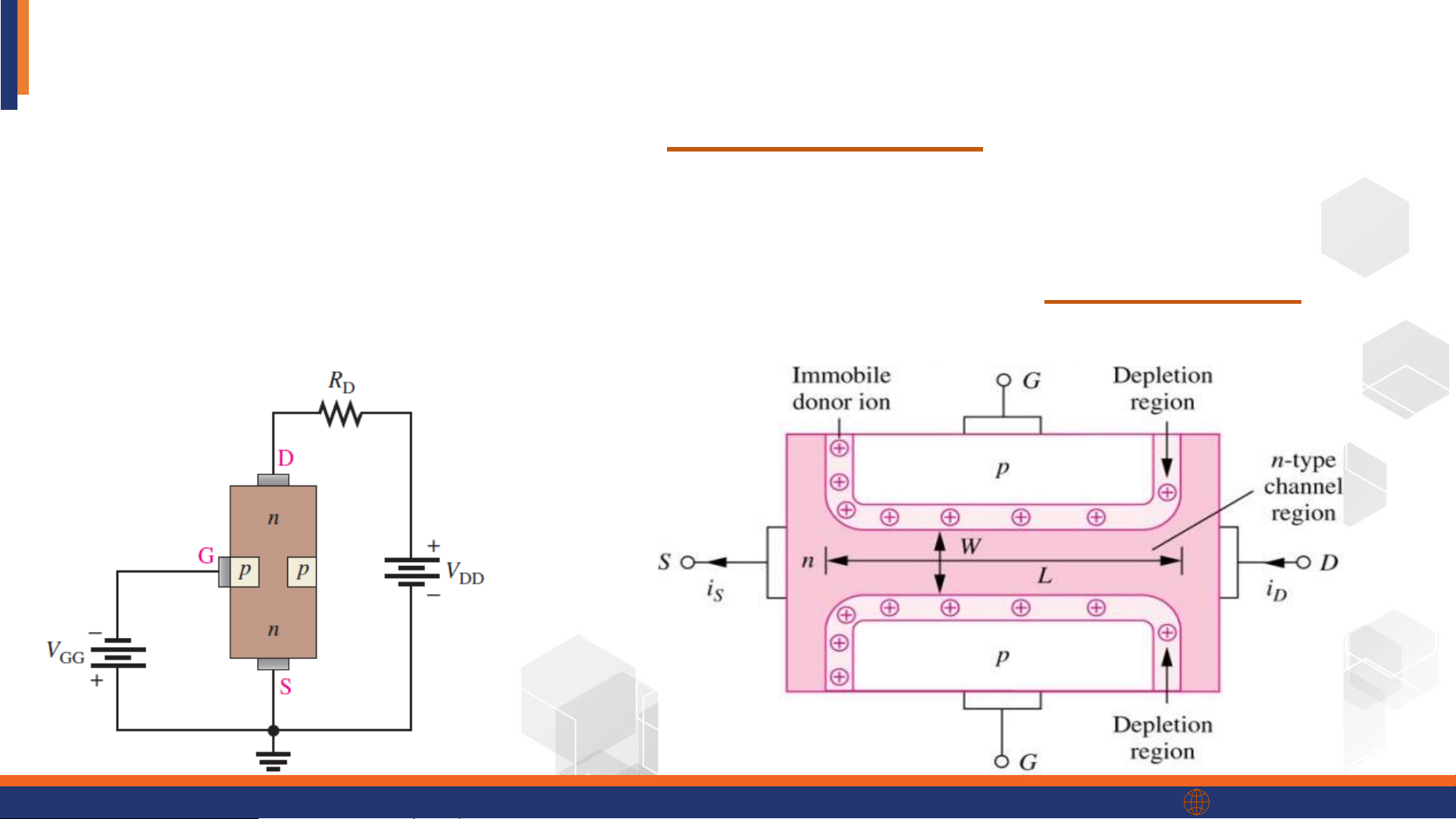
IV.1. The JFET (Junction Field effect transistor) The JFET – Structure
• Three terminals: Gate (G), Drain (D) at the upper end, and Source (S) at the lower
end. A channel is created to connect D and S.
• Two types: n-channel JFET and p-channel JFET
n-channel JFET: two
p-channel JFET: two p-type regions are n-type regions are connected to the Gate. connected to the Gate.
• Note: Two PN junctions are formed between the Gate and the channel. phenikaa-uni.edu.vn IV.1. The JFET The JFET – Symbols
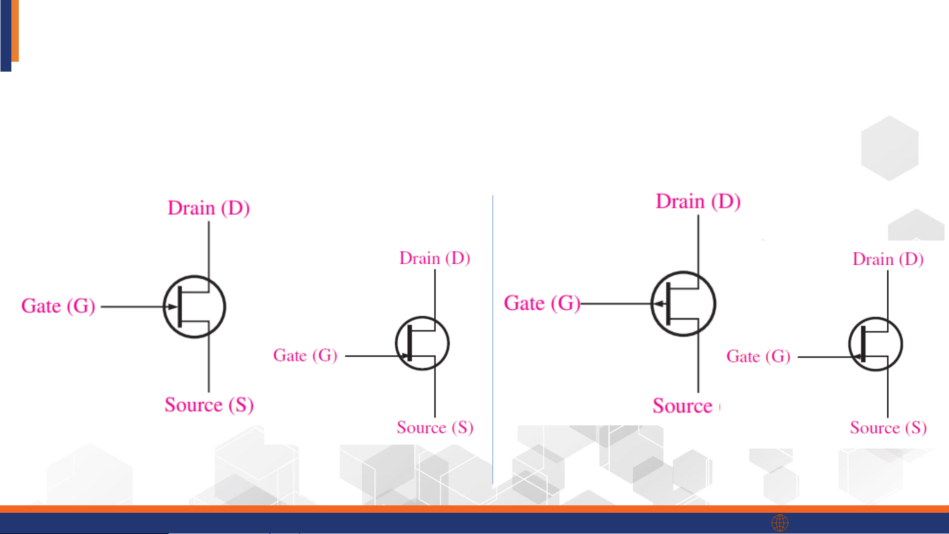
• The arrow is at the Gate
• Direction of the arrow indicates the PN junctions: From P → to N n-channel JFET p-channel JFET phenikaa-uni.edu.vn IV.1. The JFET
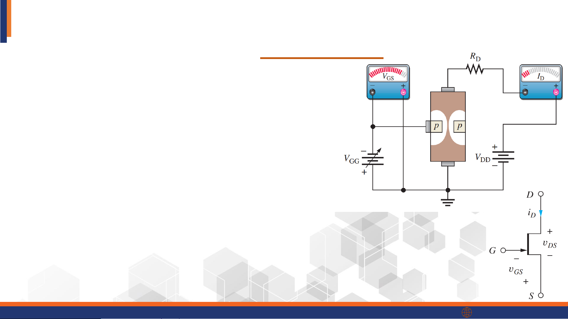
The JFET – Basic Operation of n-channel JFET
• JFET uses voltage to control the current flow
• VDD supplies current from Drain to Source (VDS>0).
• JFETs is always operated with Gate-Source pn junction reverse-biased.
• The current (ID) is controlled by the reverse-biased VGS and VDS. phenikaa-uni.edu.vn IV.1. The JFET
The JFET – Basic Operation of n-channel JFET ❖ VGS controls ID • VGS = 0:
Gate isolated from channel. If VDS > 0, there is a current flow (ID>0).
• VP < VGS < 0:
The depletion width increases due to the
reverse-biased gate-source junction. Channel
resistance increases, and ID decreases.
• VGS = VGS(off) < 0:
Channel is totally closed. Channel resistance
is infinite, and ID=0. VGS(off) is cutoff voltage. phenikaa-uni.edu.vn IV.1. The JFET
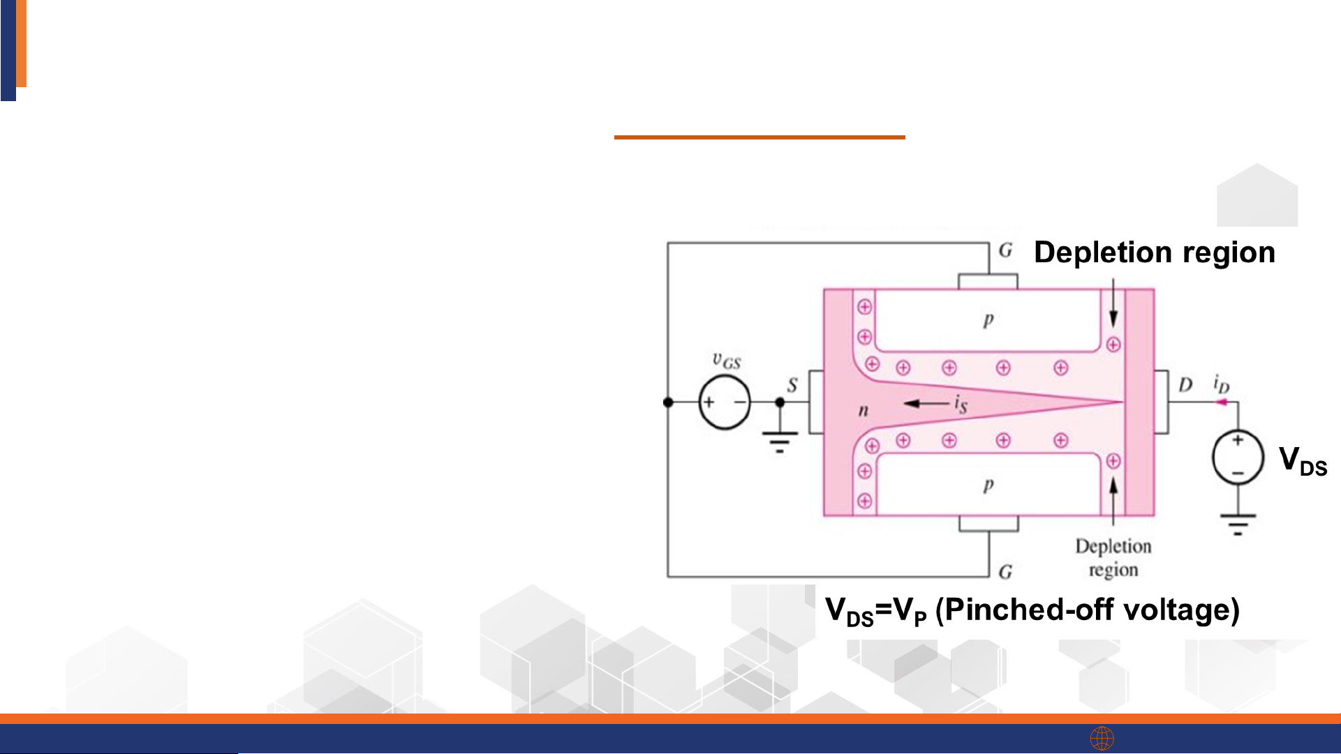
The JFET – Basic Operation of n-channel JFET
• For a value of VGS in range of (VGS(off) < VGS ≤ 0): ID also depend on VDS (VDS >0) • For a small VDS :
ID increase with the increase in VDS (regarding the Ohm law)
• When VDS ≥ VP > 0 :
Depletion region near drain increases
→ The channel is totally pinched-off
→ ID is saturated (IDSS)
• When VDS is too high, the pn junctions are breakdown phenikaa-uni.edu.vn IV.1. The JFET
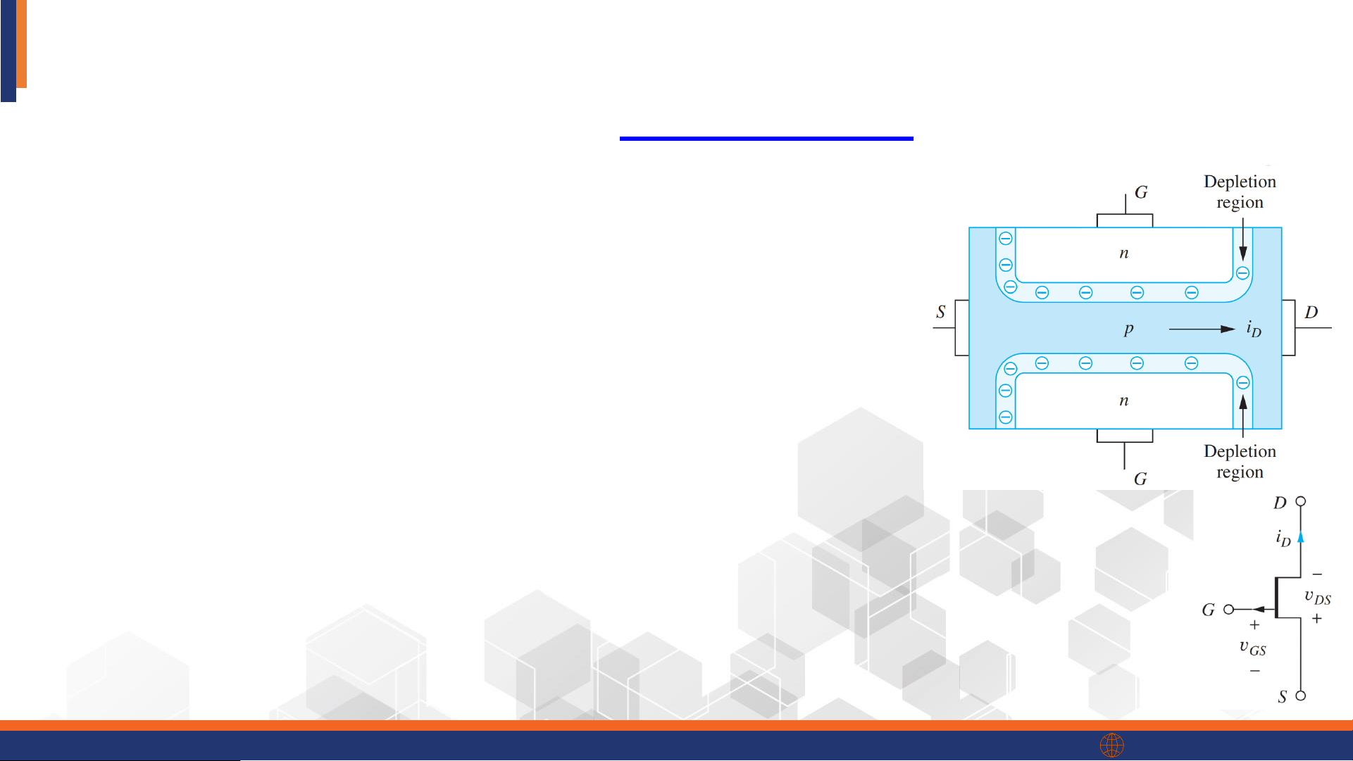
The JFET – Basic Operation of p-channel JFET
Channel current direction and operating bias voltages are reversed.
• VGS = 0: If VDS < 0, there is a current flow (ID>0)
• 0 < VGS < VGS(off) : ID decreases
• VGS > VGS(off) > 0 : ID=0
• For a value of VGS in range of (0 ≤ VGS < VGS(off) ):
ID depend on VDS (VDS<0)
- For a small VDS : ID increase with the increase in |VDS|
- When VDS ≤ VP < 0 : Depletion region near drain increases
→ The channel is totally pinched-off → ID is saturated (IDSS)
- When VDS is too negative, the pn junctions are breakdown phenikaa-uni.edu.vn
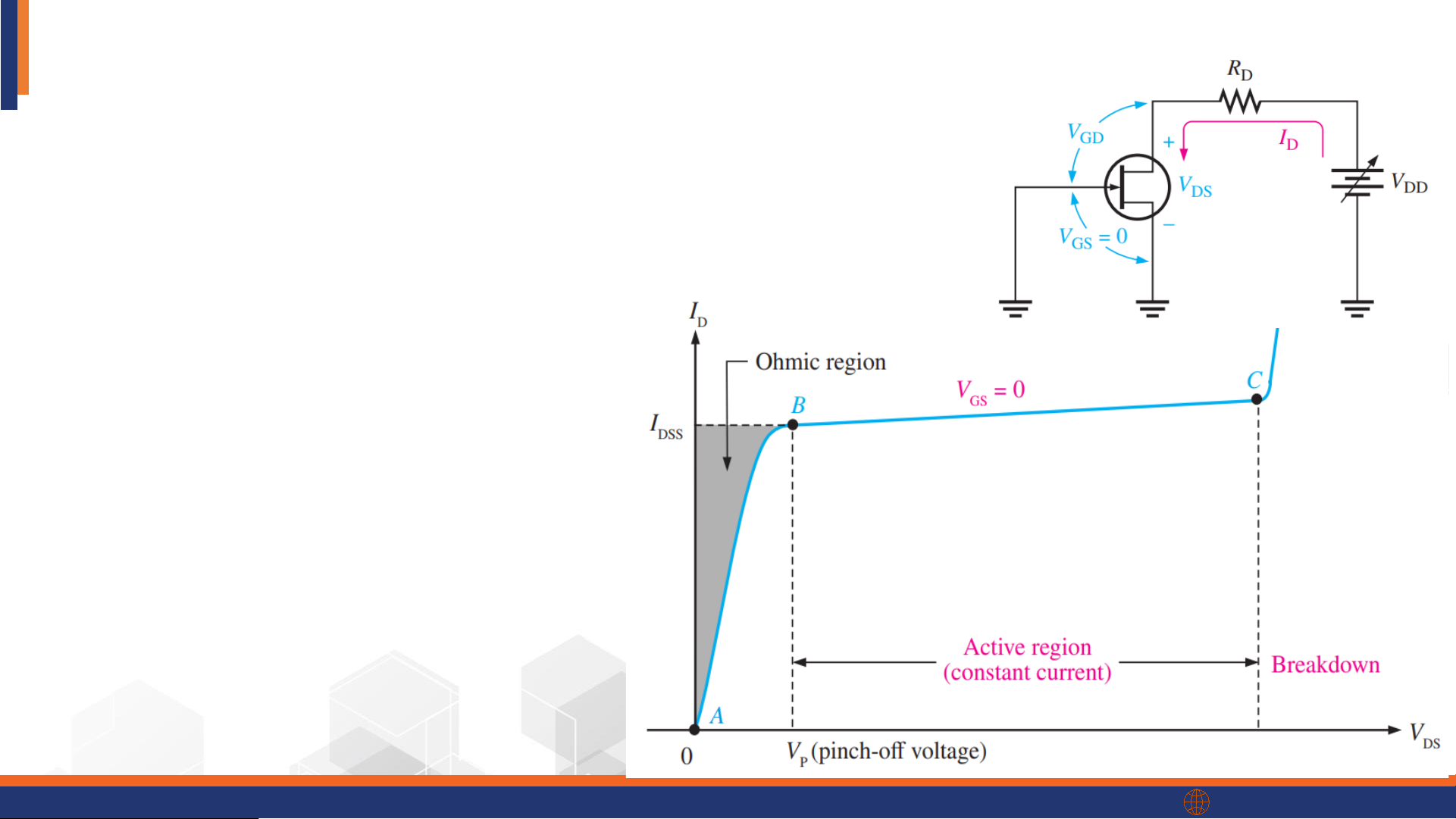
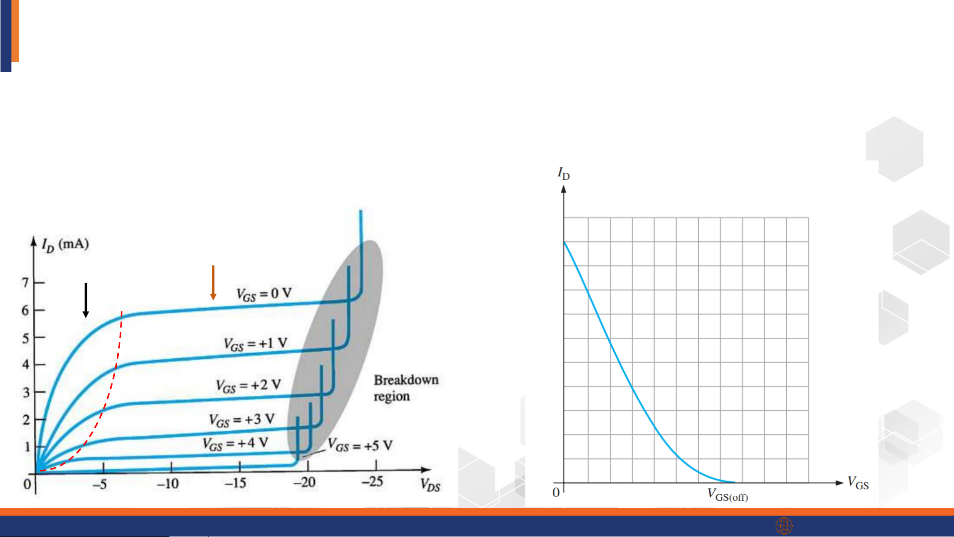
IV.2. The JFET Characteristics and Parameters
Drain Characteristic Curve (n-channel): ID vs VDS
When VGS = 0 V:
Drain characteristic Curve has three regions:
• Ohmic region (A to B): current and
voltage are related by Ohm’s law.
• Active (or constant-current)
region (B to C): where current is independent of VDS.
• Breakdown region (beyond C): Operation in this region can damage the JFET. phenikaa-uni.edu.vn
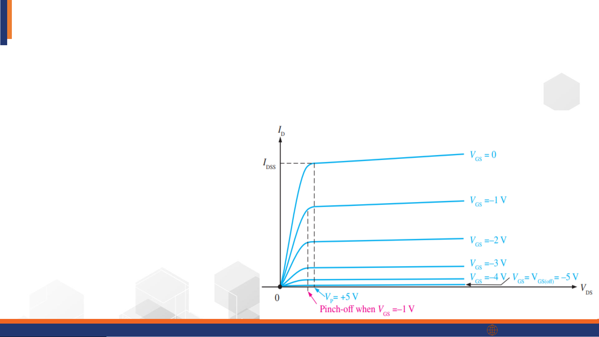
IV.2. The JFET Characteristics and Parameters
Drain Characteristic Curve (n-channel)
Reverse-bias VGS (When VGS <0): VGS controls ID
• ID decreases as the magnitude of VGS is increased to larger negative values
because of the narrowing of the channel.
• The value of VGS that makes ID=0
is the cutoff voltage (VGS(off)).
• VGS(off) = - VP (at VGS=0) phenikaa-uni.edu.vn
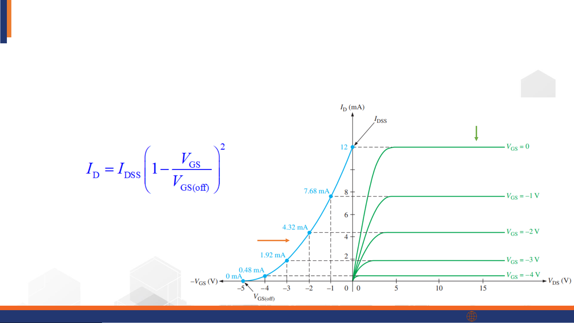
IV.2. The JFET Characteristics and Parameters
Transfer Characteristic Curve (n-channel): ID vs VGS
• The transfer curve is a is a plot of the output current (ID) to the input voltage
(VGS) from cutoff (VGS(off) ) to pinch-off (VP). Drain Characteristic
• The transfer curve is based on the equation: Curve
IDSS is the saturation value of ID at VGS =0 Transfer Characteristic Curve phenikaa-uni.edu.vn
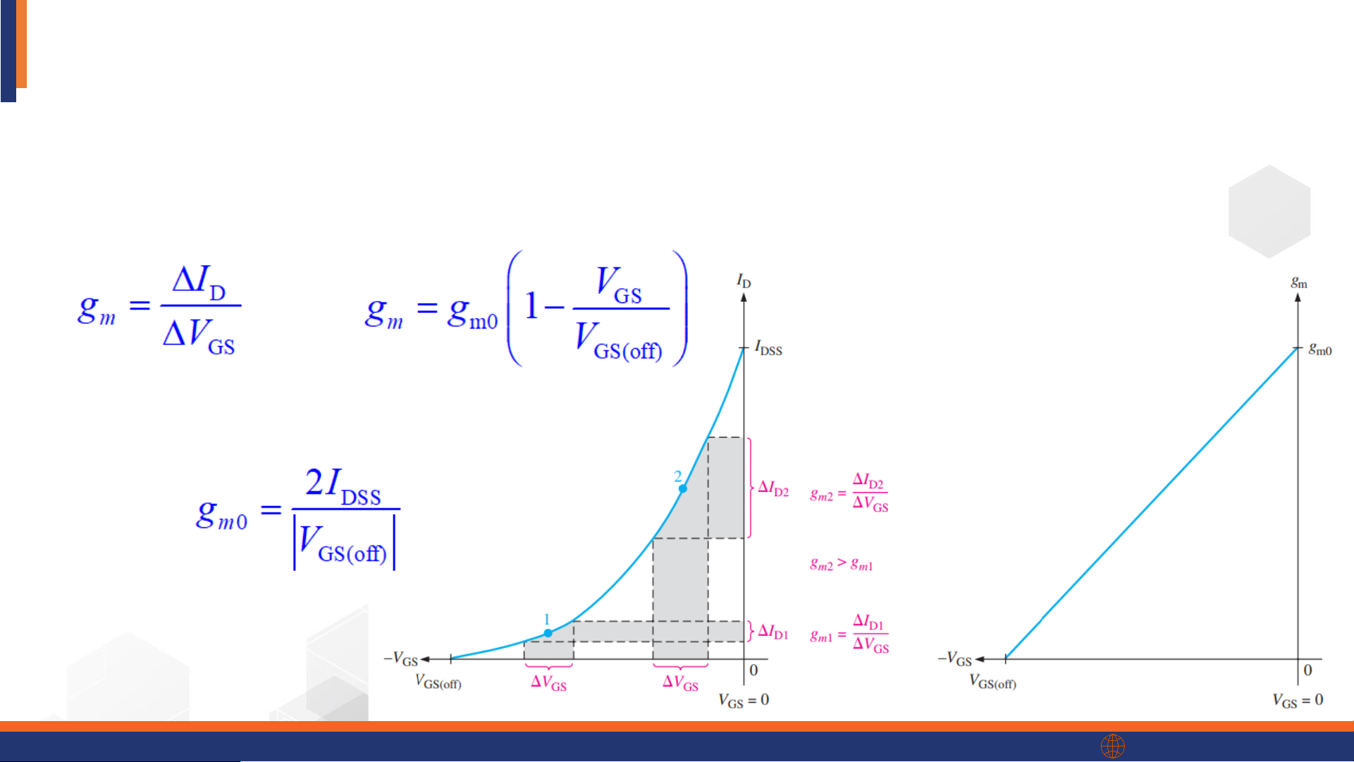
IV.2. The JFET Characteristics and Parameters
Forward Transconductance (n-channel) (Độ hỗ dẫn)
• The forward transconductance (gm) is the ratio of a change in output current (ΔID)
to a change in the input voltage (Δ VGS).
• The value of gm0 can be found as: phenikaa-uni.edu.vn
IV.2. The JFET Characteristics and Parameters
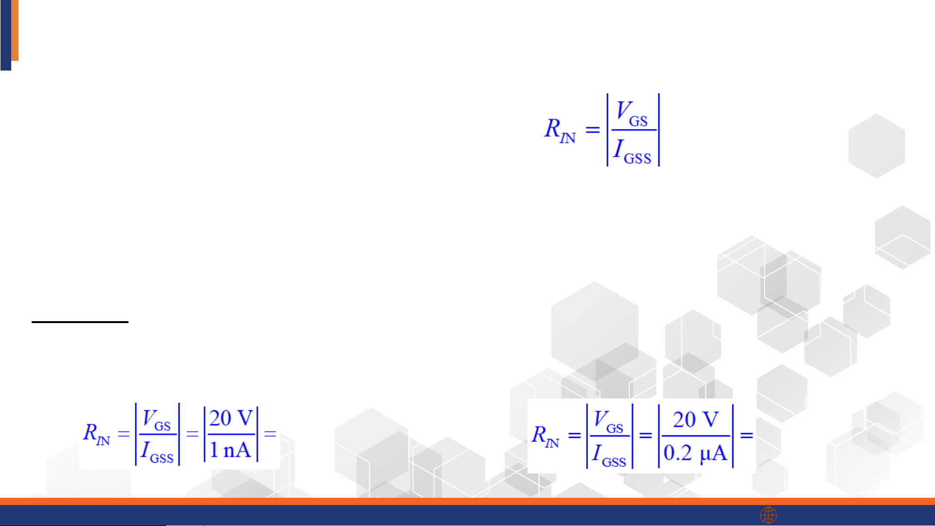
Input Resistance (n-channel)
• The input resistance of a JFET is given by:
where IGSS is the current into the reverse biased gate.
• JFETs have very high input resistance, but it drops when the temperature increases.
Example: The data sheet of a 2N5485 shows that for VGS = -20 V, IGSS = 1 nA at 25 oC
and 0.2 mA at 100 oC. Compare the input resistance at 25 oC and at 100 oC At 25 oC, At 100 oC, 20 G 100 M phenikaa-uni.edu.vn
IV.2. The JFET Characteristics and Parameters
JFET p-channel Characteristic Curves
• The characteristic curves of p-channel JFET are the mirror image of n-channel JFET
curves. Channel current direction and operating bias voltages are also reversed. Drain Characteristic Curve
of p-channel JFET Active region Ohmic region Transfer Characteristic
Curve of p-channel JFET phenikaa-uni.edu.vn IV.3. JFET Biasing
• The purpose of biasing is to select the proper dc Gate-Source voltage to
establish a desired value of drain current ID and a proper Q-point.
• The 2 main ways to bias a JFET are self-bias and voltage-divider bias.
• The VGS will be negative for n-channel JFET (positive for p-channel JFET)
to keep the GS junction reverse biased. phenikaa-uni.edu.vn IV.3. JFET Biasing
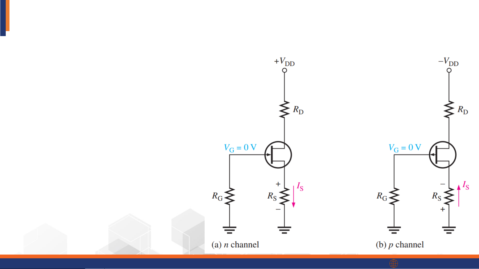
Self-bias (VG=0) is simple and effective method for JFET
For all JFET circuits: ID = IS
(n channel) VGS = VG – VS = - IDRS
(p channel) VGS = +IDRS VD = VDD – IDRD VDS = VD – VS = VDD – ID(RD + RS) where VS = IDRS phenikaa-uni.edu.vn