Final Report Môn Computer Architecture and Organization Lab | Đại học Sư phạm Kỹ thuật Thành phố Hồ Chí Minh
Final Report Môn Computer Architecture and Organization Lab. Tài liệu được sưu tầm gồm 71 trang, giúp bạn ôn tập tốt hơn. Mời các bạn đón xem.
Môn: Computer Architecture and Organization Lab (COOL325364E) 10 tài liệu
Trường: Trường Đại học Sư phạm Kỹ thuật Thành phố Hồ Chí Minh 4.4 K tài liệu
Tác giả:


Preview text:
lOMoAR cPSD| 58583460
HCMC UNIVERSITY OF TECHNOLOGY AND EDUCATION
FACULTY FOR HIGH QUALITY TRAINING SUBJECT
Computer Architecture and Organization Lab FINALREPORT Lecturer:
Student: Le Thi Kieu Giang 19119001
Course ID: COOL325364E-02CLC HCM City, 12/2021 lOMoAR cPSD| 58583460 TABLE OF CONTENTS
TABLE OF CONTENTS ................................................................................................. 1 TABLE OF FIGURES
..................................................................................................... 4
PART A: 8086 MPU ........................................................................................................ 6
WEEK 1 and WEEK 2:..............................................................................................7 I. Objective
...........................................................................................................7 II. Requirements
...................................................................................................7 III. Design and Implementation
...........................................................................7IV. Results (code &
schematic) ........................................................................... 7 V. Discuss
.............................................................................................................9 WEEK 3:
...................................................................................................................10 I.
Objective .........................................................................................................10 II. Requirements
.................................................................................................10 III. Design and Implementation
.........................................................................10IV. Results (code &
schematic) ......................................................................... 10 V. Discuss
...........................................................................................................14 WEEK 4:
...................................................................................................................15 I.
Objective .........................................................................................................15 II. Requirements
.................................................................................................15 lOMoAR cPSD| 58583460 III. Design and Implementation
.........................................................................15IV. Results (code &
schematic) ......................................................................... 15 V. Discuss
...........................................................................................................18 WEEK 5:
...................................................................................................................19 I.
Objective .........................................................................................................19 II. Requirements
.................................................................................................19 III. Design and Implementation
.........................................................................19IV. Results (code &
schematic) ......................................................................... 19 V. Discuss
...........................................................................................................22 WEEK 6:
...................................................................................................................23 I. Objective
.........................................................................................................23 II. Requirements
.................................................................................................23 III. Design and Implementation
.........................................................................23IV. Results (code &
schematic) ......................................................................... 23 V. Discuss
...........................................................................................................26
WEEK 7: ...................................................................................................................27
I. Objective .........................................................................................................27
II. Requirements .................................................................................................27 III. Design and Implementation
.........................................................................27IV. Results (code &
schematic) ......................................................................... 27 V. Discuss
...........................................................................................................29 lOMoAR cPSD| 58583460
PART B: 8051 MCU ...................................................................................................... 30
WEEK 8: ...................................................................................................................31
I. Objective .........................................................................................................31
II. Requirements .................................................................................................31 III. Design and Implementation
.........................................................................31IV. Results (code &
schematic) ......................................................................... 31 V. Discuss
...........................................................................................................34
WEEK 9: ...................................................................................................................35
I. Objective .........................................................................................................35
II. Requirements .................................................................................................35 III. Design and Implementation
.........................................................................35IV. Results (code &
schematic) ......................................................................... 35 V. Discuss
...........................................................................................................37
WEEK 10: ................................................................................................................ 38
I. Objective .........................................................................................................38
II. Requirements .................................................................................................38 III. Design and Implementation
.........................................................................38IV. Results (code &
schematic) ......................................................................... 38 V. Discuss
...........................................................................................................40
PART C: HIGH-LEVEL PROGRAMMING ON AT89C51 ........................................41
WEEK 11: ................................................................................................................ 42 I.
Objective .........................................................................................................42
II. Requirements .................................................................................................42 lOMoAR cPSD| 58583460 III. Design and Implementation
.........................................................................42IV. Results (code &
schematic) ......................................................................... 42 V. Discuss
...........................................................................................................52
WEEK 12: ................................................................................................................ 54
I. Objective .........................................................................................................54
II. Requirements .................................................................................................54 III. Design and Implementation
.........................................................................54IV. Results (code &
schematic) ......................................................................... 54 V. Discuss
...........................................................................................................61
WEEK 13: ................................................................................................................ 62
I. Objective .........................................................................................................62
II. Requirements .................................................................................................62 III. Design and Implementation
.........................................................................62IV. Results (code &
schematic) ......................................................................... 63 V. Discuss
...........................................................................................................66
WEEK 14: ................................................................................................................ 67
I. Objective .........................................................................................................67
II. Requirements .................................................................................................67 III. Design and Implementation
.........................................................................67IV. Results (code &
schematic) ......................................................................... 68
V. Discuss ...........................................................................................................70
REFERENCES ............................................................................................................... 71 TABLE OF FIGURES lOMoAR cPSD| 58583460
Figure: Addition and Subtraction 2 numbers ...................................................................8 Figure: Covert 2 numbers
.................................................................................................9 Figure: Storage addition
of 8-bits register ..................................................................... 12
Figure: Survey instructions such as JMP,JLE and label ................................................13
Figure: Decrease/increase variable value .......................................................................14
Figure: Add and subtract 2 numbers have 2-digits. .......................................................17
Figure: Enter 5 digit numbers from keyboard ................................................................18
Figure: Calculate and storage a 5 digit numbers into a 16-bit register ..........................21
Figure: Enter n bit from keyboard and print exponential 2 ........................................... 22
Figure: Survey Shift 8-bit registers ................................................................................ 24
Figure: Survey Shift 8-bit registers ................................................................................ 26
Figure: Change binary to decimal and print on the screen ............................................ 28
Figure: Change decimal to binary and print on the screen ............................................ 29
Figure: Addition 2 number in 7-segment LED display ................................................. 32
Figure: P2.7 equals 1, Add 2 numbers. .......................................................................... 34
Figure: P2.7 equals 0, Subtract 2 numbers.....................................................................34
Figure : Calculating frequency and duty cycle in the first problem. .............................35
Figure : Frequency and duty cycle of second problem. .................................................36
Figure: Display 7-segment LED by 2Hz ........................................................................39
Figure: Alternating blinking LED ..................................................................................43
Figure : Single LED interface with latch circuit ............................................................45 Figure: Design 7-segment LED
......................................................................................47
Figure: Display 7-segment LED by IC 74LS247 Decoder ............................................48
Figure: Display 7-segments LED by scan method ........................................................ 50
Figure: Scanning 7-segment LED by IC 74245 .............................................................52
Figure: AT89C51 and Button .........................................................................................55
Figure: AT89C51 and Switch .........................................................................................56
Figure: Using interrupts to check state when single LED is changed ...........................57 lOMoAR cPSD| 58583460
Figure: Using external interrupt to increase the value of LED ......................................59
Figure: Creating precise delay using Timer/Interrupt ....................................................60
Figure: Analog Channel Selection ................................................................................. 62 Figure: Time diagram
..................................................................................................... 62 Figure: Analog to
digital converter ADC ...................................................................... 63
Figure: 8 the sensor temperature LM35 to measure temperature ..................................65
Figure: Virtual Serial Port Driver Software...................................................................67 Figure: H-Term.
..............................................................................................................68 Figure: UART
application ..............................................................................................69 lOMoAR cPSD| 58583460 PART A: 8086 MPU
The general purpose of this section is to help learners review some of the issues of
computer architecture from using the design of a computer. In addition, the supported
instruction set architectures for this family of microcontrollers are briefly outlined.
Help learners manipulate the commands supported in the script.
Examine assembly language and the meaning of the process of compiling source code into machine code.
From the basic examples, learners can understand in-depth the usage of each
instruction code, the structure and influence of the registers, as well as the control programming methods such as:
- Move and exchange data, sort, exchange and find elements in arrays.
- Arithmetic processing such as addition, subtraction, multiplication, division Logical processing. - HEX and BCD counters.
- Convert BCD, DEC, HEX digital system. lOMoAR cPSD| 58583460 WEEK 1 and WEEK 2: I. Objective
Learn about Assembly language. Understand basic registers.
Understand and use MOV, INT, ADD and SUB instructions. II. Requirements
Can use MOV and INT instructions. Study the ADD and SUB instructions and solve the problem.
Enter two 1-digit numbers from the keyboard in which the first number is larger than
the second one. Calculate the addition and subtraction of them. Algorithm:
- ADD: operand1 = operand1 + operand2.
- SUB: operand1 = operand1 - operand2.
III. Design and Implementation
We use 2 instructions as ADD and SUB to solve the requirement.
After the calculation of results from problem 1, we will change these results into numbers.
IV. Results (code & schematic)
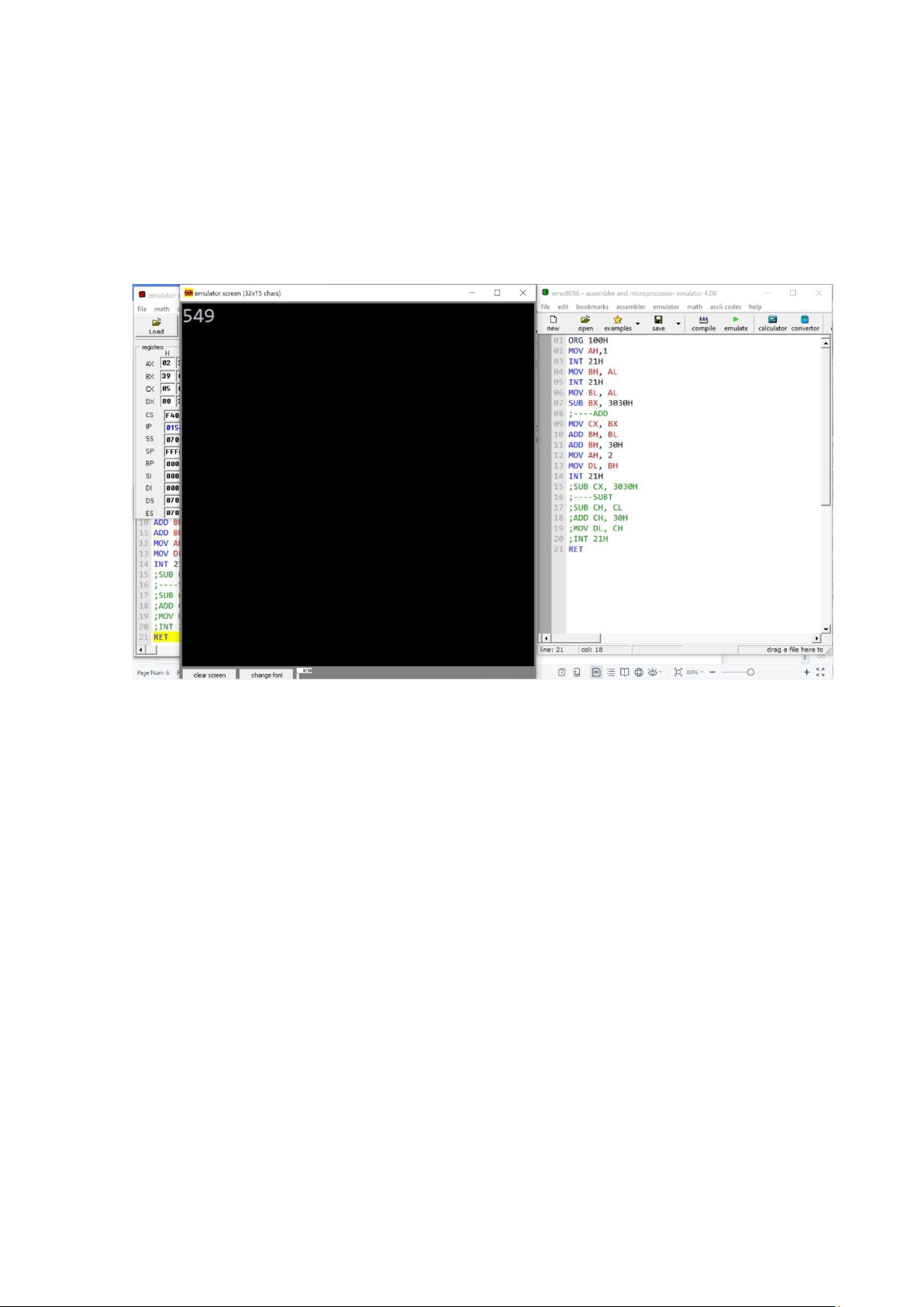
Problem 1: Addition and Subtraction 2 numbers Code: ORG 100H MOV AH,1 INT 21H MOV BH, AL INT 21H MOV BL, AL SUB BX, 3030H ;----ADD MOV CX, BX ADD BH, BL ADD BH, 30H MOV AH, 2 MOV DL, BH INT 21H ;SUB CX, 3030H lOMoAR cPSD| 58583460 ;----SUBT SUB CH, CL ADD CH, 30H MOV DL, CH INT 21H RET Solution:
Figure: Addition and Subtraction 2 numbers
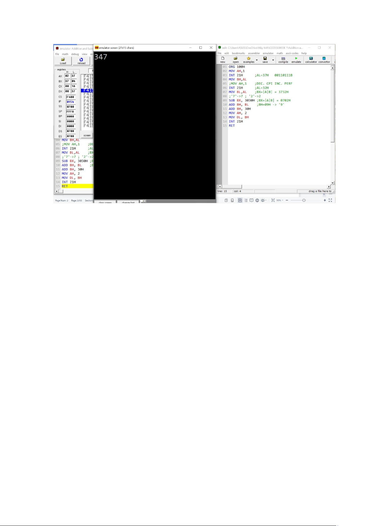
Problem 2: Covert 2 numbers Code: ORG 100H MOV AH,1 INT 21H ;AL=37H 00110111B MOV BH,AL ;MOV AH,1 ;DEC. CPI INC. PERF INT 21H ;AL=32H MOV BL,AL ;BX=|A|B| = 3732H ;'7'->7 ; '2'->2
SUB BX, 3030H ;BX=|A|B| = 0702H ADD BH, BL ;BH=09H -> '9' ADD BH, 30H MOV AH, 2 MOV DL, BH INT 21H RET Solution: lOMoAR cPSD| 58583460
Figure: Covert 2 numbers V. Discuss
Understanding Assembly programming language.
Understand and use basic registers.
After the problem, we can fluently use the MOV, INT, SUB, ADD instructions.
Moreover, we can fluently use the SUB and ADD instructions and convert numbers to
characters and characters to numbers. WEEK 3: I. Objective
Help learners continue to solve problems using ADD and SUB instruction.
Know is to store the execution result in an 8-bit register. Know how to use labels. II. Requirements
Solve the problem of "Input 2 digits and store in 8-bit register".
III. Design and Implementation
We will use last week's design to solve the question of "Input 2 digits and store in 8-bit register".
Store in 8-bit register using tenth division. lOMoAR cPSD| 58583460
In this problem, we will examine the branch instruction and label structure to solve
the problem of storing in 8-bit registers.
IV. Results (code & schematic)
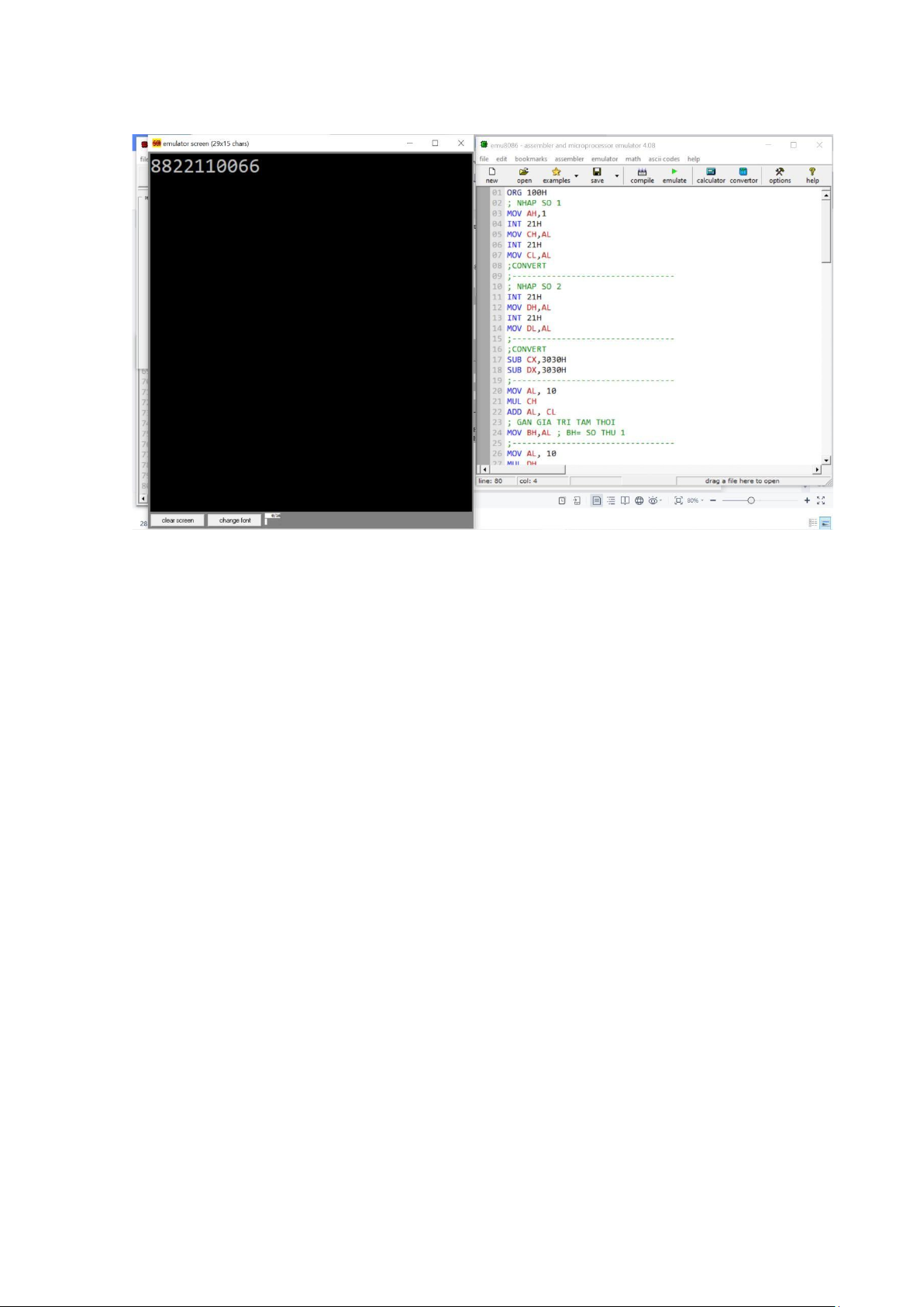
Problem 1: Storage addition of 8-bits register Code: ORG 100H ; NHAP SO 1 MOV AH,1 INT 21H MOV CH,AL INT 21H MOV CL,AL ;CONVERT
;--------------------------------- ; NHAP SO 2 INT 21H MOV DH,AL INT 21H MOV DL,AL
;--------------------------------- ;CONVERT SUB CX,3030H SUB DX,3030H
;--------------------------------MOV AL, 10 MUL CH ADD AL, CL ; GAN GIA TRI TAM THOI MOV BH,AL ; BH= SO THU 1
;--------------------------------MOV AL, 10 MUL DH ADD AL, DL ; GAN GIA TRI TAM THOI MOV BL,AL ; BL = SO THU 2
;--------------------------------MOV CX,BX ;PHEP TINH ADD/SUB ADD BH,BL ; CONG BH=BH+BL ;ADD BL,BH ; CONG BL=BH+BL ;MOV AL,BH lOMoAR cPSD| 58583460
;--------------------------------SUB CH,CL ; CH=CH-CL ;MOV BL,CH ; GAN BL = CH
;--------------------------------; PHEP CONG MOV AL,BH MOV DL,10 DIV DL MOV BL,AH MOV AH,0 DIV DL ;-------------------------MOV CL,AH MOV AH,2 MOV DL,AL ADD DL,30H INT 21H MOV DL,CL ADD DL,30H INT 21H MOV DL,BL ADD DL,30H INT 21H ; PHEP TRU MOV AX,0H MOV AL,CH MOV DL,10 DIV DL MOV BL,AH MOV AH,0 DIV DL ;-----------------------MOV CL,AH MOV AH,2 MOV DL,AL ADD DL,30H INT 21H MOV DL,CL ADD DL,30H INT 21H MOV DL,BL ADD DL,30H INT 21H RET lOMoAR cPSD| 58583460 Solution:
Figure: Storage addition of 8-bits register
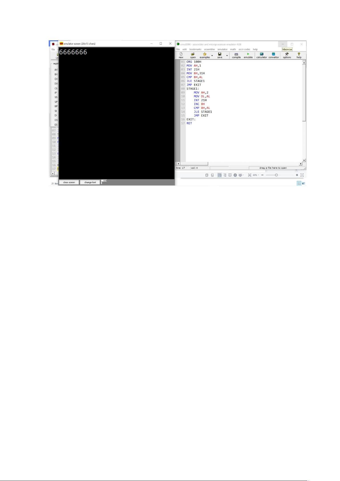
Problem 2: Survey instructions such as JMP,JLE and label. Code: ORG 100H MOV AH,1 INT 21H MOV BH,31H CMP BH,AL JLE STAGE1 JMP EXIT STAGE1: MOV AH,2 MOV DL,AL INT 21H INC BH CMP BH,AL JLE STAGE1 JMP EXIT EXIT: RET Solution: lOMoAR cPSD| 58583460
Figure: Survey instructions such as JMP,JLE and label
Problem 3: Applying branching structure to decrease/increase variable value Code: ORG 100H MOV AH,1 INT 21H CMP AL,35H JG DECCASE JLE INCCASE DECCASE: CMP AL,30H JE EXIT DEC AL MOV AH,2 MOV DL,AL INT 21H JGE DECCASE INCCASE: CMP AL,39H JE EXIT INC AL MOV AH,2 MOV DL,AL INT 21H JGE INCCASE EXIT: RET lOMoAR cPSD| 58583460 Solution:
Figure: Decrease/increase variable value V. Discuss
We know how to store data in 8-bit registers and examine the principle of branching and label structures.
Understand and use labels well.
Sorting algorithm is more optimal. WEEK 4: I. Objective
Survey MUL and DIV instructions. II. Requirements
Study and can use MUL and DIV instructions to solve the problem. Algorithm: MUL:
- When operand is a byte: AX = AL * operand.
- When operand is a word: (DX AX) = AX * operand. DIV:
- When operand is a byte: AL = AX / operand. AH = remainder (modulus).
- When operand is a word: AX = (DX AX) / operand DX = remainder (modules).
III. Design and Implementation
Survey the MUL and DIV instructions.
Applying multiple and division solve the problems such as storing 0 to 4 digit
numbers in the 16-bit register and entering 5 digit numbers from Keyboard. lOMoAR cPSD| 58583460
IV. Results (code & schematic)
Problem 1: Enter 2 numbers have 2 digits. Calculate the addition and subtraction,
print the result to the screen. Code: ORG 100H ;1ST NUMBER MOV AH,1 INT 21H SUB AL,30H MOV DH,10 MUL DH MOV BL,AL MOV AH,1 INT 21H SUB AL,30H ADD BL,AL ;2ND NUMBER MOV AH,1 INT 21H SUB AL,30H MOV DH,10 MUL DH MOV BH,AL MOV AH,1 INT 21H SUB AL,30H ADD BH,AL ;TONG MOV AX,BX ADD AL,AH MOV AH,0 DIV DH MOV CL, AH MOV AH,0 DIV DH MOV DX,AX ;IN RA MAN HINH TONG MOV AH,2 ADD DL,30H INT 21H MOV DL,DH ADD DL,30H lOMoAR cPSD| 58583460 INT 21H MOV DL,CL ADD DL,30H INT 21H ;HIEU MOV AX,BX SUB AL,AH MOV DH,10 MOV AH,0 DIV DH MOV BX,AX ;IN RA MAN HINH HIEU MOV AH,2 MOV DL,BL ADD DL,30H INT 21H MOV DL,BH ADD DL,30H INT 21H RET Solution:
Figure: Add and subtract 2 numbers have 2-digits.
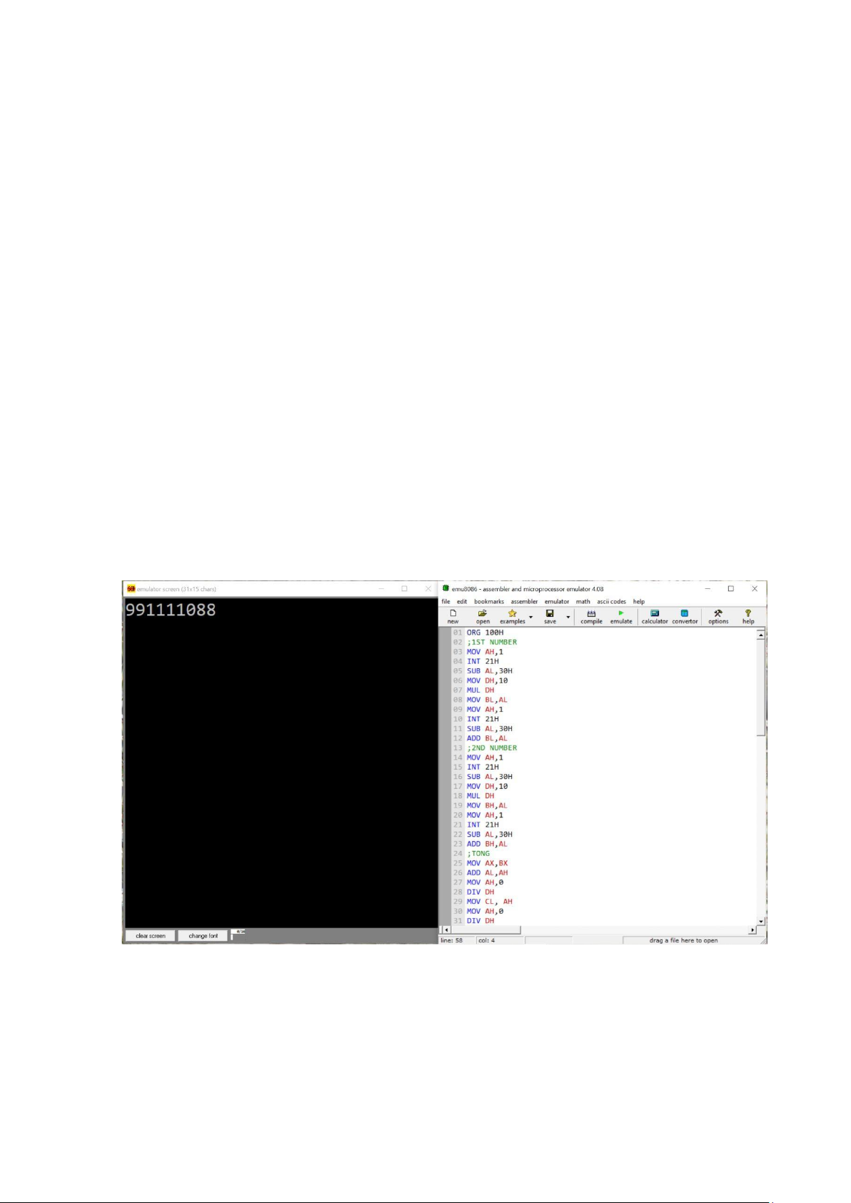
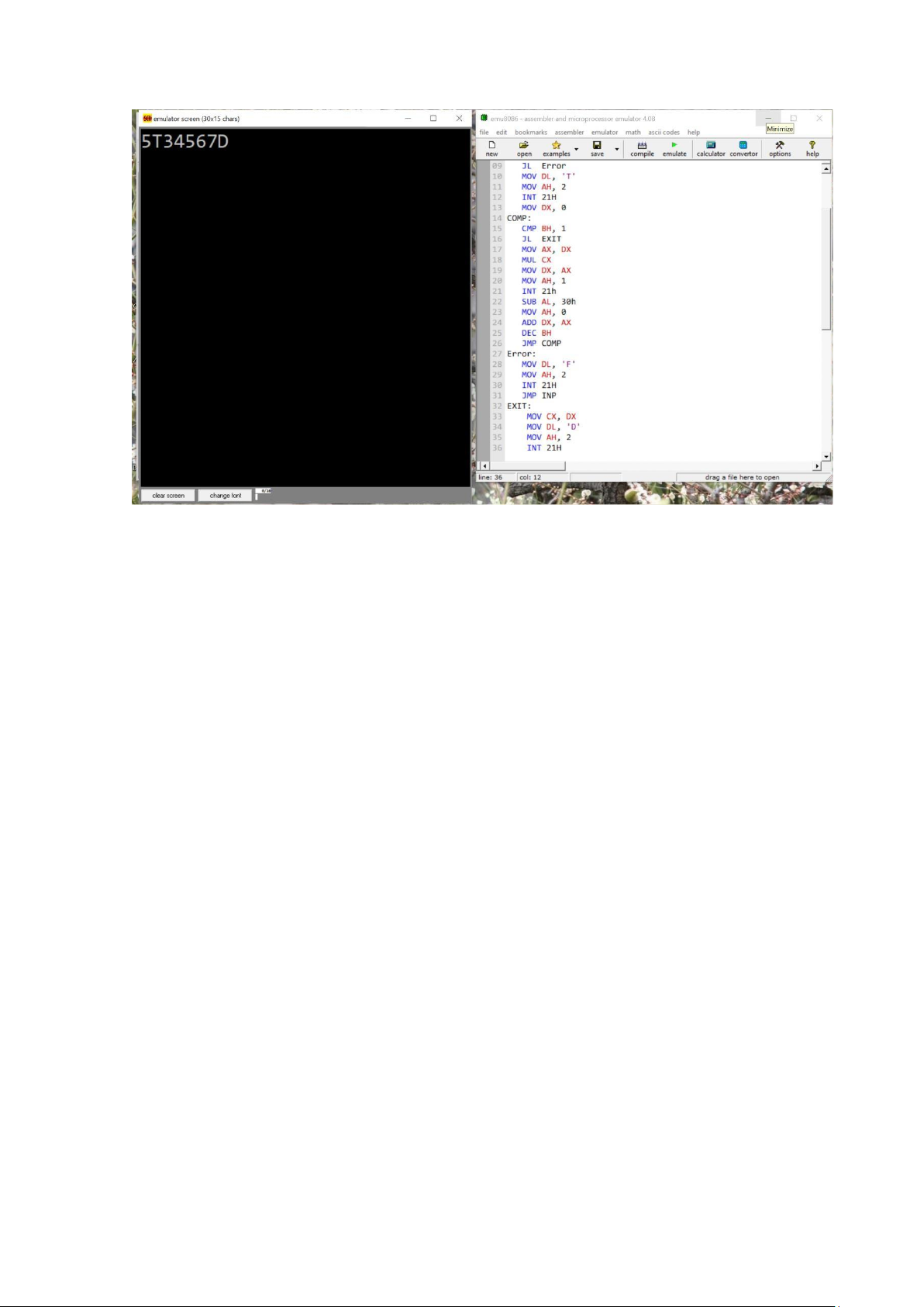
Problem 2: Enter 5 digit numbers from keyboard Code: MOV CX, 0AH INP: MOV AH, 1 INT 21h lOMoAR cPSD| 58583460 SUB AL, 30h MOV BH, AL CMP BH, 5h JG Error CMP BH, 1H JL Error MOV DL, 'T' MOV AH, 2 INT 21H MOV DX, 0 COMP: CMP BH, 1 JL EXIT MOV AX, DX MUL CX MOV DX, AX MOV AH, 1 INT 21h SUB AL, 30h MOV AH, 0 ADD DX, AX DEC BH JMP COMP Error: MOV DL, 'F' MOV AH, 2 INT 21H JMP INP EXIT: MOV CX, DX MOV DL, 'D' MOV AH, 2 INT 21H Solution: lOMoAR cPSD| 58583460
Figure: Enter 5 digit numbers from keyboard V. Discuss
We can understand how to use multiples and divides in Assembly to solve
questions. Furthermore, learners can design a basic math problem using a combination of instructions. WEEK 5: I. Objective
Introduction to POP and PUSH instructions.
Transfer memory to the Stack using the POP and PUSH instructions. Survey OR, XOR và AND.
Introduction to ROL and SHL instructions. II. Requirements
Solve problems like “Calculating 2n with n:bits”, “Calculating addition or
subtraction and storing in 16 bit registers”.
Complete investigation of instructions such as OR, XOR, AND gates and apply the
investigated transform in the problem. Algorithm:
- POP: operand = SS: [SP] (top of stack) SP = SP + 2
- PUSH: SP = SP - 2 SS: [SP] (top of stack) = operand
Tài liệu liên quan:
-

Revise C++: Create Your First OOP Project Guide | Môn Computer Architecture and Organization Lab - Đại học Sư phạm Kỹ thuật Thành phố Hồ Chí Minh
99 50 -

Bài 1 - Lập trình điều khiển đèn giao thông và RTC | Môn Computer Architecture and Organization Lab - Đại học Sư phạm Kỹ thuật Thành phố Hồ Chí Minh
149 75 -

Summary of HDL Coding Techniques & Considerations | Môn Computer Architecture and Organization Lab - Đại học Sư phạm Kỹ thuật Thành phố Hồ Chí Minh
135 68 -

Giới thiệu về Dữ liệu, Thông tin và Cơ sở dữ liệu | Môn Computer Architecture and Organization Lab - Đại học Sư phạm Kỹ thuật Thành phố Hồ Chí Minh
100 50