Giáo trình hướng dẫn lập trình nhúng
tài liệu hay lắm. Mọi người xem đi
Môn: Kiểm toán tài chính 217 tài liệu
Trường: Trường Đại học Kinh Tế Quốc Dân 8.9 K tài liệu
Tác giả:


Preview text:
UM1724 User manual
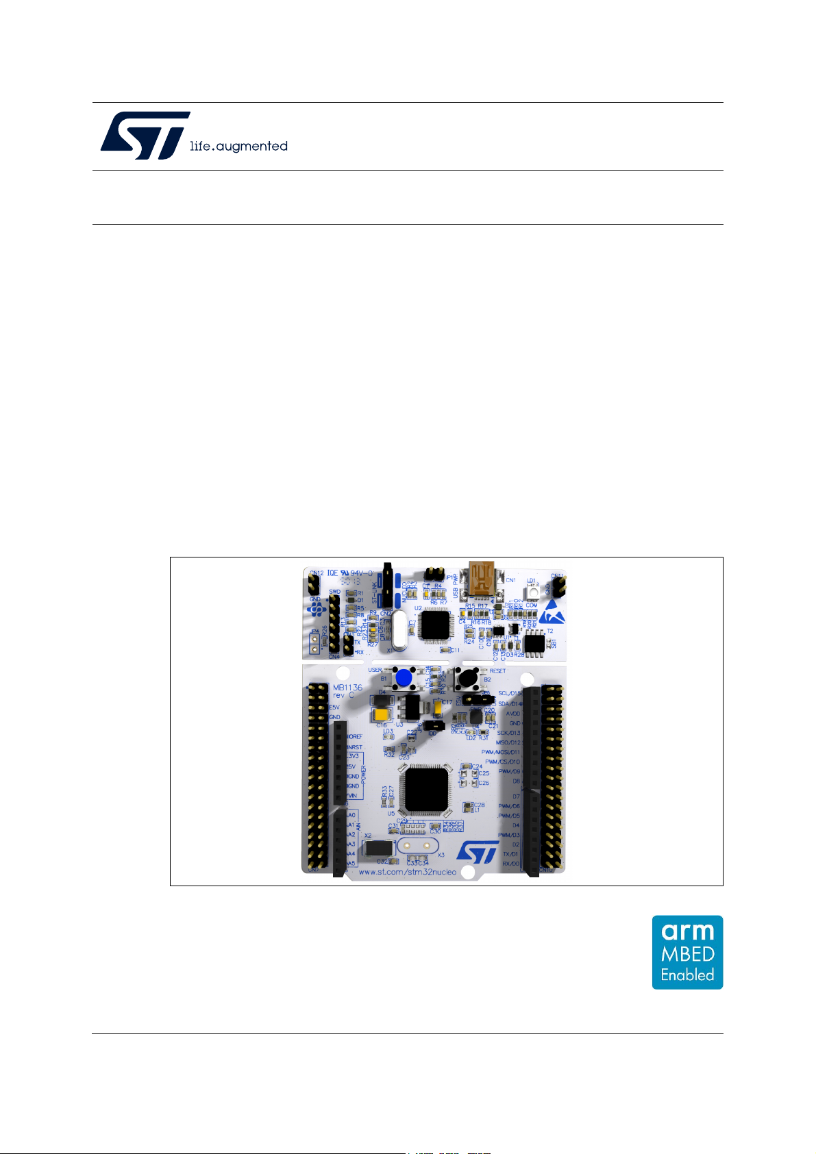
STM32 Nucleo-64 boards (MB1136) Introduction
The STM32 Nucleo-64 boards based on the MB1136 reference board (NUCLEO-F030R8,
NUCLEO-F070RB, NUCLEO-F072RB, NUCLEO-F091RC, NUCLEO-F103RB,
NUCLEO-F302R8, NUCLEO-F303RE, NUCLEO-F334R8, NUCLEO-F401RE,
NUCLEO-F410RB, NUCLEO-F411RE, NUCLEO-F446RE, NUCLEO-L010RB,
NUCLEO-L053R8, NUCLEO-L073RZ, NUCLEO-L152RE, NUCLEO-L452RE,
NUCLEO-L476RG) provide an affordable and flexible way for users to try out new concepts
and build prototypes with the STM32 microcontrollers in the LQFP64 package, choosing
from the various combinations of performance, power consumption, and features. The
ARDUINO® Uno V3 connectivity support and the ST morpho headers provide an easy
means of expanding the functionality of the Nucleo open development platform with a wide
choice of specialized shields. The STM32 Nucleo boards do not require any separate probe
as they integrate the ST-LINK/V2-1 debugger and programmer. The STM32 Nucleo boards
come with the comprehensive free software libraries and examples available with the
STM32Cube MCU Packages, as well as direct access to the Arm® Mbed™ online resources at http://mbed.org/.
Figure 1. STM32 Nucleo-64 board Picture is not contractual. August 2020 UM1724 Rev 14 1/68 www.st.com 1 Content UM1724 Content 1
Features . . . . . . . . . . . . . . . . . . . . . . . . . . . . . . . . . . . . . . . . . . . . . . . . . . . 6 2
Ordering information . . . . . . . . . . . . . . . . . . . . . . . . . . . . . . . . . . . . . . . . 7 2.1
Codification . . . . . . . . . . . . . . . . . . . . . . . . . . . . . . . . . . . . . . . . . . . . . . . . . 8 3
Development environment . . . . . . . . . . . . . . . . . . . . . . . . . . . . . . . . . . . . 9 3.1
System requirements . . . . . . . . . . . . . . . . . . . . . . . . . . . . . . . . . . . . . . . . . 9 3.2
Development toolchains . . . . . . . . . . . . . . . . . . . . . . . . . . . . . . . . . . . . . . . 9 3.3
Demonstration software . . . . . . . . . . . . . . . . . . . . . . . . . . . . . . . . . . . . . . . 9 4
Conventions . . . . . . . . . . . . . . . . . . . . . . . . . . . . . . . . . . . . . . . . . . . . . . . 9 5
Quick start . . . . . . . . . . . . . . . . . . . . . . . . . . . . . . . . . . . . . . . . . . . . . . . . 10 5.1
Getting started . . . . . . . . . . . . . . . . . . . . . . . . . . . . . . . . . . . . . . . . . . . . . 10 5.2
NUCLEO-L476RG bootloader limitations . . . . . . . . . . . . . . . . . . . . . . . . . 10 5.3
Hardware configuration variants . . . . . . . . . . . . . . . . . . . . . . . . . . . . . . . . .11 6
Hardware layout and configuration . . . . . . . . . . . . . . . . . . . . . . . . . . . . 12 6.1
Pre-cut PCB . . . . . . . . . . . . . . . . . . . . . . . . . . . . . . . . . . . . . . . . . . . . . . . 16 6.2
Embedded ST-LINK/V2-1 . . . . . . . . . . . . . . . . . . . . . . . . . . . . . . . . . . . . . 16 6.2.1
Driver . . . . . . . . . . . . . . . . . . . . . . . . . . . . . . . . . . . . . . . . . . . . . . . . . . 17 6.2.2
ST-LINK/V2-1 firmware upgrade . . . . . . . . . . . . . . . . . . . . . . . . . . . . . . 17 6.2.3
Using the ST-LINK/V2-1 to program and debug the STM32 on board . 18 6.2.4
Using ST-LINK/V2-1 to program and debug an external
STM32 application . . . . . . . . . . . . . . . . . . . . . . . . . . . . . . . . . . . . . . . . . 18 6.3
Power supply and power selection . . . . . . . . . . . . . . . . . . . . . . . . . . . . . . 20 6.3.1
Power supply input from the USB connector . . . . . . . . . . . . . . . . . . . . . 20 6.3.2
External power supply inputs: VIN and E5V . . . . . . . . . . . . . . . . . . . . . 21 6.3.3
External power supply input: +3.3V . . . . . . . . . . . . . . . . . . . . . . . . . . . . 22 6.3.4
External power supply output . . . . . . . . . . . . . . . . . . . . . . . . . . . . . . . . 22 6.4
LEDs . . . . . . . . . . . . . . . . . . . . . . . . . . . . . . . . . . . . . . . . . . . . . . . . . . . . 23 6.5
Push-buttons . . . . . . . . . . . . . . . . . . . . . . . . . . . . . . . . . . . . . . . . . . . . . . 23 6.6
JP6 (IDD) . . . . . . . . . . . . . . . . . . . . . . . . . . . . . . . . . . . . . . . . . . . . . . . . . 23 2/68 UM1724 Rev 14 UM1724 Content 6.7
OSC clock . . . . . . . . . . . . . . . . . . . . . . . . . . . . . . . . . . . . . . . . . . . . . . . . 24 6.7.1
OSC clock supply . . . . . . . . . . . . . . . . . . . . . . . . . . . . . . . . . . . . . . . . . 24 6.7.2
OSC 32 kHz clock supply . . . . . . . . . . . . . . . . . . . . . . . . . . . . . . . . . . . 25 6.8
USART communication . . . . . . . . . . . . . . . . . . . . . . . . . . . . . . . . . . . . . . 25 6.9
Solder bridges . . . . . . . . . . . . . . . . . . . . . . . . . . . . . . . . . . . . . . . . . . . . . 26 6.10
Extension connectors . . . . . . . . . . . . . . . . . . . . . . . . . . . . . . . . . . . . . . . . 27 6.11
ARDUINO® connectors . . . . . . . . . . . . . . . . . . . . . . . . . . . . . . . . . . . . . . 37 6.12
ST morpho connector . . . . . . . . . . . . . . . . . . . . . . . . . . . . . . . . . . . . . . . . 53 7
Nucleo-64 boards information . . . . . . . . . . . . . . . . . . . . . . . . . . . . . . . . 63 7.1
Product marking . . . . . . . . . . . . . . . . . . . . . . . . . . . . . . . . . . . . . . . . . . . . 63 7.2
Board revision history . . . . . . . . . . . . . . . . . . . . . . . . . . . . . . . . . . . . . . . . 64 7.3
Board known limitations . . . . . . . . . . . . . . . . . . . . . . . . . . . . . . . . . . . . . . 64
Revision history . . . . . . . . . . . . . . . . . . . . . . . . . . . . . . . . . . . . . . . . . . . . . . . . . . . . 65 UM1724 Rev 14 3/68 3 List of Tables UM1724 List of Tables Table 1.
Ordering information . . . . . . . . . . . . . . . . . . . . . . . . . . . . . . . . . . . . . . . . . . . . . . . . . . . . . . . 7 Table 2.
Codification explanation . . . . . . . . . . . . . . . . . . . . . . . . . . . . . . . . . . . . . . . . . . . . . . . . . . . . 8 Table 3.
ON/OFF conventions . . . . . . . . . . . . . . . . . . . . . . . . . . . . . . . . . . . . . . . . . . . . . . . . . . . . . . 9 Table 4.
Jumper states . . . . . . . . . . . . . . . . . . . . . . . . . . . . . . . . . . . . . . . . . . . . . . . . . . . . . . . . . . . 16 Table 5.
Debug connector CN4 (SWD) . . . . . . . . . . . . . . . . . . . . . . . . . . . . . . . . . . . . . . . . . . . . . . 19 Table 6.
JP1 configuration table . . . . . . . . . . . . . . . . . . . . . . . . . . . . . . . . . . . . . . . . . . . . . . . . . . . . 20 Table 7.
External power sources . . . . . . . . . . . . . . . . . . . . . . . . . . . . . . . . . . . . . . . . . . . . . . . . . . . 21 Table 8.
Power-related jumper . . . . . . . . . . . . . . . . . . . . . . . . . . . . . . . . . . . . . . . . . . . . . . . . . . . . . 21 Table 9.
+3.3 V external power source . . . . . . . . . . . . . . . . . . . . . . . . . . . . . . . . . . . . . . . . . . . . . . . 22 Table 10.
Solder bridges. . . . . . . . . . . . . . . . . . . . . . . . . . . . . . . . . . . . . . . . . . . . . . . . . . . . . . . . . . . 26 Table 11.
ARDUINO® connectors on NUCLEO-F030R8, NUCLEO-F070RB,
NUCLEO-F072RB, NUCLEO-F091RC . . . . . . . . . . . . . . . . . . . . . . . . . . . . . . . . . . . . . . . . 37 Table 12.
ARDUINO® connectors on NUCLEO-F103RB . . . . . . . . . . . . . . . . . . . . . . . . . . . . . . . . . . 39 Table 13.
ARDUINO® connectors on NUCLEO-F302R8 . . . . . . . . . . . . . . . . . . . . . . . . . . . . . . . . . . 40 Table 14.
ARDUINO® connectors on NUCLEO-F303RE . . . . . . . . . . . . . . . . . . . . . . . . . . . . . . . . . . 41 Table 15.
ARDUINO® connectors on NUCLEO-F334R8 . . . . . . . . . . . . . . . . . . . . . . . . . . . . . . . . . . 42 Table 16.
ARDUINO® connectors on NUCLEO-F401RE and NUCLEO-F411RE . . . . . . . . . . . . . . . 43 Table 17.
ARDUINO® connectors on NUCLEO-L053R8 . . . . . . . . . . . . . . . . . . . . . . . . . . . . . . . . . . 45 Table 18.
ARDUINO® connectors on NUCLEO-L010RB and NUCLEO-L073RZ . . . . . . . . . . . . . . . 46 Table 19.
ARDUINO® connectors on NUCLEO-F446RE . . . . . . . . . . . . . . . . . . . . . . . . . . . . . . . . . . 47 Table 20.
ARDUINO® connectors on NUCLEO-F410RB . . . . . . . . . . . . . . . . . . . . . . . . . . . . . . . . . . 49 Table 21.
ARDUINO® connectors on NUCLEO-L152RE . . . . . . . . . . . . . . . . . . . . . . . . . . . . . . . . . . 50 Table 22.
ARDUINO® connectors on NUCLEO-L452RE . . . . . . . . . . . . . . . . . . . . . . . . . . . . . . . . . . 51 Table 23.
ARDUINO® connectors on NUCLEO-L476RG . . . . . . . . . . . . . . . . . . . . . . . . . . . . . . . . . . 52 Table 24.
ST morpho connector on NUCLEO-F030R8 . . . . . . . . . . . . . . . . . . . . . . . . . . . . . . . . . . . 53 Table 25.
ST morpho connector on NUCLEO-F070RB . . . . . . . . . . . . . . . . . . . . . . . . . . . . . . . . . . . 54 Table 26. ST morpho connector on
NUCLEO-F072RB, NUCLEO-F091RC, NUCLEO-F303RE, NUCLEO-F334R8. . . . . . . . . 55 Table 27.
ST morpho connector on NUCLEO-F103RB . . . . . . . . . . . . . . . . . . . . . . . . . . . . . . . . . . . 55 Table 28.
ST morpho connector on NUCLEO-F302R8 . . . . . . . . . . . . . . . . . . . . . . . . . . . . . . . . . . . 57 Table 29.
ST morpho connector on NUCLEO-F401RE,
NUCLEO-F411RE, NUCLEO-F446RE . . . . . . . . . . . . . . . . . . . . . . . . . . . . . . . . . . . . . . . . 58 Table 30.
ST morpho connector on NUCLEO-L010RB,
NUCLEO-L053R8, NUCLEO-L073RZ, NUCLEO-L152RE . . . . . . . . . . . . . . . . . . . . . . . . . 59 Table 31.
ST morpho connector on NUCLEO-L452RE . . . . . . . . . . . . . . . . . . . . . . . . . . . . . . . . . . . 60 Table 32.
ST morpho connector on NUCLEO-L476RG . . . . . . . . . . . . . . . . . . . . . . . . . . . . . . . . . . . 61 Table 33.
ST morpho connector on NUCLEO-F410RB . . . . . . . . . . . . . . . . . . . . . . . . . . . . . . . . . . . 62 Table 34.
Document revision history . . . . . . . . . . . . . . . . . . . . . . . . . . . . . . . . . . . . . . . . . . . . . . . . . 65 4/68 UM1724 Rev 14 UM1724 List of Figures List of Figures Figure 1.
STM32 Nucleo-64 board. . . . . . . . . . . . . . . . . . . . . . . . . . . . . . . . . . . . . . . . . . . . . . . . . . . . 1 Figure 2.
Hardware block diagram . . . . . . . . . . . . . . . . . . . . . . . . . . . . . . . . . . . . . . . . . . . . . . . . . . 12 Figure 3.
Top layout . . . . . . . . . . . . . . . . . . . . . . . . . . . . . . . . . . . . . . . . . . . . . . . . . . . . . . . . . . . . . . 13 Figure 4.
Bottom layout . . . . . . . . . . . . . . . . . . . . . . . . . . . . . . . . . . . . . . . . . . . . . . . . . . . . . . . . . . . 14 Figure 5.
STM32 Nucleo board mechanical dimensions . . . . . . . . . . . . . . . . . . . . . . . . . . . . . . . . . . 15 Figure 6.
Typical configuration. . . . . . . . . . . . . . . . . . . . . . . . . . . . . . . . . . . . . . . . . . . . . . . . . . . . . . 17 Figure 7.
Updating the list of drivers in Device Manager . . . . . . . . . . . . . . . . . . . . . . . . . . . . . . . . . . 17 Figure 8.
Connecting the STM32 Nucleo board to program the on-board STM32 . . . . . . . . . . . . . . 18 Figure 9.
Using ST-LINK/V2-1 to program the STM32 on an external application . . . . . . . . . . . . . . 19 Figure 10.
NUCLEO-F030R8 . . . . . . . . . . . . . . . . . . . . . . . . . . . . . . . . . . . . . . . . . . . . . . . . . . . . . . . . 28 Figure 11.
NUCLEO-F070RB . . . . . . . . . . . . . . . . . . . . . . . . . . . . . . . . . . . . . . . . . . . . . . . . . . . . . . . 28 Figure 12.
NUCLEO-F072RB . . . . . . . . . . . . . . . . . . . . . . . . . . . . . . . . . . . . . . . . . . . . . . . . . . . . . . . 29 Figure 13.
NUCLEO-F091RC . . . . . . . . . . . . . . . . . . . . . . . . . . . . . . . . . . . . . . . . . . . . . . . . . . . . . . . 29 Figure 14.
NUCLEO-F103RB . . . . . . . . . . . . . . . . . . . . . . . . . . . . . . . . . . . . . . . . . . . . . . . . . . . . . . . 30 Figure 15.
NUCLEO-F302R8 . . . . . . . . . . . . . . . . . . . . . . . . . . . . . . . . . . . . . . . . . . . . . . . . . . . . . . . . 30 Figure 16.
NUCLEO-F303RE . . . . . . . . . . . . . . . . . . . . . . . . . . . . . . . . . . . . . . . . . . . . . . . . . . . . . . . 31 Figure 17.
NUCLEO-F334R8 . . . . . . . . . . . . . . . . . . . . . . . . . . . . . . . . . . . . . . . . . . . . . . . . . . . . . . . . 31 Figure 18.
NUCLEO-F401RE . . . . . . . . . . . . . . . . . . . . . . . . . . . . . . . . . . . . . . . . . . . . . . . . . . . . . . . 32 Figure 19.
NUCLEO-F411RE . . . . . . . . . . . . . . . . . . . . . . . . . . . . . . . . . . . . . . . . . . . . . . . . . . . . . . . 32 Figure 20.
NUCLEO-L053R8 . . . . . . . . . . . . . . . . . . . . . . . . . . . . . . . . . . . . . . . . . . . . . . . . . . . . . . . . 33 Figure 21.
NUCLEO-L073RZ and NUCLEO-L010RB . . . . . . . . . . . . . . . . . . . . . . . . . . . . . . . . . . . . . 33 Figure 22.
NUCLEO-L152RE. . . . . . . . . . . . . . . . . . . . . . . . . . . . . . . . . . . . . . . . . . . . . . . . . . . . . . . . 34 Figure 23.
NUCLEO-L452RE. . . . . . . . . . . . . . . . . . . . . . . . . . . . . . . . . . . . . . . . . . . . . . . . . . . . . . . . 34 Figure 24.
NUCLEO-L476RG . . . . . . . . . . . . . . . . . . . . . . . . . . . . . . . . . . . . . . . . . . . . . . . . . . . . . . . 35 Figure 25.
NUCLEO-F446RE . . . . . . . . . . . . . . . . . . . . . . . . . . . . . . . . . . . . . . . . . . . . . . . . . . . . . . . 35 Figure 26.
NUCLEO-F410RB . . . . . . . . . . . . . . . . . . . . . . . . . . . . . . . . . . . . . . . . . . . . . . . . . . . . . . . 36 UM1724 Rev 14 5/68 5 Features UM1724 1 Features
The STM32 Nucleo board offers the following features:
• STM32 microcontroller in LQFP64 package • Three LEDs:
– USB communication (LD1), user LED (LD2), power LED (LD3)
• Two push-buttons: USER and RESET
• Two types of extension resources
– ARDUINO® Uno V3 connectivity
– ST morpho extension pin headers for full access to all STM32 I/Os
• Flexible board power supply: –
USB VBUS or external source (3.3 V, 5 V, 7-12 V) – Power management access point
• On-board ST-LINK/V2-1 debugger and programmer with SWD connector
– Selection-mode switch using the kit as a standalone ST-LINK/V2-1
• USB re-enumeration capability. Three different interfaces supported on USB: – Virtual COM port – Mass storage – Debug port
• Comprehensive free software libraries and examples available with the STM32Cube MCU Package
• Arm® Mbed™(a) (see http://mbed.org)
a. Arm and Mbed are registered trademarks or trademarks of Arm Limited (or its subsidiaries) in the US and/or elsewhere. 6/68 UM1724 Rev 14 UM1724 Ordering information 2 Ordering information
To order an STM32 Nucleo-64 board, refer to Table 1. Additional information is available
from the datasheet and reference manual of the target STM32.
Table 1. Ordering information Board Order code Targeted STM32 Differentiating feature reference NUCLEO-F030R8 STM32F030R8T6 NUCLEO-F070RB STM32F070RBT6 NUCLEO-F072RB STM32F072RBT6 NUCLEO-F091RC STM32F091RCT6U NUCLEO-F103RB STM32F103RBT6 NUCLEO-F302R8 STM32F302R8T6 Arm® Mbed Enabled™ NUCLEO-F303RE STM32F303RET6 NUCLEO-F334R8 STM32F334R8T6 NUCLEO-F401RE STM32F401RET6U MB1136 NUCLEO-F410RB STM32F410RBT6U NUCLEO-F411RE STM32F411RET6U NUCLEO-F446RE STM32F446RET6U NUCLEO-L010RB STM32L010RBT6 - NUCLEO-L053R8 STM32L053R8T6 NUCLEO-L073RZ STM32L073RZT6U Arm® Mbed Enabled™ NUCLEO-L152RE STM32L152RET6 NUCLEO-L452RE STM32L452RET6U - NUCLEO-L476RG STM32L476RGT6U Arm® Mbed Enabled™ UM1724 Rev 14 7/68 67 Ordering information UM1724 2.1 Codification
The meaning of the codification is explained in Table 2.
Table 2. Codification explanation NUCLEO-XXYYRT Description Example: NUCLEO-L452RE MCU series in STM32 Arm XX STM32L4 Series Cortex MCUs STM32 product line in the YY STM32L452 series R STM32 package pin count 64 pins STM32 Flash memory size: – 8 for 64 Kbytes – B for 128 Kbytes T – C for 256 Kbytes 512 Kbytes – E for 512 Kbytes – G for 1 Mbyte – Z for 192 Kbytes
The order code is printed on a sticker placed at the top or bottom side of the board. 8/68 UM1724 Rev 14 UM1724 Development environment 3 Development environment 3.1 System requirements •
Windows® OS (7, 8 and 10), Linux® 64-bit, or macOS® • USB Type-A to Mini-B cable 3.2 Development toolchains •
IAR Systems - IAR Embedded Workbench®(a) • Keil®: MDK-ARM(a) • GCC-based IDEs •
Arm® Mbed™ online(b) (see http://mbed.org) 3.3 Demonstration software
The demonstration software, included in the STM32Cube MCU Package corresponding to
the on-board microcontroller, is preloaded in the STM32 Flash memory for easy
demonstration of the device peripherals in standalone mode. The latest versions of the
demonstration source code and associated documentation can be downloaded from www.st.com. 4 Conventions
Table 3 provides the conventions used for the ON and OFF settings in the present document.
Table 3. ON/OFF conventions Convention Definition Jumper JP1 ON Jumper fitted Jumper JP1 OFF Jumper not fitted Solder bridge SBx ON
SBx connections closed by solder or 0-ohm resistor Solder bridge SBx OFF SBx connections left open
In this document, the references are “STM32 Nucleo board” and “STM32 Nucleo boards” for
all information that is common to all sale types. a. On Windows® only.
b. Refer to the http://mbed.com website and to Table 1: Ordering information, to determine which order codes are supported. UM1724 Rev 14 9/68 67 Quick start UM1724 5 Quick start
The STM32 Nucleo board is a low-cost and easy-to-use development platform used to
quickly evaluate and start development with an STM32 microcontroller in LQFP64 package.
Before installing and using the product, accept the Evaluation Product License Agreement
from the www.st.com/epla web page.
For more information on the STM32 Nucleo board and to access the demonstration
software, visit www.st.com/stm32nucleo website. 5.1 Getting started
Follow the sequence below to configure the STM32 Nucleo board and launch the demo software: 1.
Check the jumper position on the board, JP1 off, JP5 (PWR) on U5V, JP6 on (IDD), CN2 on (NUCLEO) selected.
2. For correct identification of all device interfaces from the host PC, install the Nucleo
USB driver available from the www.st.com/stm32nucleo web page, prior to connecting the board.
3. Connect the STM32 Nucleo board to a PC with a USB cable ‘Type-A to Mini-B’ through
USB connector CN1 to power the board. The red LED LD3 (PWR) and LD1 (COM)
must light up. LD1 (COM) and green LED LD2 must blink.
4. Press button B1 (left button).
5. Observe the blinking frequency of LED LD2 at different frequencies, by clicking on the button B1.
6. The demonstration software and several software examples on how to use the STM32
Nucleo board features are available at the www.st.com/stm32nucleo web page.
7. Develop the application using the available examples. 5.2 NUCLEO-L476RG bootloader limitations
Boot from system Flash memory results in executing bootloader code stored in the system
Flash memory, protected against write and erase. This allows in-system programming (ISP),
that is, flashing the STM32 user Flash memory. It also allows writing data into RAM. The
data come in via one of the communication interfaces such as USART, SPI, I2C bus, USB, or CAN.
The bootloader version can be identified by reading the bootloader ID at the address 0x1FFF6FFE.
The STM32L476RGT6 part soldered on the NUCLEO-L476RG main board is marked with a
date code, corresponding to its date of manufacturing. STM32L476RGT6 parts with the date
code prior or equal to week 22 of 2015 are fitted with bootloader V 9.0, affected by the
limitations to be worked around, as described hereunder. Parts with the date code starting
from week 23 of 2015 contain bootloader V 9.2 in which the limitations no longer exist.
To locate the visual date code information on the STM32L476RGT6 package, refer to the
section “Package information” of the datasheet (DS10198) available at www.st.com. Date
code related portion of the package marking takes Y WW format, where Y is the last digit of 10/68 UM1724 Rev 14 UM1724 Quick start
the year and WW is the week. For example, a part manufactured in week 23 of 2015 bares the date code 5 23.
The bootloader ID of the bootloader V 9.0 is 0x90.
The following limitations exist in the bootloader V 9.0: 1.
RAM data get corrupted when written via USART/SPI/I2C/USB interface Description:
Data write operation into RAM space via USART, SPI, I2C bus, or USB results in wrong or no data written. Workaround:
To correct the issue of the wrong write into RAM, download STSW-STM32158 bootloader
V 9.0 patch package from the www.st.com website and load ‘Bootloader V9.0 SRAM patch’
to the STM32, following the information in readme.txt file available in the package.
2. User Flash memory data get corrupted when written via CAN interface Description:
Data write operation into user Flash memory space via CAN interface results in wrong or no data written. Workaround:
To correct the issue of the wrong write into Flash memory, download the STSW-STM32158
bootloader V 0.9 patch package from the www.st.com website and load ‘Bootloader V9.0
CAN patch’ to the STM32, following the information in readme.txt file available in the package. 5.3 Hardware configuration variants
The board can be delivered with different configurations of the oscillator of the target
STM32. For all the details concerning high-speed configurations of the oscillator refer to
Section 6.7.1. For all the details concerning low-speed configurations of the oscillator refer to Section 6.7.2. UM1724 Rev 14 11/68 67
Hardware layout and configuration UM1724 6
Hardware layout and configuration
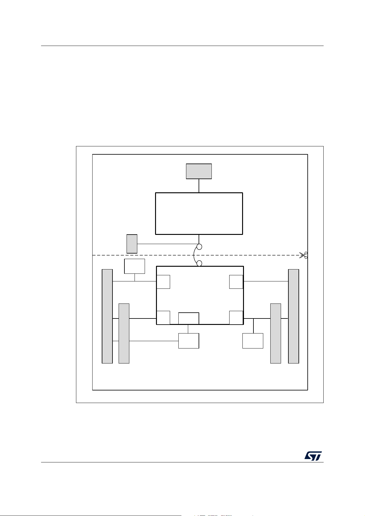
The STM32 Nucleo board is designed around the STM32 microcontrollers in a 64-pin LQFP package.
Figure 2 shows the connections between the STM32 and its peripherals (ST-LINK/V2-1,
push-button, LED, ARDUINO® connectors, and ST morpho connector).
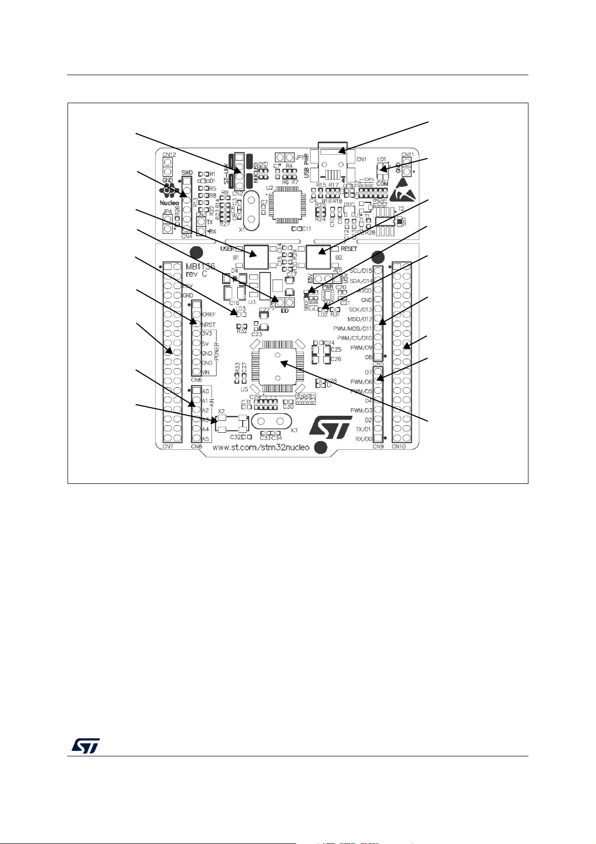
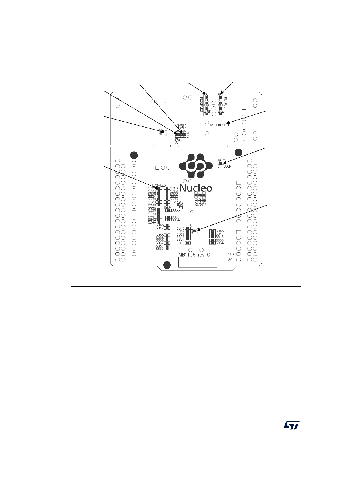
Figure 3 and Figure 4 show the location of these features on the STM32 Nucleo board.
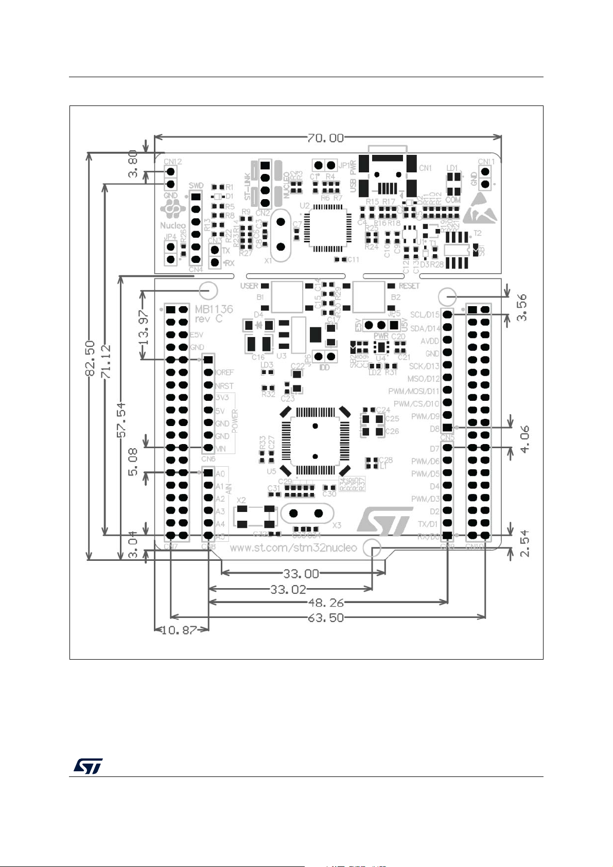
Figure 5 shows the mechanical dimension of the STM32 Nucleo board.
Figure 2. Hardware block diagram ST-LINK part Mini USB Embedded ST-LINK/V2-1 SWD B1 USER STM32 Microcontroller IO IO IO RESET IO connector connector ® ® morpho extension header B2 LED morpho extension header ST RESET LD4 ST ARDUINO ARDUINO MCU part MS34374V2 12/68 UM1724 Rev 14 UM1724
Hardware layout and configuration Figure 3. Top layout CN1 CN2 ST-LINK USB ST-LINK/Nucleo mini B connector selector LD1 (Red/Green LED) CN4 COM SWD connector B2 B1 USER RESET button button JP6 IDD SB2 measurement 3.3 V regulator outpu t LD3 LD2 (Red LED) (Green LED) power CN6 ARDUINO® CN5 connector ARDUINO® connector CN7 ST morpho CN10 connector ST morpho connector CN9 CN8 ARDUINO® connector ARDUINO® connector 32 KHz crystal(1) U5 STM32 microcontroller MS34376V3
1. Crystal may be present or not depending on board version, refer to Section 6.7.2. UM1724 Rev 14 13/68 67
Hardware layout and configuration UM1724 Figure 4. Bottom layout SB13, SB14 SB4, SB6, SB8, SB10 SB3, SB5, SB7, SB9 ST-LINK USART (RESERVED) (DEFAULT) SB15 ST-LINK SWO SB11 ST-LINK SB16 RESET ST-LINK MCO SB17 USER button SB21 USER LED SB50 ST-LINK MCO MS34375V1 14/68 UM1724 Rev 14 UM1724
Hardware layout and configuration
Figure 5. STM32 Nucleo board mechanical dimensions UM1724 Rev 14 15/68 67
Hardware layout and configuration UM1724 6.1 Pre-cut PCB
The STM32 Nucleo board is divided into two parts: ST-LINK part and target STM32 part.
The ST-LINK part of the PCB can be cut out to reduce the board size. In this case, the
remaining target STM32 part can only be powered by VIN, E5V, and +3.3V on the ST
morpho connector CN7, or VIN and +3.3V on ARDUINO® connector CN6. It is still possible
to use the ST-LINK part to program the main STM32 using wires between CN4 and SWD
signals available on the ST morpho connector (SWCLK CN7 pin 15 and SWDIO CN7 pin 13). 6.2 Embedded ST-LINK/V2-1
The ST-LINK/V2-1 programming and debugging tool is integrated into the STM32 Nucleo board.
The ST-LINK/V2-1 makes the STM32 Nucleo boards Mbed Enabled™.
The embedded ST-LINK/V2-1 supports only SWD for STM32 devices. For information about
debugging and programming features, refer to the user manual ST-LINK/V2 in-circuit
debugger/programmer for STM8 and STM32 (UM1075), which describes in details all the ST-LINK/V2 features.
The changes versus the ST-LINK/V2 version are listed below. •
New features supported on ST-LINK/V2-1: – USB software re-enumeration –
Virtual COM port interface on USB – Mass storage interface on USB –
USB power management request for more than 100 mA power on USB •
Features not supported on ST-LINK/V2-1: – SW IM interfa ce –
Minimum supported application voltage limited to 3 V • Known limitation: –
Activating the readout protection on ST-LINK/V2-1 target prevents the target
application from running afterward. The target readout protection must be kept
disabled on ST-LINK/V2-1 boards.
There are two different ways to use the embedded ST-LINK/V2-1 depending on the jumper
states (see Table 4 and Figure 6): •
Program/debug the on-board STM32 (Section 6.2.2) •
Program/debug an MCU in an external application board using a cable connected to
SWD connector CN4 (Section 6.2.4). Table 4. Jumper states Jumper state Description
ST-LINK/V2-1 functions enabled for on-board programming Both CN2 jumpers ON (default)
ST-LINK/V2-1 functions enabled for external CN4 connector Both CN2 jumpers OFF (SWD supported) 16/68 UM1724 Rev 14 UM1724
Hardware layout and configuration
Figure 6. Typical configuration Hardware requirements:
- Computer with Windows® 7, 8 or 10 - USB cable Type-A to Mini-B Development toolchain: - IAR™ EWARM - Keil® MDK-ARM - GCC-based IDE MS19052V5 6.2.1 Driver
Before connecting the Nucleo-64 board to a Windows 7, Windows 8, or Windows 10 PC via
USB, a driver for ST-LINK/V2-1 must be installed. It can be downloaded from the www.st.com website.
In case the STM32 Nucleo-64 board is connected to the PC before installing the driver, the
PC device manager may report some Nucleo interfaces as “Unknown”.
To recover from this situation, after installing the dedicated driver, the association of
“Unknown” USB devices found on the STM32 Nucleo-64 board to this dedicated driver,
must be updated in the device manager manually. Note:
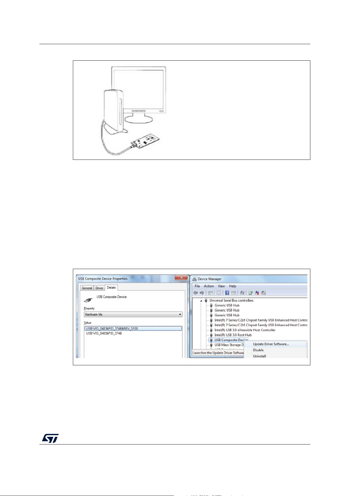
It is recommended to proceed using a USB Composite Device, as shown in Figure 7.
Figure 7. Updating the list of drivers in Device Manager 6.2.2
ST-LINK/V2-1 firmware upgrade
The ST-LINK/V2-1 embeds a firmware upgrade mechanism for the in-situ upgrade through
the USB port. As the firmware may evolve during the lifetime of the ST-LINK/V2-1 product
(for example new functionality, bug fixes, support for new microcontroller families), it is
recommended to visit www.st.com website before starting to use the STM32 Nucleo board
and periodically, in order to stay up-to-date with the latest firmware version. UM1724 Rev 14 17/68 67
Hardware layout and configuration UM1724 6.2.3
Using the ST-LINK/V2-1 to program and debug the STM32 on board
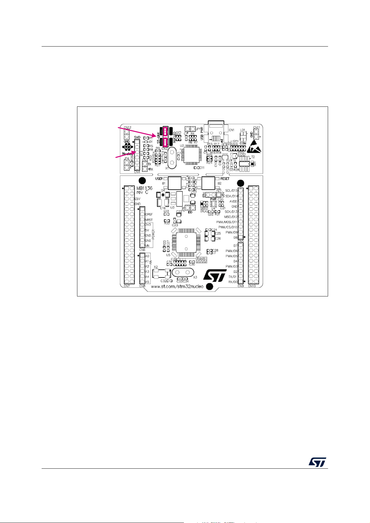
To program the STM32 on the board, plug in the two jumpers on CN2, as shown in red in
Figure 8. Do not use the CN4 connector as this could disturb the communication with the
STM32 microcontroller of the STM32 Nucleo board.
Figure 8. Connecting the STM32 Nucleo board to program the on-board STM32 CN2 jumpers ON CN4 SWD connector MS34378V2 6.2.4 Using ST-LINK/V2-1 to
program and debug an external STM32 application
It is very easy to use the ST-LINK/V2-1 to program the STM32 on an external application.
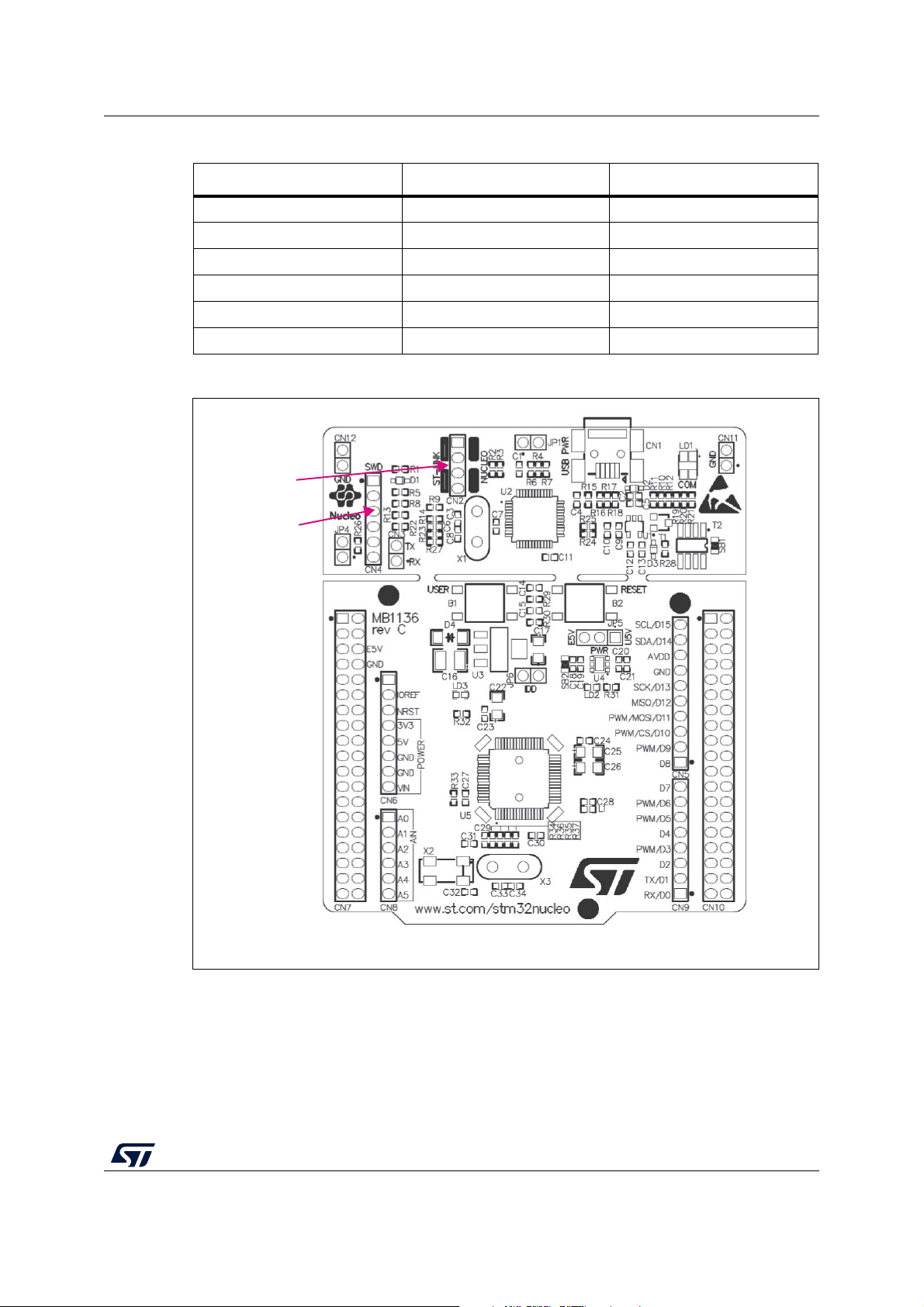
Simply remove the two jumpers from CN2 as illustrated in Figure 9: Using ST-LINK/V2-1 to
program the STM32 on an external application, and connect the application to the CN4
debug connector according to Table 5. Note:
SB12 NRST (target STM32 RESET) must be OFF if CN4 pin 5 is used in the external application. 18/68 UM1724 Rev 14 UM1724
Hardware layout and configuration
Table 5. Debug connector CN4 (SWD) Pin CN4 Designation 1 VDD_TARGET VDD from application 2 SWCLK SWD clock 3 GND ground 4 SWDIO SWD data input/output 5 NRST RESET of target STM32 6 SWO Reserved
Figure 9. Using ST-LINK/V2-1 to program the STM32 on an external application CN2 jumpers OFF CN4 SWD connector MS34379V2 UM1724 Rev 14 19/68 67
Hardware layout and configuration UM1724 6.3
Power supply and power selection
The power supply is provided either by the host PC through the USB cable, or by an
external source: VIN (From 7 V to 12 V), E5V (5 V) or +3.3V power supply pins on CN6 or
CN7. In case VIN, E5V or +3.3V is used to power the STM32 Nucleo board, using an
external power supply unit or auxiliary equipment, this power source must comply with the
standard EN-60950-1: 2006+A11/2009, and must be Safety Extra Low Voltage (SELV) with limited power capability. 6.3.1
Power supply input from the USB connector
The ST-LINK/V2-1 supports USB power management allowing to request more than 100 mA current to the host PC.
All parts of the STM32 Nucleo board and shield can be powered from the ST-LINK USB
connector CN1 (U5V or VBUS). Note that only the ST-LINK part is power supplied before
the USB enumeration as the host PC only provides 100 mA to the board at that time. During
the USB enumeration, the STM32 Nucleo board requires 300 mA of current to the host PC.
If the host is able to provide the required power, the targeted STM32 microcontroller is
powered and the red LED LD3 is turned ON, thus the STM32 Nucleo board and its shield
can consume a maximum of 300 mA current, not more. If the host is not able to provide the
required current, the targeted STM32 microcontroller and the MCU part including the
extension board are not power supplied. As a consequence, the red LED LD3 remains
turned OFF. In such a case it is mandatory to use an external power supply as explained in
the next Section 6.3.2: External power supply inputs: VIN and E5V.
When the board is power supplied by USB (U5V) a jumper must be connected between pin
1 and pin 2 of JP5 as shown in Table 8.
JP1 is configured according to the maximum current consumption of the board when
powered by USB (U5V). JP1 jumper can be set in case the board is powered by USB and
maximum current consumption on U5V does not exceed 100 mA (including an eventual
extension board or ARDUINO® shield). In such a condition, USB enumeration always
succeeds since no more than 100 mA is requested to the PC. Possible configurations of
JP1 are summarized in Table 6.
Table 6. JP1 configuration table Jumper state Power supply Allowed current JP1 jumper OFF 300 mA max USB power through CN1 JP1 jumper ON 100 mA max Warning:
If the maximum current consumption of the NUCLEO and its
extension boards exceeds 300 mA, it is mandatory to power
the NUCLEO using an external power supply connected to E5V or VIN. Note:
In case the board is powered by a USB charger, there is no USB enumeration, so the led
LD3 remains set to OFF permanently and the target STM32 is not powered. In this specific
case, the jumper JP1 needs to be set to ON, to allow target STM32 to be powered anyway. 20/68 UM1724 Rev 14