Power management techniques for integrated circuit design-Wiley (2016) | Tài liệu Tiếng Anh
Power management techniques for integrated circuit design Dành cho thiết kết Low Dropout Voltage Regulator . Tài liệu giúp bạn tham khảo, ôn tập và đạt kết quả cao. Mời đọc đón xem!
Môn: Tiếng Anh chuyên ngành 332 tài liệu
Trường: Tài liệu Tiếng Anh chuyên ngành, Tiếng Anh cho người đi làm 432 tài liệu
Tác giả:


Preview text:
POWER MANAGEMENT TECHNIQUES FOR INTEGRATED CIRCUIT DESIGN POWER MANAGEMENT TECHNIQUES FOR INTEGRATED CIRCUIT DESIGN Ke-Horng Chen
National Chiao Tung University, Taiwan
This edition first published 2016
© 2016 John Wiley & Sons Singapore Pte. Ltd. Registered Office
John Wiley & Sons Singapore Pte. Ltd., 1 Fusionopolis Walk, #07-01 Solaris South Tower, Singapore 138628.
For details of our global editorial offices, for customer services and for information about how to apply for permission
to reuse the copyright material in this book please see our website at www.wiley.com.
All Rights Reserved. No part of this publication may be reproduced, stored in a retrieval system or transmitted, in
any form or by any means, electronic, mechanical, photocopying, recording, scanning, or otherwise, except as expressly
permitted by law, without either the prior written permission of the Publisher, or authorization through payment of
the appropriate photocopy fee to the Copyright Clearance Center. Requests for permission should be addressed to the
Publisher, John Wiley & Sons Singapore Pte. Ltd., 1 Fusionopolis Walk, #07-01 Solaris South Tower, Singapore
138628, tel: 65-66438000, fax: 65-66438008, email: enquiry@wiley.com.
Wiley also publishes its books in a variety of electronic formats. Some content that appears in print may not be available in electronic books.
Designations used by companies to distinguish their products are often claimed as trademarks. All brand names
and product names used in this book are trade names, service marks, trademarks or registered trademarks of their
respective owners. The Publisher is not associated with any product or vendor mentioned in this book. This publication
is designed to provide accurate and authoritative information in regard to the subject matter covered. It is sold on
the understanding that the Publisher is not engaged in rendering professional services. If professional advice or
other expert assistance is required, the services of a competent professional should be sought.
Limit of Liability/Disclaimer of Warranty: While the publisher and author have used their best efforts in preparing
this book, they make no representations or warranties with respect to the accuracy or completeness of the contents
of this book and specifically disclaim any implied warranties of merchantability or fitness for a particular purpose.
It is sold on the understanding that the publisher is not engaged in rendering professional services and neither the
publisher nor the author shall be liable for damages arising herefrom. If professional advice or other expert
assistance is required, the services of a competent professional should be sought.
Library of Congress Cataloging-in-Publication Data Names: Chen, Ke-Horng, author.
Title: Power management techniques for integrated circuit design / Ke-Horng Chen.
Description: Chichester, UK ; Hoboken, NJ : John Wiley & Sons, 2016. |
Includes bibliographical references and index.
Identifiers: LCCN 2016002873 (print) | LCCN 2016007188 (ebook) | ISBN
9781118896815 (cloth) | ISBN 9781118896822 (pdf) | ISBN 9781118896839 (epub)
Subjects: LCSH: Voltage regulators—Design and construction. | Power
semiconductors–Design and construction. | Integrated circuits—Design and
construction. | Electric power—Conservation.
Classification: LCC TK2851 .C5138 2016 (print) | LCC TK2851 (ebook) | DDC 621.39/5—dc23
LC record available at http://lccn.loc.gov/2016002873
Cover image: Photoslash/iStockphoto
Set in 10 /12pt Times by SPi Global, Pondicherry, India 1 2016
To my respected parents, Li-Yun Wu and He-Nan Chen, and my wife, Hsin-Hua Pai Contents About the Author xii Preface xiii Acknowledgments xv 1 Introduction 1 1.1 Moore’s Law 1 1.2
Technology Process Impact: Power Management IC from 0.5 micro-meter to 28 nano-meter 1 1.2.1 MOSFET Structure 1 1.2.2 Scaling Effects 7 1.2.3
Leakage Power Dissipation 9 1.3
Challenge of Power Management IC in Advanced Technological Products 14 1.3.1 Multi-Vth Technology 14 1.3.2 Performance Boosters 15 1.3.3
Layout-Dependent Proximity Effects 19 1.3.4
Impacts on Circuit Design 20 1.4
Basic Definition Principles in Power Management Module 22 1.4.1 Load Regulation 22 1.4.2
Transient Voltage Variations 23 1.4.3
Conduction Loss and Switching Loss 24 1.4.4
Power Conversion Efficiency 25 References 25
2 Design of Low Dropout (LDO) Regulators 28 2.1 Basic LDO Architecture 29 2.1.1 Types of Pass Device 31 2.2 Compensation Skills 34 2.2.1 Pole Distribution 34 viii Contents 2.2.2
Zero Distribution and Right-Half-Plane (RHP) Zero 40 2.3
Design Consideration for LDO Regulators 42 2.3.1 Dropout Voltage 43 2.3.2 Efficiency 44 2.3.3 Line/Load Regulation 45 2.3.4
Transient Output Voltage Variation Caused by Sudden Load Current Change 46 2.4 Analog-LDO Regulators 50 2.4.1
Characteristics of Dominant-Pole Compensation 50 2.4.2
Characteristics of C-free Structure 56 2.4.3
Design of Low-Voltage C-free LDO Regulator 62 2.4.4
Alleviating Minimum Load Current Constraint through the Current
Feedback Compensation (CFC) Technique in the Multi-stage
C-free LDO Regulator 66 2.4.5
Multi-stage LDO Regulator with Feedforward Path and Dynamic Gain Adjustment (DGA) 75 2.5
Design Guidelines for LDO Regulators 79 2.5.1
Simulation Tips and Analyses 81 2.5.2
Technique for Breaking the Loop in AC Analysis Simulation 82 2.5.3
Example of the Simulation Results of the LDO Regulator with Dominant-Pole Compensation 85 2.6 Digital-LDO (D-LDO) Design 93 2.6.1 Basic D-LDO 94 2.6.2
D-LDO with Lattice Asynchronous Self-Timed Control 96 2.6.3
Dynamic Voltage Scaling (DVS) 100 2.7
Switchable Digital/Analog-LDO (D/A-LDO) Regulator with Analog DVS Technique 110 2.7.1 ADVS Technique 110 2.7.2
Switchable D/A-LDO Regulator 113 References 120
3 Design of Switching Power Regulators 122 3.1 Basic Concept 122 3.2
Overview of the Control Method and Operation Principle 125 3.3
Small Signal Modeling and Compensation Techniques in SWR 131 3.3.1
Small Signal Modeling of Voltage-Mode SWR 131 3.3.2
Small Signal Modeling of the Closed-Loop Voltage-Mode SWR 135 3.3.3
Small Signal Modeling of Current-Mode SWR 150 References 169
4 Ripple-Based Control Technique Part I 170 4.1
Basic Topology of Ripple-Based Control 171 4.1.1 Hysteretic Control 173 4.1.2 On-Time Control 176 Contents ix 4.1.3 Off-Time Control 179 4.1.4
Constant Frequency with Peak Voltage Control and Constant
Frequency with Valley Voltage Control 182 4.1.5
Summary of Topology of Ripple-Based Control 183 4.2
Stability Criterion of On-Time Controlled Buck Converter 185 4.2.1
Derivation of the Stability Criterion 185 4.2.2
Selection of Output Capacitor 197 4.3
Design Techniques When Using MLCC with a Small Value of RESR 201 4.3.1
Use of Additional Ramp Signal 202 4.3.2
Use of Additional Current Feedback Path 204 4.3.3
Comparison of On-Time Control with an Additional Current Feedback Path 254 4.3.4
Ripple-Reshaping Technique to Compensate a Small Value of RESR 256 4.3.5
Experimental Result of Ripple-Reshaped Function 262 References 269
5 Ripple-Based Control Technique Part II 270 5.1
Design Techniques for Enhancing Voltage Regulation Performance 270 5.1.1
Accuracy in DC Voltage Regulation 270 5.1.2
V2 Structure for Ripple-Based Control 271 5.1.3
V2 On-Time Control with an Additional Ramp or Current Feedback Path 275 5.1.4
Compensator for V2 Structure with Small RESR 277 5.1.5
Ripple-Based Control with Quadratic Differential and Integration
Technique if Small RESR is Used 283 5.1.6
Robust Ripple Regulator (R3) 294 5.2
Analysis of Switching Frequency Variation to Reduce Electromagnetic Interference 297 5.2.1
Improvement of Noise Immunity of Feedback Signal 298 5.2.2
Bypassing Path to Filter the High-Frequency Noise of the Feedback Signal 299 5.2.3
Technique of PLL Modulator 302 5.2.4
Full Analysis of Frequency Variation under Different vIN, vOUT, and iLoad 304 5.2.5
Adaptive On-Time Controller for Pseudo-Constant fSW 313 5.3
Optimum On-Time Controller for Pseudo-Constant fSW 321 5.3.1
Algorithm for Optimum On-Time Control 322 5.3.2
Type-I Optimum On-Time Controller with Equivalent VIN and VOUT,eq 323 5.3.3
Type-II Optimum On-Time Controller with Equivalent VDUTY 331 5.3.4 Frequency Clamper 333 5.3.5
Comparison of Different On-Time Controllers 333 5.3.6
Simulation Result of Optimum On-Time Controller 335 5.3.7
Experimental Result of Optimum On-Time Controller 335 References 343 x Contents
6 Single-Inductor Multiple-Output (SIMO) Converter 345 6.1
Basic Topology of SIMO Converters 345 6.1.1 Architecture 345 6.1.2 Cross Regulation 347 6.2
Applications of SIMO Converters 348 6.2.1 System-on-Chip 348 6.2.2
Portable Electronics Systems 350 6.3
Design Guidelines of SIMO Converters 351 6.3.1 Energy Delivery Paths 351 6.3.2
Classifications of Control Methods 359 6.3.3 Design Goals 363 6.4
SIMO Converter Techniques for Soc 364 6.4.1
Superposition Theorem in Inductor Current Control 364 6.4.2
Dual-Mode Energy Delivery Methodology 366 6.4.3 Energy-Mode Transition 367 6.4.4 Automatic Energy Bypass 371 6.4.5
Elimination of Transient Cross Regulation 372 6.4.6 Circuit Implementations 376 6.4.7 Experimental Results 387 6.5
SIMO Converter Techniques for Tablets 397 6.5.1
Output Independent Gate Drive Control in SIMO Converter 397 6.5.2
CCM/GM Relative Skip Energy Control in SIMO Converter 405 6.5.3
Bidirectional Dynamic Slope Compensation in SIMO Converter 415 6.5.4 Circuit Implementations 420 6.5.5 Experimental Results 427 References 441
7 Switching-Based Battery Charger 443 7.1 Introduction 443 7.1.1 Pure Charge State 447 7.1.2 Direct Supply State 448 7.1.3 Plug Off State 448 7.1.4 CAS State 448 7.2
Small Signal Analysis of Switching-Based Battery Charger 449 7.3 Closed-Loop Equivalent Model 454 7.4 Simulation with PSIM 461 7.5 Turbo-boost Charger 465 7.6
Influence of Built-In Resistance in the Charger System 470 7.7
Design Example: Continuous Built-In Resistance Detection 472 7.7.1 CBIRD Operation 473 7.7.2
CBIRD Circuit Implementation 476 7.7.3 Experimental Results 480 References 482 Contents xi
8 Energy-Harvesting Systems 483 8.1
Introduction to Energy-Harvesting Systems 483 8.2 Energy-Harvesting Sources 486 8.2.1
Vibration Electromagnetic Transducers 487 8.2.2 Piezoelectric Generator 490 8.2.3
Electrostatic Energy Generator 491 8.2.4
Wind-Powered Energy Generator 492 8.2.5
Thermoelectric Generator 494 8.2.6 Solar Cells 496 8.2.7 Magnetic Coil 498 8.2.8 RF/Wireless 501 8.3 Energy-Harvesting Circuits 502 8.3.1
Basic Concept of Energy-Harvesting Circuits 502 8.3.2
AC Source Energy-Harvesting Circuits 505 8.3.3
DC-Source Energy-Harvesting Circuits 511 8.4 Maximum Power Point Tracking 514 8.4.1
Basic Concept of Maximum Power Point Tracking 514 8.4.2 Impedance Matching 515 8.4.3 Resistor Emulation 516 8.4.4 MPPT Method 518 References 523 Index 527 About the Author
Ke-Horng Chen received his B.S., M.S., and Ph.D. degrees in electrical engineering from the
National Taiwan University, Taipei, Taiwan in 1994, 1996, and 2003, respectively.
From 1996 to 1998, he was a part-time IC Designer at Philips, Taipei, Taiwan. From 1998 to
2000, he was an Application Engineer at Avanti Ltd., Taiwan. From 2000 to 2003, he was a
Project Manager at ACARD Ltd., where he was engaged in designing power management ICs.
He is currently Director of the Institute of Electrical Control Engineering and a Professor with
the Department of Electrical and Computer Engineering, National Chiao Tung University,
Hsinchu, Taiwan, where he has organized a Mixed-Signal and Power Management IC Labora-
tory. He is the author or coauthor of more than 200 papers published in journals and confer-
ences, and also holds several patents. His current research interests include power management
ICs, mixed-signal circuit designs, and display algorithm and driver designs of liquid crystal display (LCD) TVs.
Dr. Chen has served as an Associate Editor of IEEE Transactions on Power Electronics and
IEEE Transactions on Circuits and Systems – Part II: Express Briefs. He is also an Associate
Editor of IEEE Transactions on Circuits and Systems – Part I. He joined the Editorial Board of
Analog Integrated Circuits and Signal Processing in 2013. He is on the IEEE Circuits and Sys-
tems (CAS) VLSI Systems and Applications Technical Committee, and the IEEE CAS Power
and Energy Circuits and Systems Technical Committee. He belongs to the Society for Infor-
mation Display (SID) and International Display Manufacturing Conference (IDMC) Technical
Program Sub-committees. He is Tutorial Co-Chair of IEEE Asia Pacific Conference on Circuits
and Systems (APCCAS) 2012 and Track Chair of Integrated Power Electronics, IEEE Inter-
national Conference on Power Electronics and Drive Systems (PEDS) 2013. He is Technical
Program Co-Chair of IEEE International Future Energy Electronics Conference (IFEEC) 2013.
He has served as CAS Taipei Section Chair since 2015. He is also Technical Program Com-
mittee Member, European Solid-State Circuits Conference (ESSCIRC) 2014–present. Preface
Over the past three decades, power management technology has become more important as
portable and wearable electronics have become part of our daily lives. It is important to realize
the detailed design of power management circuits, including low dropout (LDO) regulators,
switching power converters (SWRs), switched-capacitor designs among others, if battery usage
lifetime and power-conversion efficiency need to be extended. Although some circuits can be
found in analog or power electronics books, the reader cannot get an overall understanding of
power management designs. Thus, I have written this book to collect useful material related to
power management designs in recent years.
Power management IC designs use low-voltage (LV) and high-voltage (HV) devices. The
specialty of this book is including LV and HV power management designs. Moreover, the
objective of the book is to let the reader understand the process trend and demand of today’s
applications from the first. The mathematical analysis in the book is simplified, because in my
opinion the reader needs to have the ability to understand the function of power management
circuits. After that, the reader can analyze the whole power system and derive the complicated
mathematical results. Thus, I have used many easy-to-understand figures in the book to let the
reader realize why and how power management should be implemented. Although the reader
can understand this via derived equations in some similar books, they can have the fun of think-
ing about and implementing their own designs if they study the circuits in this book by inspec-
tion rather than by equations. Moreover, digital and analog design techniques are introduced
because a combination of digital and analog skills can give maximum performance of power
management in system-on-chip (SoC) applications.
I have taught most of the material in this book both at the National Chiao Tung University,
Hsinchu, Taiwan and in Taiwan industry. The order, the format, and the content are all carefully
polished when I deliver the material to readers. It is a pity that much material is not included in
this book. However, I encourage the reader to apply the concepts to similar power management
designs. I have included some design guidelines in this book to let the reader realize the object- ive of each design.
Chapter 1 provides the reader with knowledge of LV and HV device characteristics and
structure in different advanced technologies for learning the material in this book. xiv Preface
Chapter 2 describes the general design of an LDO regulator used in many power manage-
ment circuits. Compensation skills are introduced to let the reader realize how to ensure power
stability in case of any disturbance from input, output, and loading. A digital LDO regulator is
also included for LV applications.
Chapter 3 includes the design guidelines of voltage-mode and current-mode switching power
regulators. Compensation skills are also introduced to quantify the behavior of basic pulse-
width-modulation (PWM) SWRs by inspection.
Chapter 4 introduces the ripple-based control technique for some applications that demand
the features of fast transient response, low power consumption, and compact size solution. In
particular, fast transient response is the trend for SWR designs to improve the performance of
dynamic voltage/frequency scaling techniques and/or reference tracking techniques.
Chapter 5 shows some ripple-based control techniques to improve the performance of basic
designs. Even if parasitic effects become large, the techniques presented here can still have
excellent performance. Readers can train themselves by using the circuits in this book, proved
for silicon, to implement useful power management circuits.
Chapter 6 shows state-of-the-art single-inductor multiple-output (SIMO) converters used in
SoC to minimize the power module size. The power stage design and controller design are
included in this chapter. We use the design concepts introduced in Chapters 2–5. The reader
can obtain advanced training in power management designs here.
Chapter 7 shows the switching-based battery charger to complete the full function of power
management in SoC designs. The basic stability proved by some behavior simulators can let the
reader know how to model and increase the whole battery charger system.
Chapter 8 includes some energy-harvesting techniques to let the reader realize the possibility
of obtaining energy from the environment. How to convert and how to improve efficiency are shown in this chapter. Acknowledgments
This book has benefited from the recent research results of my Master and Ph.D. students.
Many experts in both this research field and industry contributed much useful material to this
book. Among them are Shen-Yu Peng (National Chiao Tung University, Hsinchu, Taiwan),
Meng-Wei Chien (RealTek Corporation, Hsinchu, Taiwan), and Ying-Wei Chou (MediaTek
Inc., Hsinchu, Taiwan). I say “thank you” to them.
I thank Yu-Huei Lee (RichTek Inc., Hsinchu, Taiwan), Yi-Ping Su (NovaTek Inc., Hsinchu,
Taiwan), Wei-Chung Chen (MediaTek Inc., Hsinchu, Taiwan), Te-Fu Yang (Phison Electron-
ics Corporation, Hsinchu, Taiwan), and Tzu-Chi Huang (MediaTek Inc., Hsinchu, Taiwan) for
their contributions to this book.
My wife, Hsin-Hua, has made some contributions to this book. She encouraged me to com-
plete the whole book using a range of useful circuits proved for silicon. She collected much
useful material, including simulation and experimental results.
The book’s production was made possible with the cooperation of staff at John Wiley.
I thank James Murphy, Preethi Belkese, Maggie Zhang, Gunalan Lakshmipathy, Revathy
Kaliyamoorthy, and Clarissa Lim. Without their help, there would be no book. 1 Introduction 1.1 Moore’s Law
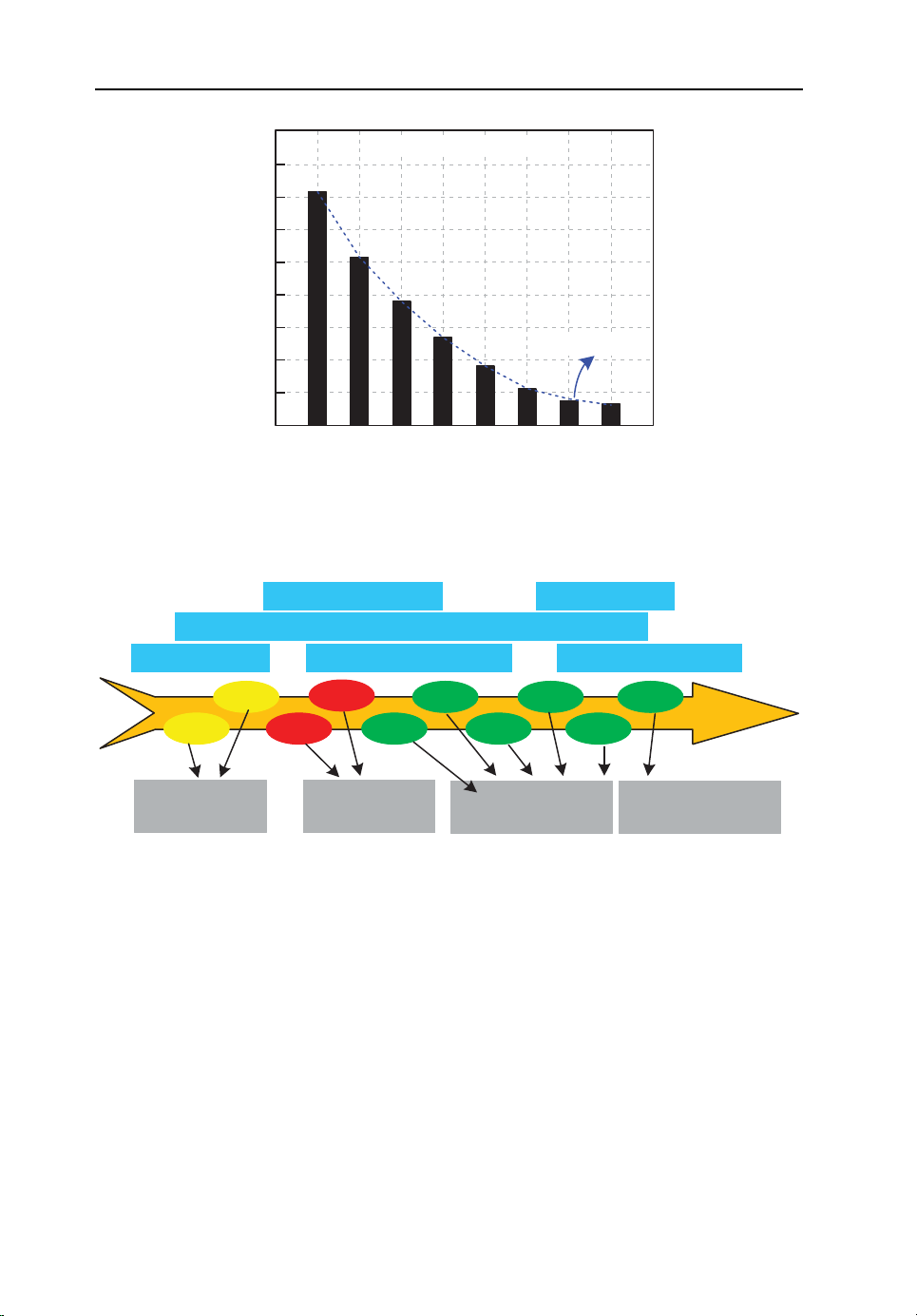
Over the past few decades, the number of transistors per square inch on integrated circuits (ICs)
has doubled every 18 months, which is the forecast of Moore’s law and is a continuing
condition. However, a physical limitation appears when the transistor size shrinks to 28 nm.
Several technology performance boosters, for example dual stress liner (DSL) technology,
strained silicon techniques, and the stress memorization technique (SMT), are required to retain
the performance of transistors. The industry has failed to keep to the trend predicted by Moore’s
law. Figure 1.1 depicts how the rate of transistor size scaling has slowed down and is likely to
break Moore’s law by the end of 2015.
1.2 Technology Process Impact: Power Management IC from
0.5 micro-meter to 28 nano-meter 1.2.1 MOSFET Structure
The voltage stress issue of metal–oxide–semiconductor field-effect transistors (MOSFETs) in
drivers and power MOSFETs needs careful consideration. The evolution of MOSFETs and their
applications are based on different input supply voltage (Figure 1.2). In advanced processes
(i.e., 40, 28, and 22 nm), core MOSFETs with characteristics of small silicon size and high speed
are used in low-voltage applications. Moreover, conventional low-voltage MOSFETs are
applied for low supply voltage conditions in normal processes, such as 22 nm, 0.18 μm,
0.25 μm, and 0.5 μm. Nevertheless, the drain-to-source voltage, VDS of low-voltage MOSFETs
cannot tolerate a high voltage and punches, and will break the MOSFET when the input supply
voltage increases. Therefore, double-diffused metal–oxide–semiconductors (DMOSs), vertical
Power Management Techniques for Integrated Circuit Design, First Edition. Ke-Horng Chen.
© 2016 John Wiley & Sons Singapore Pte Ltd. Published 2016 by John Wiley & Sons Singapore Pte Ltd. 2
Power Management Techniques for Integrated Circuit Design Industry transistor size (nm) 200 175 150 125 100 75 Slowing 50 25 0 2002 04 06 08 10 12 14 16 Year
Figure 1.1 Transistor size scaling rate has slowed down Home entertainment Power devices Medical devices Energy harvesting Mobile systems Consumer electronics Industrial applications 1.8 V 5 V 24 V 60 V >100 V 1.05 V 3.3 V 10 V 40 V 80 V Ultra-low Common Ultra-high High voltage voltage voltage voltage Core MOS Low-voltage MOS DMOS, LDMOS, and HVMOS
Figure 1.2 Evolution of MOSFETs and applications with different input supply voltages
double-diffused metal–oxide–semiconductors (VDMOSs), and laterally diffused metal–oxide–
semiconductors (LDMOSs) are applied to bear a high VDS. However, the gate-to-source voltage,
VGS of such MOSFETs cannot endure a high voltage, which will also damage the MOSFET.
A high-voltage metal–oxide–semiconductor (HVMOS) solves the problem here, because its
structure can tolerate a high voltage of both VDS and VGS.
The structures and characteristics of low-voltage MOSFETs, core MOSFETs, DMOSs,
VDMOSs, LDMOSs, and HVMOSs are introduced in the following subsections, followed
by a comparison of these MOSFETs.
Tài liệu liên quan:
-

Cambridge IELTS 13 Test-1 Overview and Practice Review | Tài liệu Tiếng Anh
6 3 -

IELTS Test 2 Review - Cambridge 13 Preparation Guide | Tài liệu Tiếng Anh
8 4 -

Litfocus Litreading Survey: Student Reading Interests & Habits Questionnaire | Tài liệu Tiếng Anh
7 4 -

Sách Pre-intermediate Market leader - Business English Course Book
23 12 -

Exam booster for B1 preliminary and B1 preliminary for schools with answer key
9 5