SLIDE Week 12 – Lecture 12 – Memory Kiến Trúc Máy Tính | Trường Đại học Công nghệ, Đại học Quốc gia Hà Nội
SLIDE Week 12 – Lecture 12 – Memory Kiến Trúc Máy Tính | Trường Đại học Công nghệ, Đại học Quốc gia Hà Nội . Tài liệu được sưu tầm và biên soạn dưới dạng PDF gồm 27 trang giúp bạn tham khảo, củng cố kiến thức và ôn tập đạt kết quả cao trong kỳ thi sắp tới. Mời bạn đọc đón xem!
Môn: Kiến Trúc Máy Tính (UET) 20 tài liệu
Trường: Trường Đại học Công nghệ, Đại học Quốc gia Hà Nội 824 tài liệu
Tác giả:
Preview text:
ELT3047 Computer Architecture Lecture 12: Memory Hoang Gia Hung
Faculty of Electronics and Telecommunications
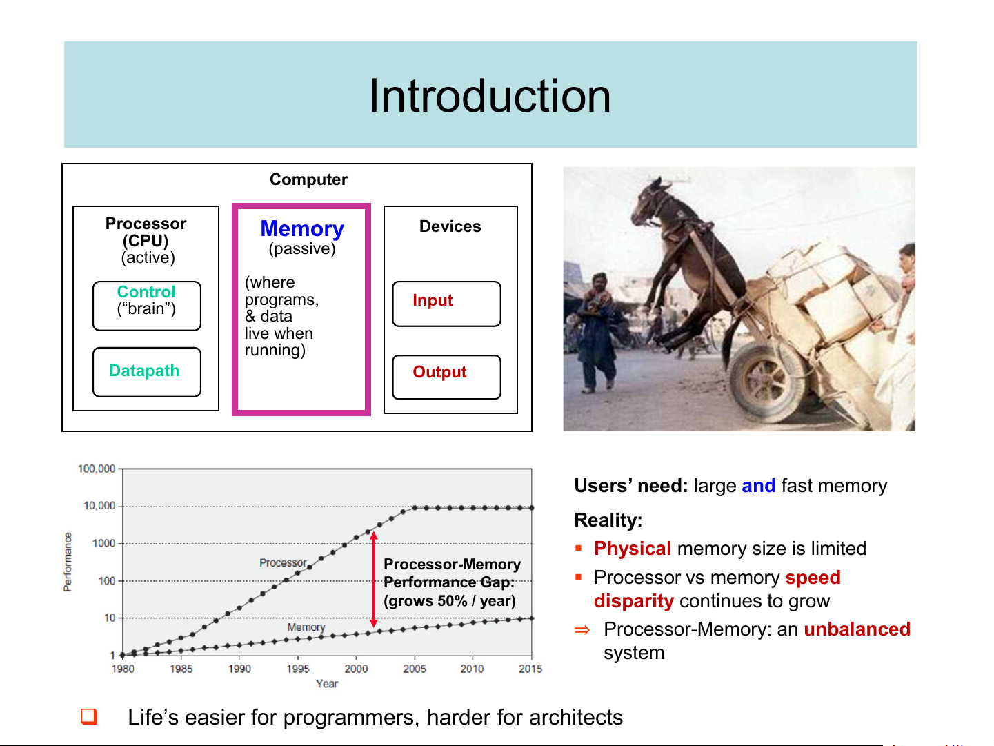
University of Engineering and Technology, VNU Hanoi Introduction Computer Processor Memory Devices (CPU) (passive) (active) (where Control (“brain”) programs, Input & data live when running) Datapath Output
Users’ need: large and fast memory Reality:
▪ Physical memory size is limited Processor-Memory Performance Gap:
▪ Processor vs memory speed (grows 50% / year)
disparity continues to grow
⇒ Processor-Memory: an unbalanced system ❑
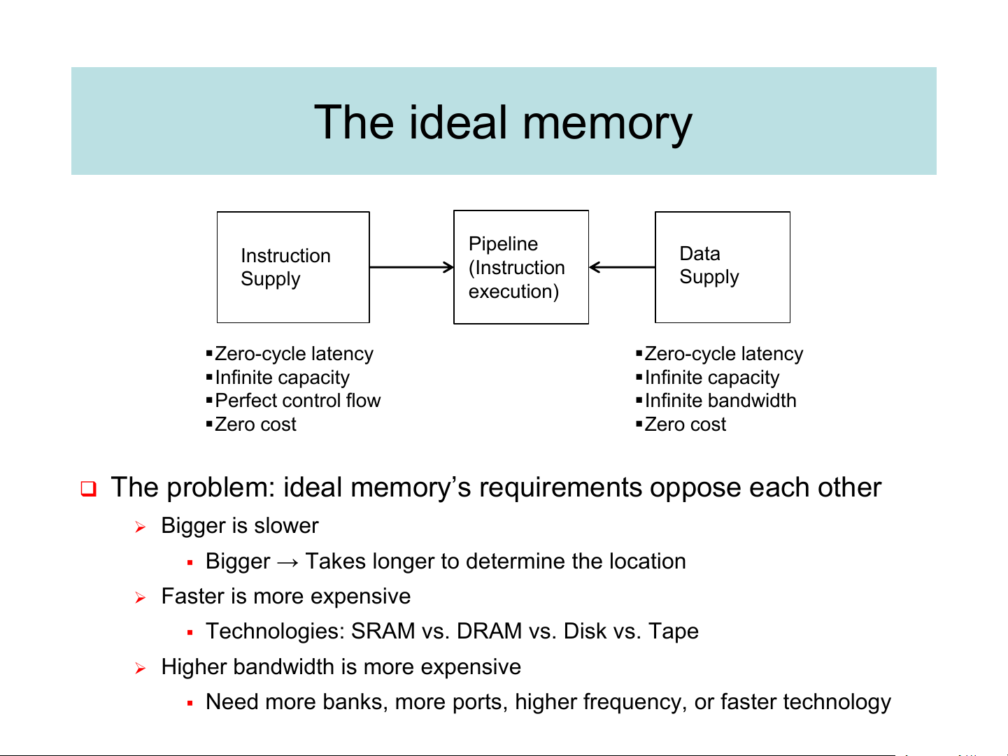
Life’s easier for programmers, harder for architects The ideal memory Pipeline Instruction Data (Instruction Supply Supply execution) ▪Zero-cycle latency ▪Zero-cycle latency ▪Infinite capacity ▪Infinite capacity ▪Perfect control flow ▪Infinite bandwidth ▪Zero cost ▪Zero cost
❑ The problem: ideal memory’s requirements oppose each other ➢ Bigger is slower
▪ Bigger → Takes longer to determine the location ➢ Faster is more expensive
▪ Technologies: SRAM vs. DRAM vs. Disk vs. Tape
➢ Higher bandwidth is more expensive
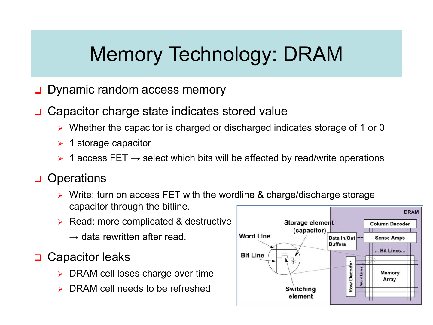
▪ Need more banks, more ports, higher frequency, or faster technology Memory Technology: DRAM
❑ Dynamic random access memory
❑ Capacitor charge state indicates stored value
➢ Whether the capacitor is charged or discharged indicates storage of 1 or 0 ➢ 1 storage capacitor
➢ 1 access FET → select which bits wil be affected by read/write operations ❑ Operations
➢ Write: turn on access FET with the wordline & charge/discharge storage capacitor through the bitline.
➢ Read: more complicated & destructive → data rewritten after read. ❑ Capacitor leaks
➢ DRAM cell loses charge over time
➢ DRAM cell needs to be refreshed Memory Technology: SRAM
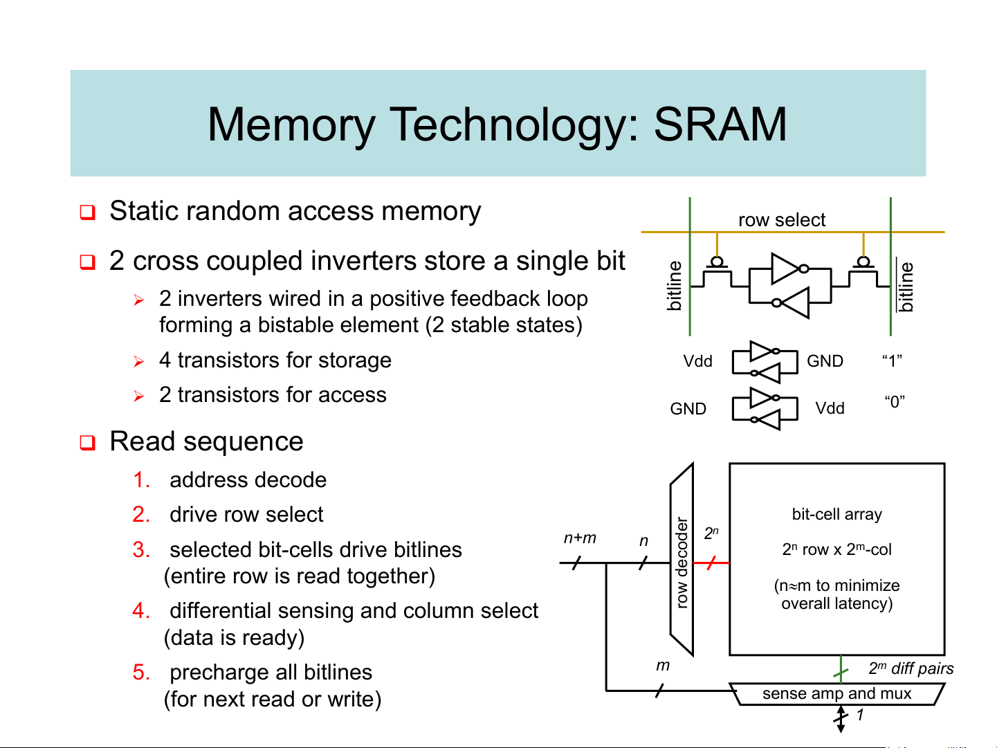
❑ Static random access memory row select
❑ 2 cross coupled inverters store a single bit line line
➢ 2 inverters wired in a positive feedback loop bit bit
forming a bistable element (2 stable states) ➢ 4 transistors for storage Vdd GND “1” ➢ 2 transistors for access GND Vdd “0” ❑ Read sequence 1. address decode 2. drive row select r bit-cell array e d 2n n+m
3. selected bit-cells drive bitlines n co 2n row x 2m-col e (entire row is read together) d w (nm to minimize o
4. differential sensing and column select r overall latency) (data is ready) 5. precharge all bitlines m 2m diff pairs (for next read or write) sense amp and mux 1
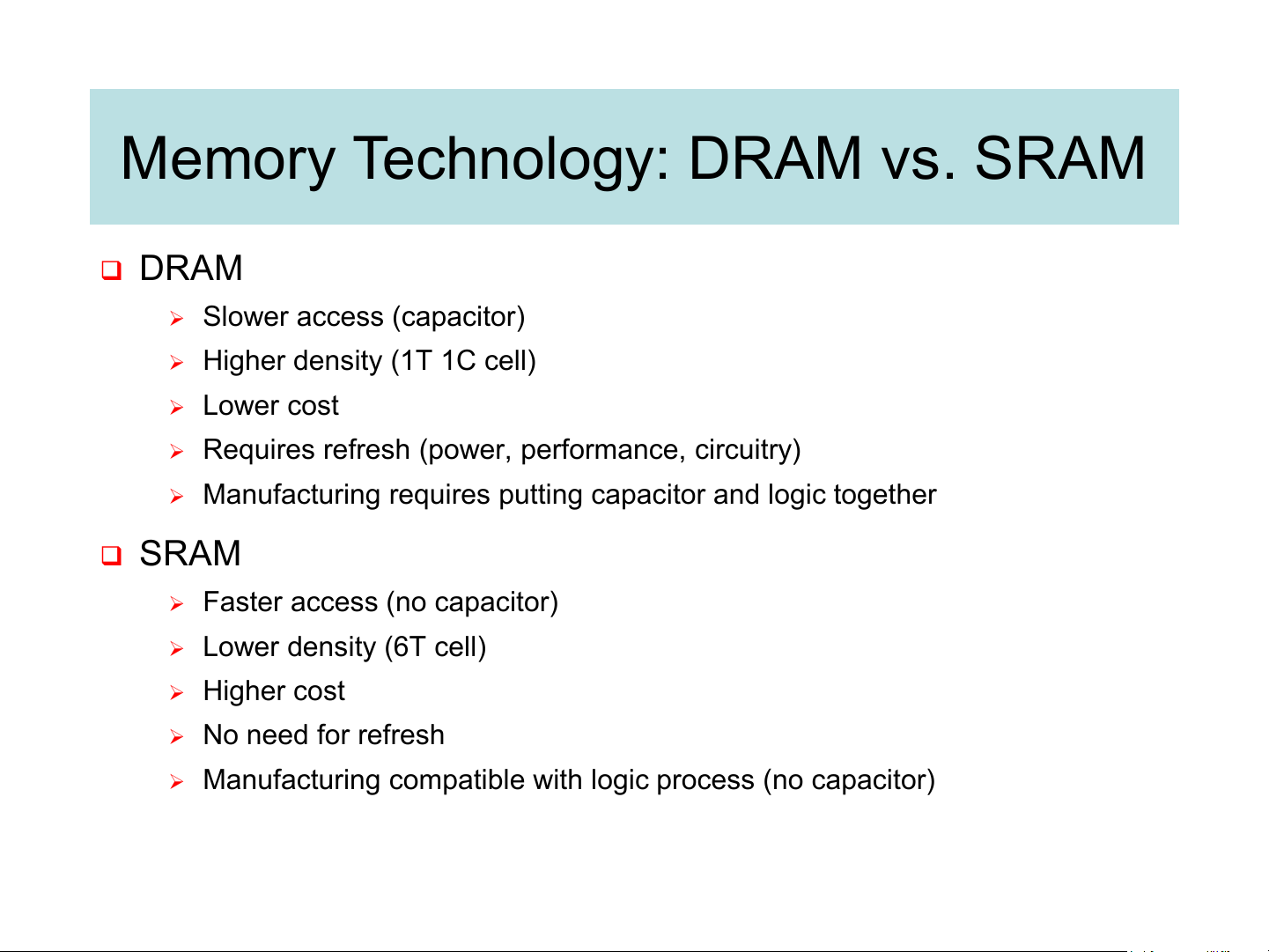
Memory Technology: DRAM vs. SRAM ❑ DRAM ➢ Slower access (capacitor)
➢ Higher density (1T 1C cell) ➢ Lower cost
➢ Requires refresh (power, performance, circuitry)
➢ Manufacturing requires putting capacitor and logic together ❑ SRAM
➢ Faster access (no capacitor) ➢ Lower density (6T cell) ➢ Higher cost ➢ No need for refresh
➢ Manufacturing compatible with logic process (no capacitor)
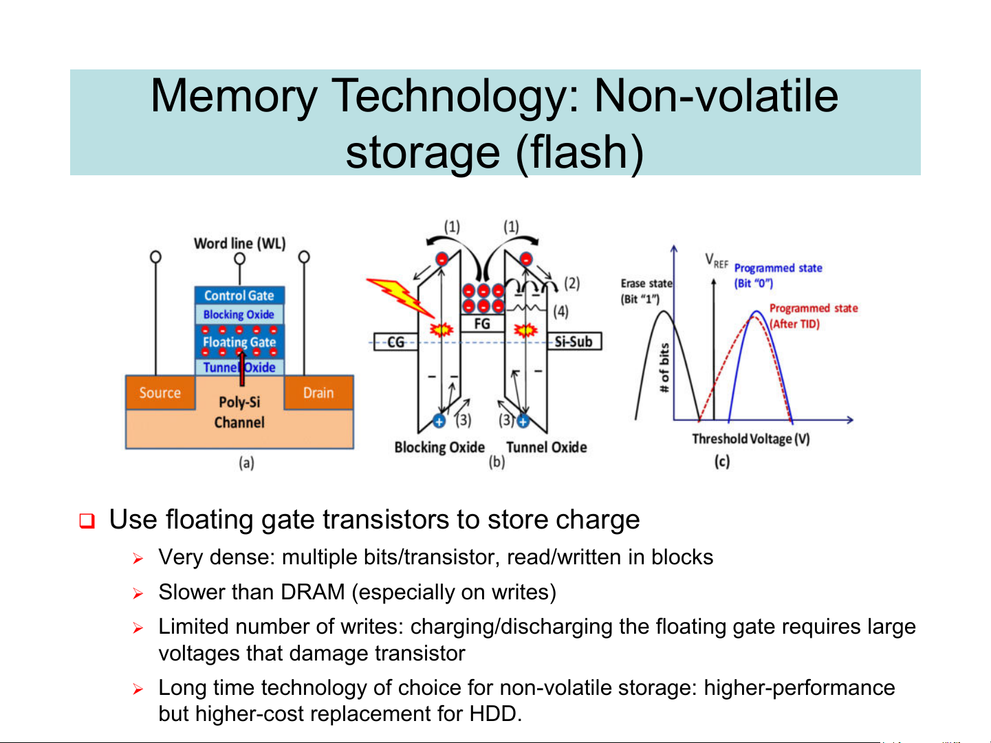
Memory Technology: Non-volatile storage (flash)
❑ Use floating gate transistors to store charge
➢ Very dense: multiple bits/transistor, read/written in blocks
➢ Slower than DRAM (especially on writes)
➢ Limited number of writes: charging/discharging the floating gate requires large
voltages that damage transistor
➢ Long time technology of choice for non-volatile storage: higher-performance
but higher-cost replacement for HDD. Memory hierarchy: the idea ❑ The problem: ➢ Bigger is slower
➢ Faster is more expensive (dollars and chip area)
❑ We want both fast and large
➢ But we cannot achieve both with a single level of memory ❑ Idea:
➢ Have multiple levels of storage (progressively bigger and slower as the
levels are farther from the processor) and ensure most of the data the
processor needs is kept in the fast(er) level(s) ❑ Why Does it Work?
➢ Locality of memory reference: if there’s an access to address 𝑋 at time 𝑡, it’s
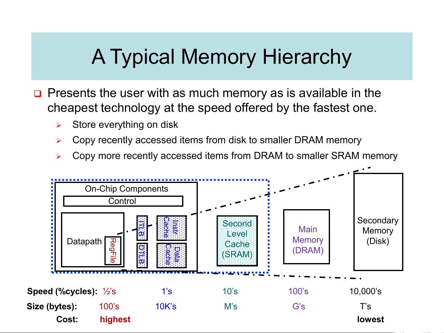
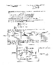
very probable that the program will access a nearby location in the near future. A Typical Memory Hierarchy
❑ Presents the user with as much memory as is available in the
cheapest technology at the speed offered by the fastest one. ➢ Store everything on disk ➢
Copy recently accessed items from disk to smaller DRAM memory ➢
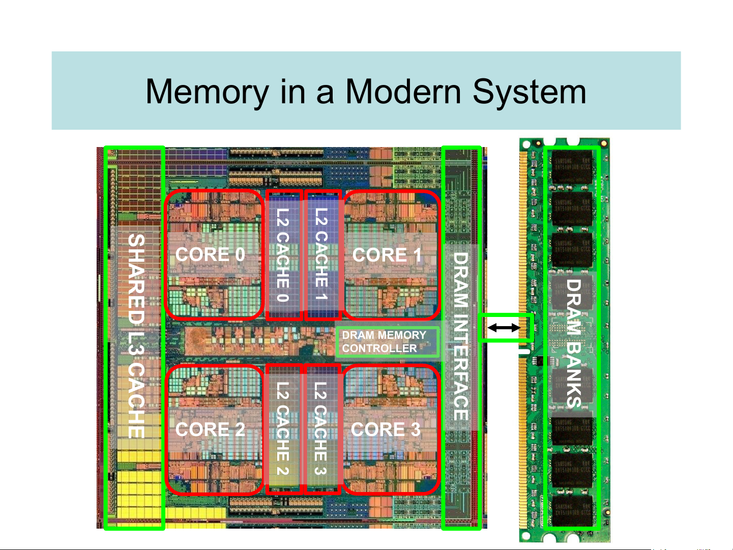
Copy more recently accessed items from DRAM to smaller SRAM memory On-Chip Components Control Cach IT In L str Second Secondary B e Main Reg Level Memory Datapath DT Cach Dat Cache Memory (Disk) Fi (DRAM) le L B a (SRAM) e Speed (%cycles): ½’s 1’s 10’s 100’s 10,000’s Size (bytes): 100’s 10K’s M’s G’s T’s Cost: highest lowest Memory in a Modern System L2 L2 SHA CA CA CHE CHE DR CORE 0 CORE 1 RED AM D 0 1 R INTERF A L3 M DRAM MEMORY B CA CONTROLLER A N L2 L2 AC K CH S CA CA E E CORE 2 CHE CHE CORE 3 2 3 The memory locality principle
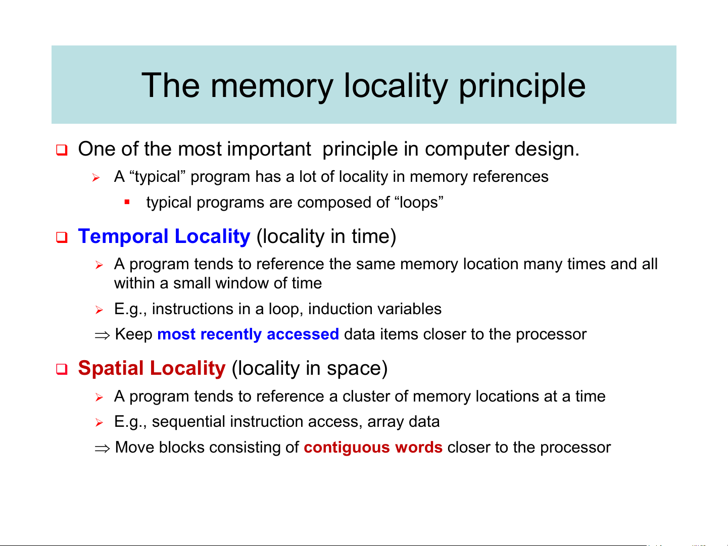
❑ One of the most important principle in computer design.
➢ A “typical” program has a lot of locality in memory references
▪ typical programs are composed of “loops”
❑ Temporal Locality (locality in time)
➢ A program tends to reference the same memory location many times and all within a small window of time
➢ E.g., instructions in a loop, induction variables
Keep most recently accessed data items closer to the processor
❑ Spatial Locality (locality in space)
➢ A program tends to reference a cluster of memory locations at a time
➢ E.g., sequential instruction access, array data
Move blocks consisting of contiguous words closer to the processor Characteristics of the Memory Hierarchy
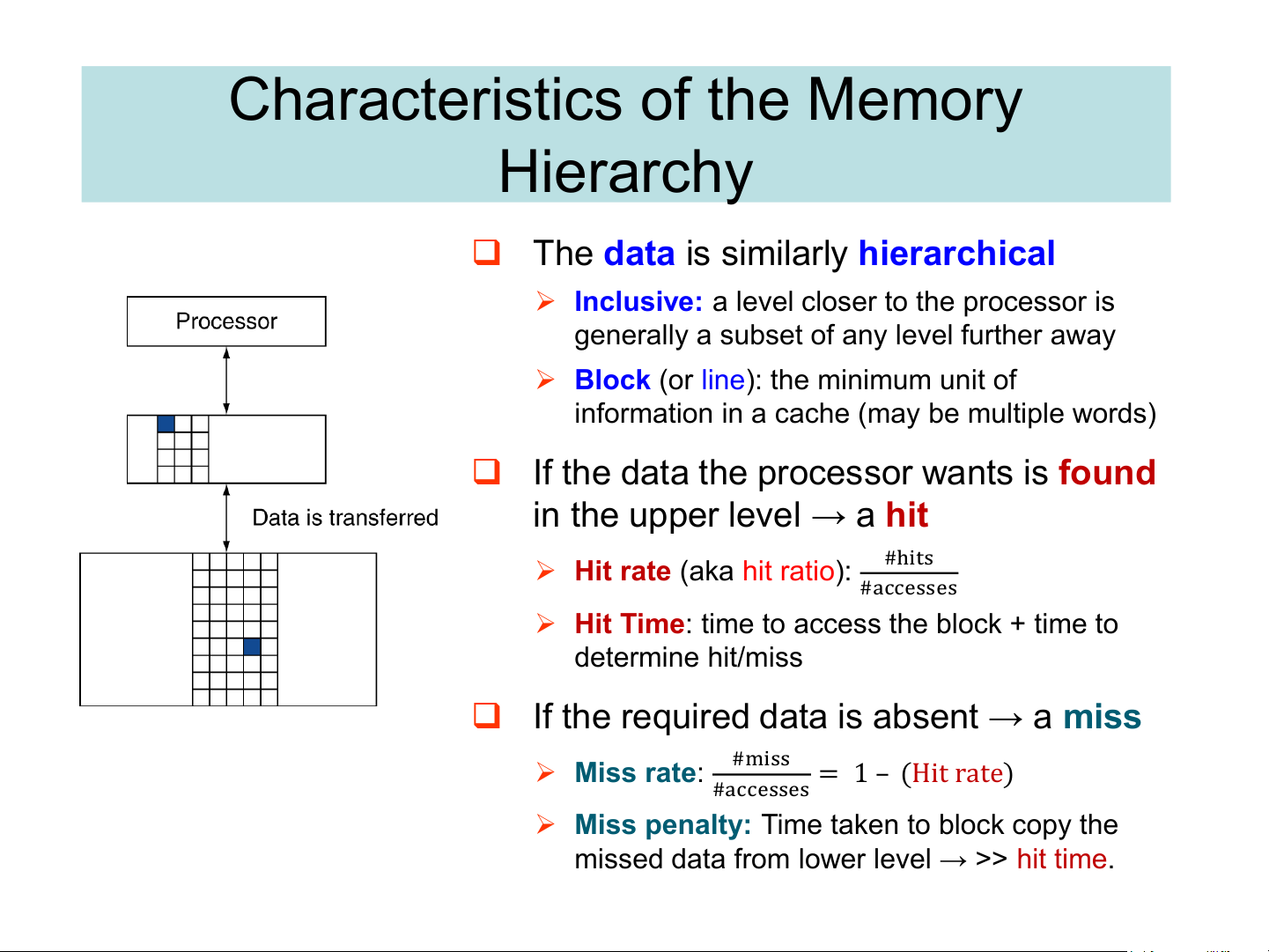
❑ The data is similarly hierarchical
➢ Inclusive: a level closer to the processor is
generally a subset of any level further away
➢ Block (or line): the minimum unit of
information in a cache (may be multiple words)
❑ If the data the processor wants is found
in the upper level → a hit ➢ #hits
Hit rate (aka hit ratio): #accesses
➢ Hit Time: time to access the block + time to determine hit/miss
❑ If the required data is absent → a miss ➢ #miss Miss rate: = 1 – (Hit rate) #accesses
➢ Miss penalty: Time taken to block copy the
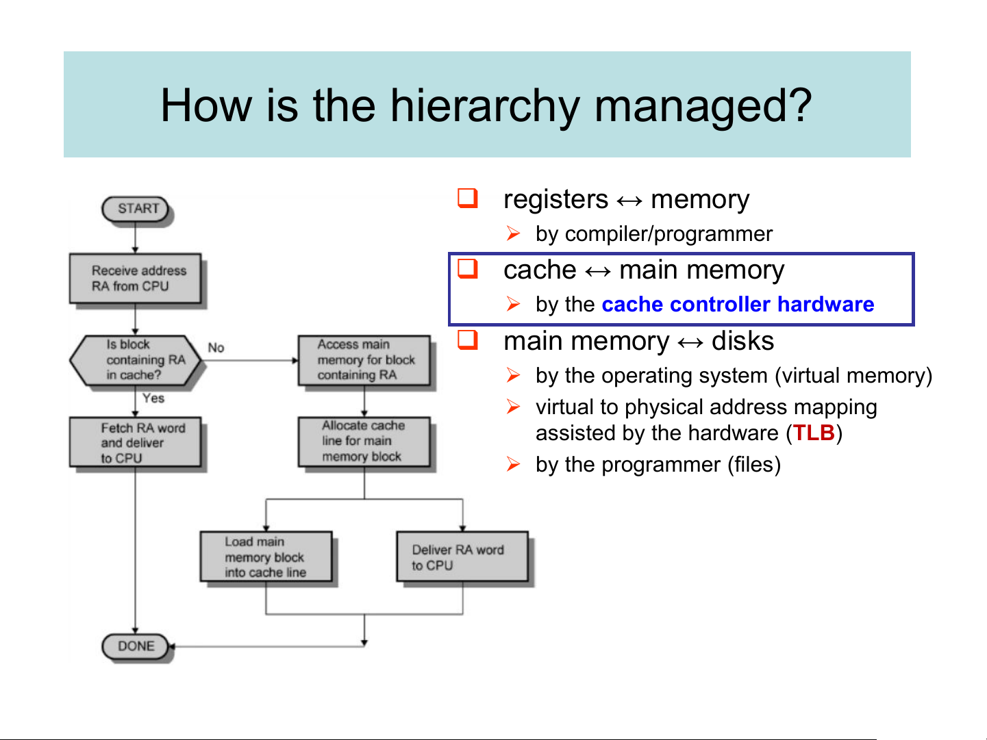
missed data from lower level → >> hit time. How is the hierarchy managed? ❑ registers ↔ memory ➢ by compiler/programmer ❑ cache ↔ main memory
➢ by the cache controller hardware ❑ main memory ↔ disks
➢ by the operating system (virtual memory)
➢ virtual to physical address mapping
assisted by the hardware (TLB) ➢ by the programmer (files) Cache Basics
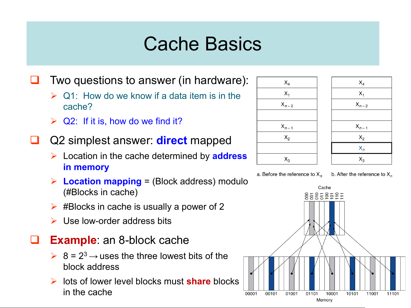
❑ Two questions to answer (in hardware):
➢ Q1: How do we know if a data item is in the cache?
➢ Q2: If it is, how do we find it?
❑ Q2 simplest answer: direct mapped
➢ Location in the cache determined by address in memory
➢ Location mapping = (Block address) modulo (#Blocks in cache)
➢ #Blocks in cache is usually a power of 2 ➢ Use low-order address bits
❑ Example: an 8-block cache
➢ 8 = 23 → uses the three lowest bits of the block address
➢ lots of lower level blocks must share blocks in the cache Tags and Valid Bits
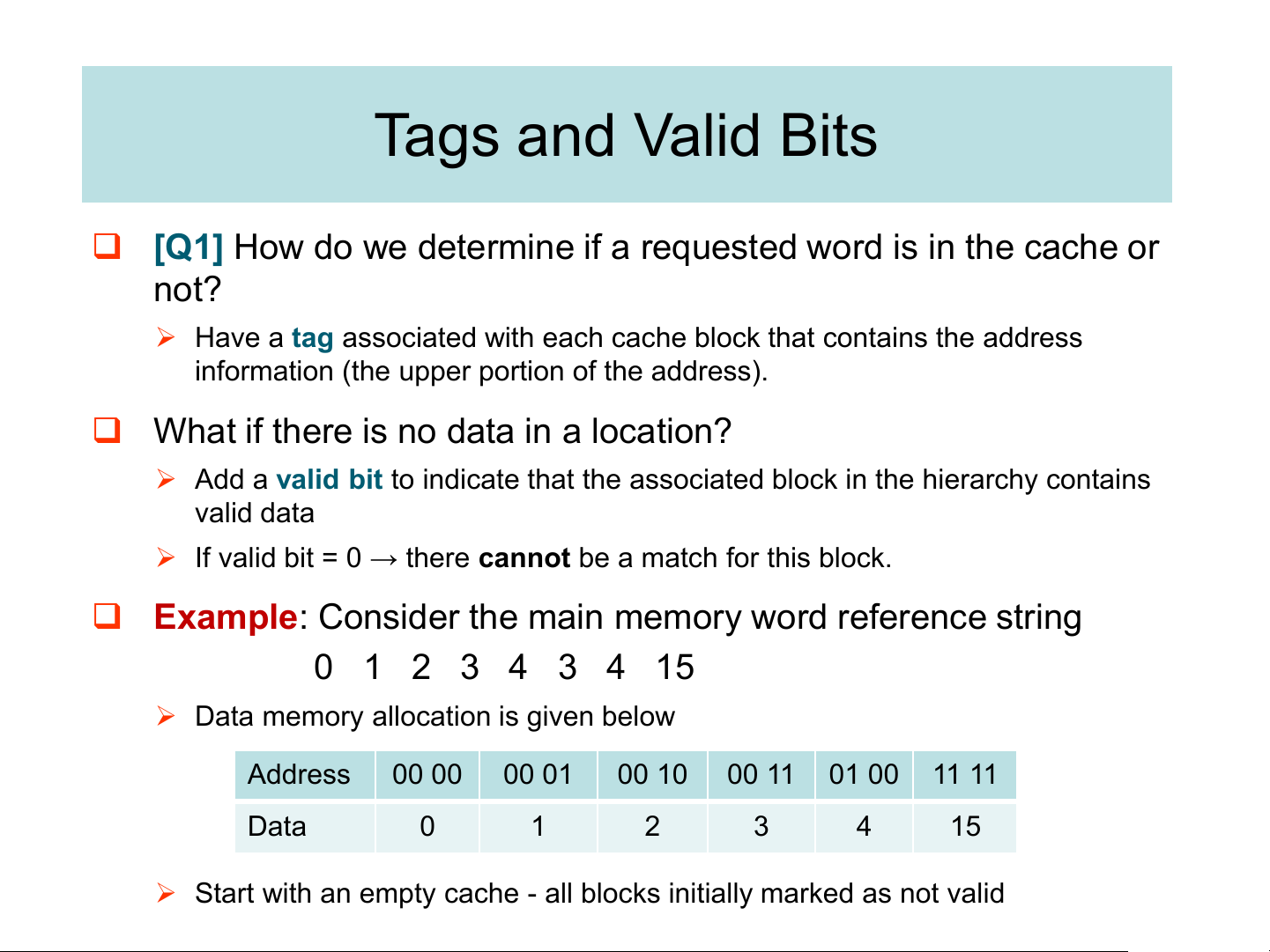
❑ [Q1] How do we determine if a requested word is in the cache or not?
➢ Have a tag associated with each cache block that contains the address
information (the upper portion of the address).
❑ What if there is no data in a location?
➢ Add a valid bit to indicate that the associated block in the hierarchy contains valid data
➢ If valid bit = 0 → there cannot be a match for this block.
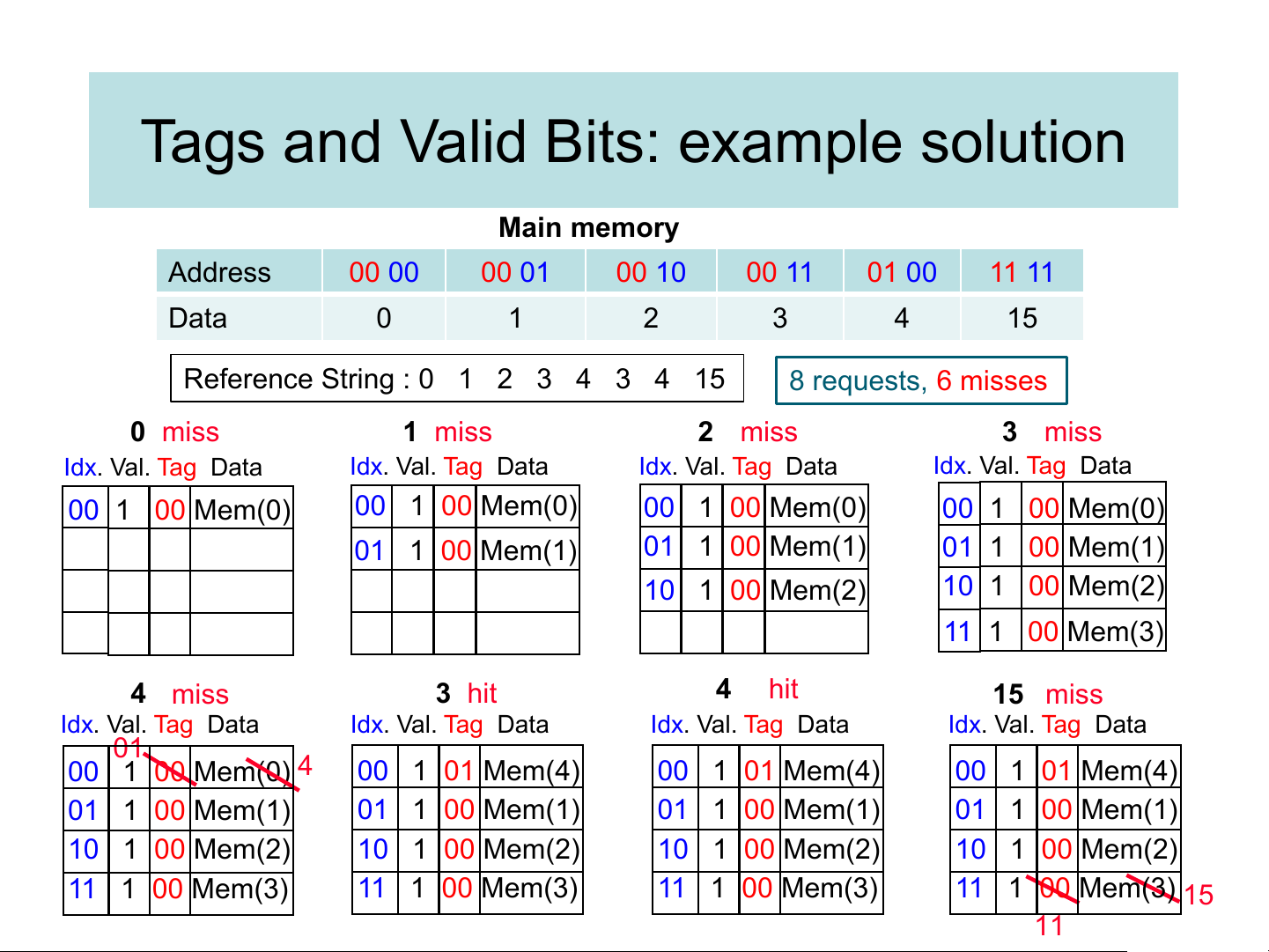
❑ Example: Consider the main memory word reference string 0 1 2 3 4 3 4 15
➢ Data memory allocation is given below Address 00 00 00 01 00 10 00 11 01 00 11 11 Data 0 1 2 3 4 15
➢ Start with an empty cache - all blocks initially marked as not valid
Tags and Valid Bits: example solution Main memory Address 00 00 00 01 00 10 00 11 01 00 11 11 Data 0 1 2 3 4 15
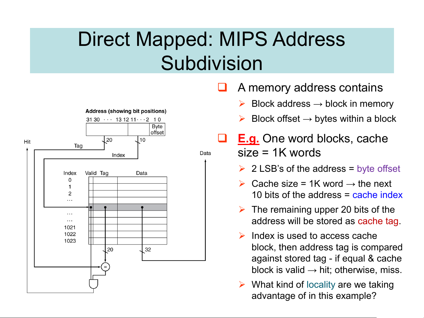
Reference String : 0 1 2 3 4 3 4 15 8 requests, 6 misses 0 miss 1 miss 2 miss 3 miss Idx. Val. Tag Data Idx. Val. Tag Data Idx. Val. Tag Data Idx. Val. Tag Data 00 1 00 Mem(0) 00 1 00 Mem(0) 00 1 00 Mem(0) 00 1 00 Mem(0) 01 1 00 Mem(1) 01 1 00 Mem(1) 01 1 00 Mem(1) 10 1 00 Mem(2) 10 1 00 Mem(2) 11 1 00 Mem(3) 4 miss 3 hit 4 hit 15 miss Idx. Val. Tag Data Idx. Val. Tag Data Idx. Val. Tag Data Idx. Val. Tag Data 01 00 1 00 Mem(0) 4 00 1 01 Mem(4) 00 1 01 Mem(4) 00 1 01 Mem(4) 01 1 00 Mem(1) 01 1 00 Mem(1) 01 1 00 Mem(1) 01 1 00 Mem(1) 10 1 00 Mem(2) 10 1 00 Mem(2) 10 1 00 Mem(2) 10 1 00 Mem(2) 11 1 00 Mem(3) 11 1 00 Mem(3) 11 1 00 Mem(3) 11 1 00 Mem(3) 15 11 Direct Mapped: MIPS Address Subdivision ❑ A memory address contains
➢ Block address → block in memory
➢ Block offset → bytes within a block
❑ E.g. One word blocks, cache size = 1K words
➢ 2 LSB’s of the address = byte offset
➢ Cache size = 1K word → the next
10 bits of the address = cache index
➢ The remaining upper 20 bits of the
address will be stored as cache tag.
➢ Index is used to access cache
block, then address tag is compared
against stored tag - if equal & cache
block is valid → hit; otherwise, miss.
➢ What kind of locality are we taking advantage of in this example? Handling Cache Hits ❑ Read hits (I$ and D$) ➢ Trivial ❑ Write hits (D$ only)
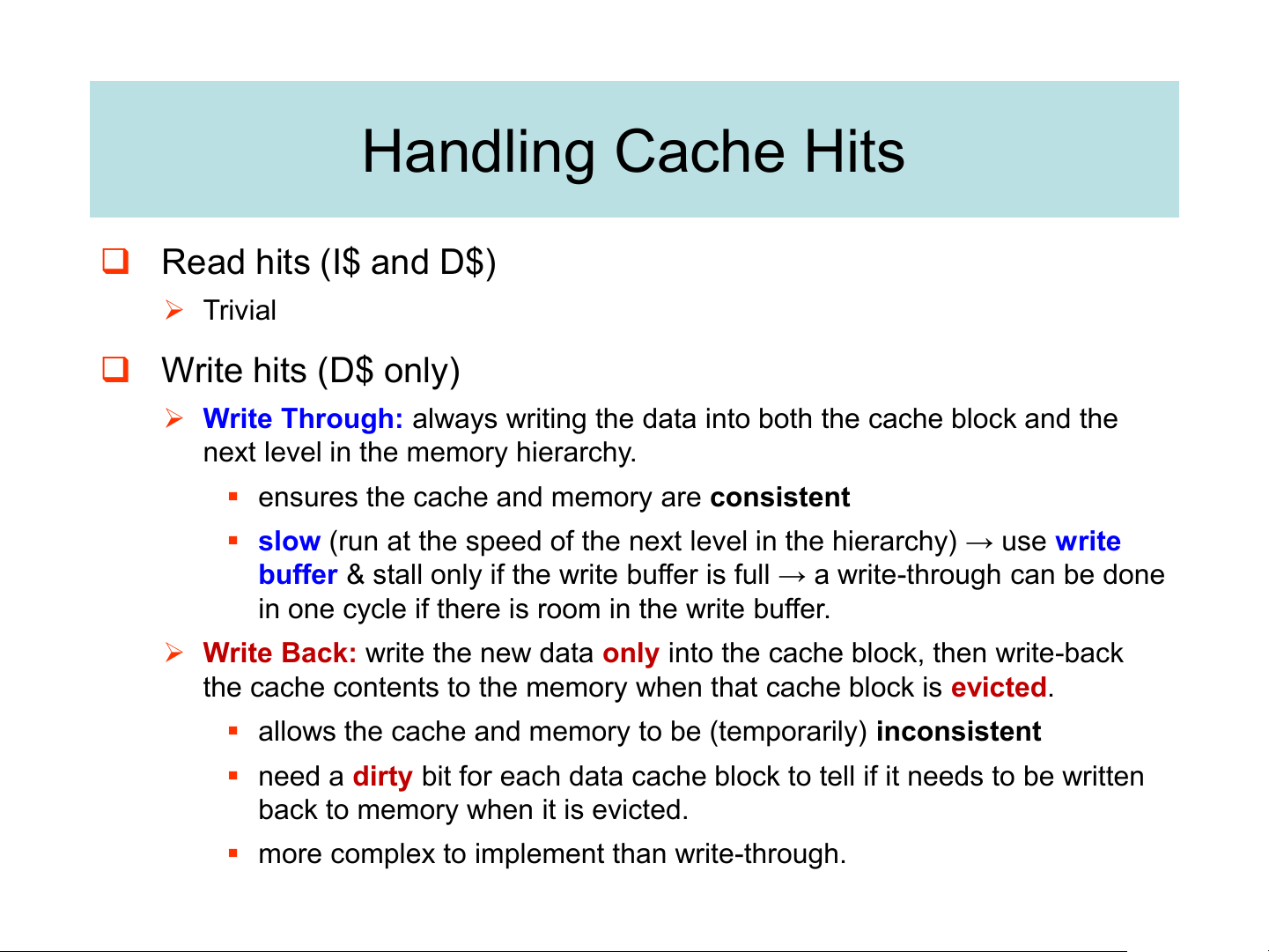
➢ Write Through: always writing the data into both the cache block and the
next level in the memory hierarchy.
▪ ensures the cache and memory are consistent
▪ slow (run at the speed of the next level in the hierarchy) → use write
buffer & stall only if the write buffer is full → a write-through can be done
in one cycle if there is room in the write buffer.
➢ Write Back: write the new data only into the cache block, then write-back
the cache contents to the memory when that cache block is evicted.
▪ allows the cache and memory to be (temporarily) inconsistent
▪ need a dirty bit for each data cache block to tell if it needs to be written
back to memory when it is evicted.
▪ more complex to implement than write-through.
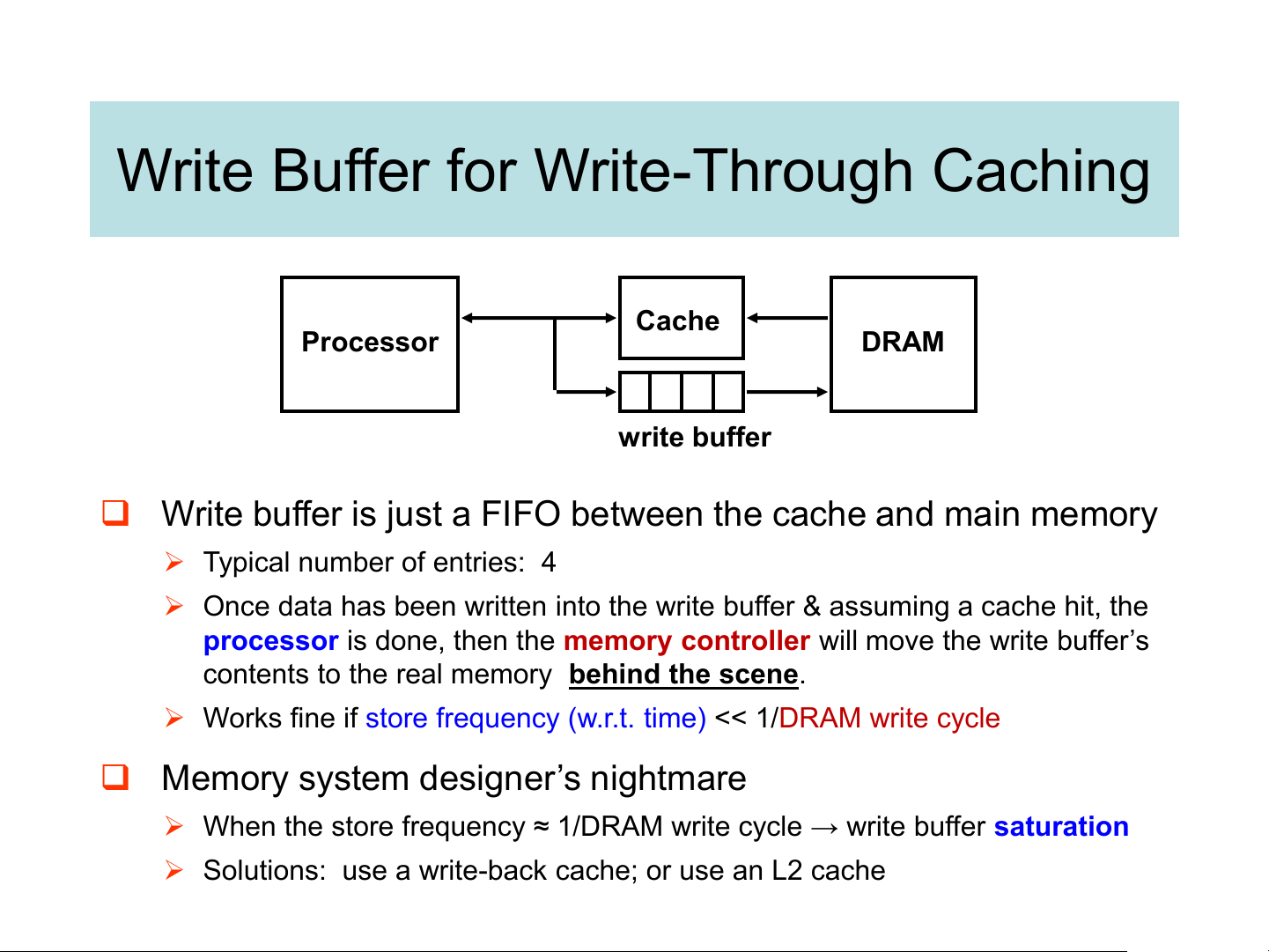
Write Buffer for Write-Through Caching Cache Processor DRAM write buffer
❑ Write buffer is just a FIFO between the cache and main memory
➢ Typical number of entries: 4
➢ Once data has been written into the write buffer & assuming a cache hit, the
processor is done, then the memory controller wil move the write buffer’s
contents to the real memory behind the scene.
➢ Works fine if store frequency (w.r.t. time) << 1/DRAM write cycle
❑ Memory system designer’s nightmare
➢ When the store frequency ≈ 1/DRAM write cycle → write buffer saturation
➢ Solutions: use a write-back cache; or use an L2 cache Direct mapped: conflict miss
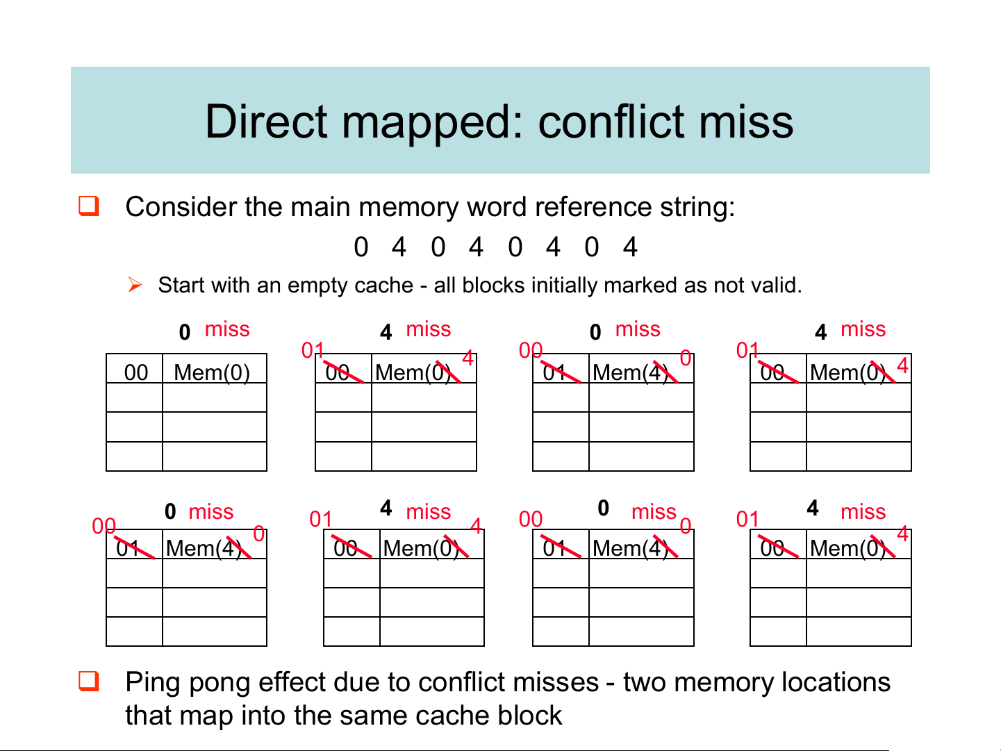
❑ Consider the main memory word reference string: 0 4 0 4 0 4 0 4
➢ Start with an empty cache - all blocks initially marked as not valid. 0 miss 4 miss 0 miss 4 miss 01 4 00 0 01 00 Mem(0) 00 Mem(0) 01 Mem(4) 00 Mem(0) 4 0 miss 4 miss 0 miss 4 miss 01 00 4 00 01 0 0 4 01 Mem(4) 00 Mem(0) 01 Mem(4) 00 Mem(0)
❑ Ping pong effect due to conflict misses - two memory locations
that map into the same cache block
Tài liệu liên quan:
-
Giáo trình Đồ hoạ máy tính môn Kiến trúc máy tính | Trường Đại học Công nghệ, Đại học Quốc gia Hà Nội
23 12 -
TỔNG HỢP ĐỀ THI KTMT
49 25 -
Đề thi Kiến trúc máy tính đề số 2 năm học 2020-2021 | Trường Đại học Công nghệ, Đại học Quốc gia Hà Nội
255 128 -
Đề thi và đáp án Kiến trúc máy tính giữa kỳ 1 năm học 2021-2022 | Trường Đại học Công nghệ, Đại học Quốc gia Hà Nội
262 131 -
Đề thi Kiến trúc máy tính CLC giữa kỳ 1 năm học 2022-2023 | Trường Đại học Công nghệ, Đại học Quốc gia Hà Nội
211 106