SLIDE Week 13 – Lecture 13 – Memory (cont) Kiến Trúc Máy Tính | Trường Đại học Công nghệ, Đại học Quốc gia Hà Nội
SLIDE Week 13 – Lecture 13 – Memory (cont) Kiến Trúc Máy Tính | Trường Đại học Công nghệ, Đại học Quốc gia Hà Nội . Tài liệu được sưu tầm và biên soạn dưới dạng PDF gồm 31 trang giúp bạn tham khảo, củng cố kiến thức và ôn tập đạt kết quả cao trong kỳ thi sắp tới. Mời bạn đọc đón xem!
Môn: Kiến Trúc Máy Tính (UET) 20 tài liệu
Trường: Trường Đại học Công nghệ, Đại học Quốc gia Hà Nội 824 tài liệu
Tác giả:
Preview text:
ELT3047 Computer Architecture Lecture 13: Memory (cont.) Hoang Gia Hung
Faculty of Electronics and Telecommunications
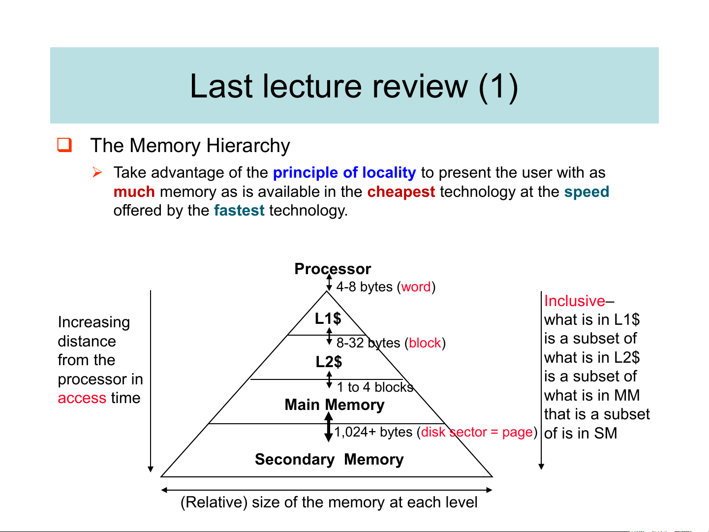
University of Engineering and Technology, VNU Hanoi Last lecture review (1) ❑ The Memory Hierarchy
➢ Take advantage of the principle of locality to present the user with as
much memory as is available in the cheapest technology at the speed
offered by the fastest technology. Processor 4-8 bytes (word) Inclusive– Increasing L1$ what is in L1$ distance is a subset of 8-32 bytes (block) from the L2$ what is in L2$ processor in is a subset of 1 to 4 blocks access time what is in MM Main Memory that is a subset
1,024+ bytes (disk sector = page) of is in SM Secondary Memory
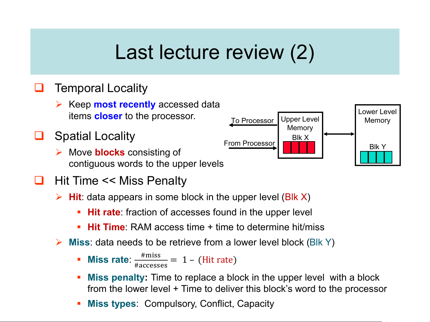
(Relative) size of the memory at each level Last lecture review (2) ❑ Temporal Locality
➢ Keep most recently accessed data
items closer to the processor. Lower Level Upper Level To Processor Memory Memory ❑ Spatial Locality Blk X From Processor ➢ Blk Y
Move blocks consisting of
contiguous words to the upper levels
❑ Hit Time << Miss Penalty
➢ Hit: data appears in some block in the upper level (Blk X)
▪ Hit rate: fraction of accesses found in the upper level
▪ Hit Time: RAM access time + time to determine hit/miss
➢ Miss: data needs to be retrieve from a lower level block (Blk Y) ▪ #miss Miss rate: = 1 – (Hit rate) #accesses
▪ Miss penalty: Time to replace a block in the upper level with a block
from the lower level + Time to deliver this block’s word to the processor
▪ Miss types: Compulsory, Conflict, Capacity Measuring Cache Performance
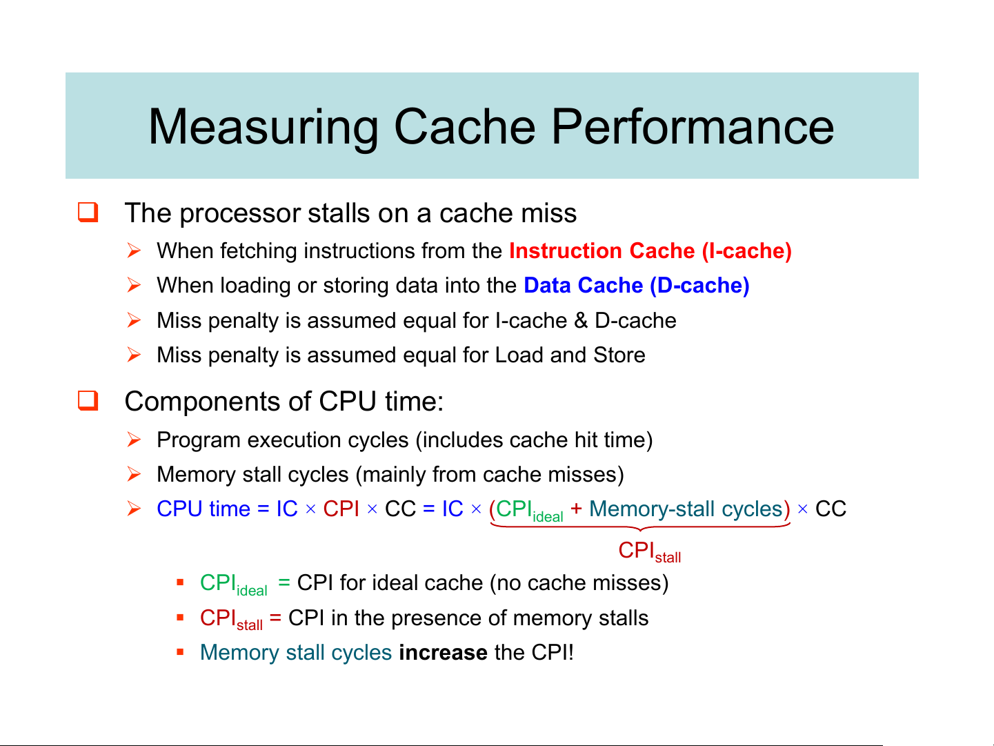
❑ The processor stalls on a cache miss
➢ When fetching instructions from the Instruction Cache (I-cache)
➢ When loading or storing data into the Data Cache (D-cache)
➢ Miss penalty is assumed equal for I-cache & D-cache
➢ Miss penalty is assumed equal for Load and Store ❑ Components of CPU time:
➢ Program execution cycles (includes cache hit time)
➢ Memory stall cycles (mainly from cache misses)
➢ CPU time = IC × CPI × CC = IC × (CPI + Memory-stall cycles) × CC ideal CPIstall ▪ CPI
= CPI for ideal cache (no cache misses) ideal ▪ CPI
= CPI in the presence of memory stalls stall
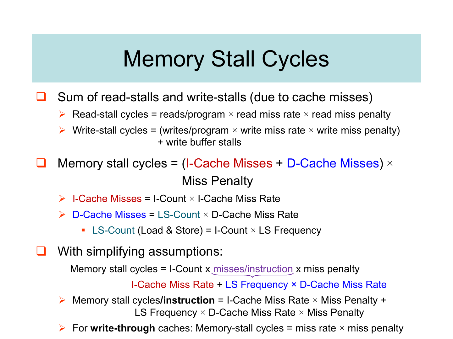
▪ Memory stall cycles increase the CPI! Memory Stall Cycles
❑ Sum of read-stalls and write-stalls (due to cache misses)
➢ Read-stall cycles = reads/program × read miss rate × read miss penalty
➢ Write-stall cycles = (writes/program × write miss rate × write miss penalty) + write buffer stalls
❑ Memory stall cycles = (I-Cache Misses + D-Cache Misses) × Miss Penalty
➢ I-Cache Misses = I-Count × I-Cache Miss Rate
➢ D-Cache Misses = LS-Count × D-Cache Miss Rate
▪ LS-Count (Load & Store) = I-Count × LS Frequency
❑ With simplifying assumptions:
Memory stall cycles = I-Count x misses/instruction x miss penalty
I-Cache Miss Rate + LS Frequency × D-Cache Miss Rate
➢ Memory stall cycles/instruction = I-Cache Miss Rate × Miss Penalty +
LS Frequency × D-Cache Miss Rate × Miss Penalty
➢ For write-through caches: Memory-stall cycles = miss rate × miss penalty Memory Stall Cycles: example
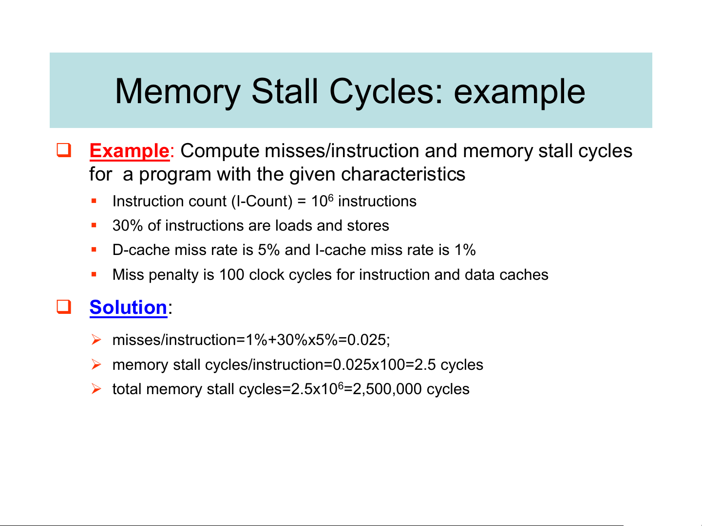
❑ Example: Compute misses/instruction and memory stall cycles
for a program with the given characteristics
▪ Instruction count (I-Count) = 106 instructions
▪ 30% of instructions are loads and stores
▪ D-cache miss rate is 5% and I-cache miss rate is 1%
▪ Miss penalty is 100 clock cycles for instruction and data caches ❑ Solution:
➢ misses/instruction=1%+30%x5%=0.025;
➢ memory stall cycles/instruction=0.025x100=2.5 cycles
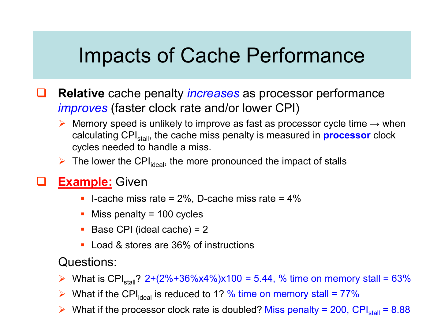
➢ total memory stall cycles=2.5x106=2,500,000 cycles Impacts of Cache Performance
❑ Relative cache penalty increases as processor performance
improves (faster clock rate and/or lower CPI)
➢ Memory speed is unlikely to improve as fast as processor cycle time → when calculating CPI
, the cache miss penalty is measured in stall processor clock
cycles needed to handle a miss. ➢ The lower the CPI
, the more pronounced the impact of stalls ideal ❑ Example: Given
▪ I-cache miss rate = 2%, D-cache miss rate = 4% ▪ Miss penalty = 100 cycles ▪ Base CPI (ideal cache) = 2
▪ Load & stores are 36% of instructions Questions: ➢ What is CPI
? 2+(2%+36%x4%)x100 = 5.44, % time on memory stall = 63% stall ➢ What if the CPI
is reduced to 1? % time on memory stall = 77% ideal
➢ What if the processor clock rate is doubled? Miss penalty = 200, CPI = 8.88 stall
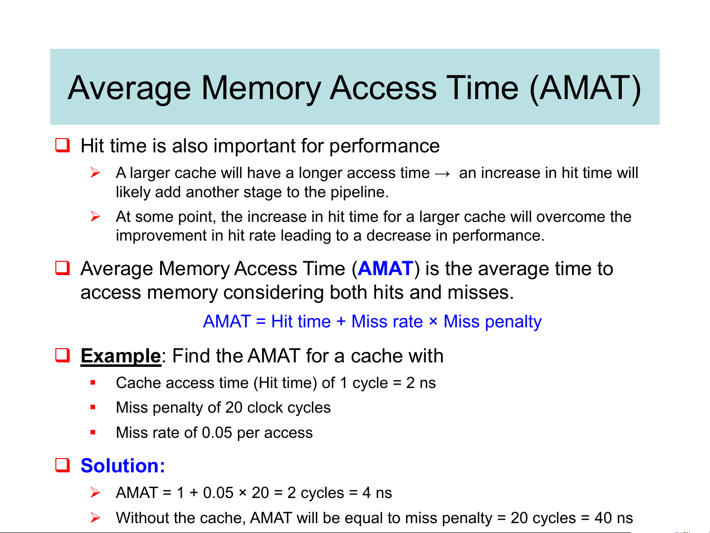
Average Memory Access Time (AMAT)
❑ Hit time is also important for performance
➢ A larger cache wil have a longer access time → an increase in hit time wil
likely add another stage to the pipeline.
➢ At some point, the increase in hit time for a larger cache will overcome the
improvement in hit rate leading to a decrease in performance.
❑ Average Memory Access Time (AMAT) is the average time to
access memory considering both hits and misses.
AMAT = Hit time + Miss rate × Miss penalty
❑ Example: Find the AMAT for a cache with ▪
Cache access time (Hit time) of 1 cycle = 2 ns ▪
Miss penalty of 20 clock cycles ▪ Miss rate of 0.05 per access ❑ Solution:
➢ AMAT = 1 + 0.05 × 20 = 2 cycles = 4 ns
➢ Without the cache, AMAT will be equal to miss penalty = 20 cycles = 40 ns
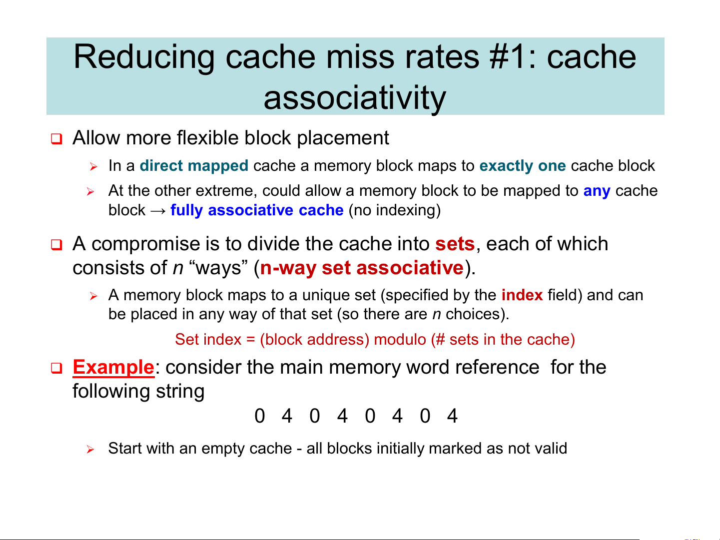
Reducing cache miss rates #1: cache associativity
❑ Allow more flexible block placement
➢ In a direct mapped cache a memory block maps to exactly one cache block
➢ At the other extreme, could allow a memory block to be mapped to any cache
block → fully associative cache (no indexing)
❑ A compromise is to divide the cache into sets, each of which
consists of n “ways” (n-way set associative).
➢ A memory block maps to a unique set (specified by the index field) and can
be placed in any way of that set (so there are n choices).
Set index = (block address) modulo (# sets in the cache)
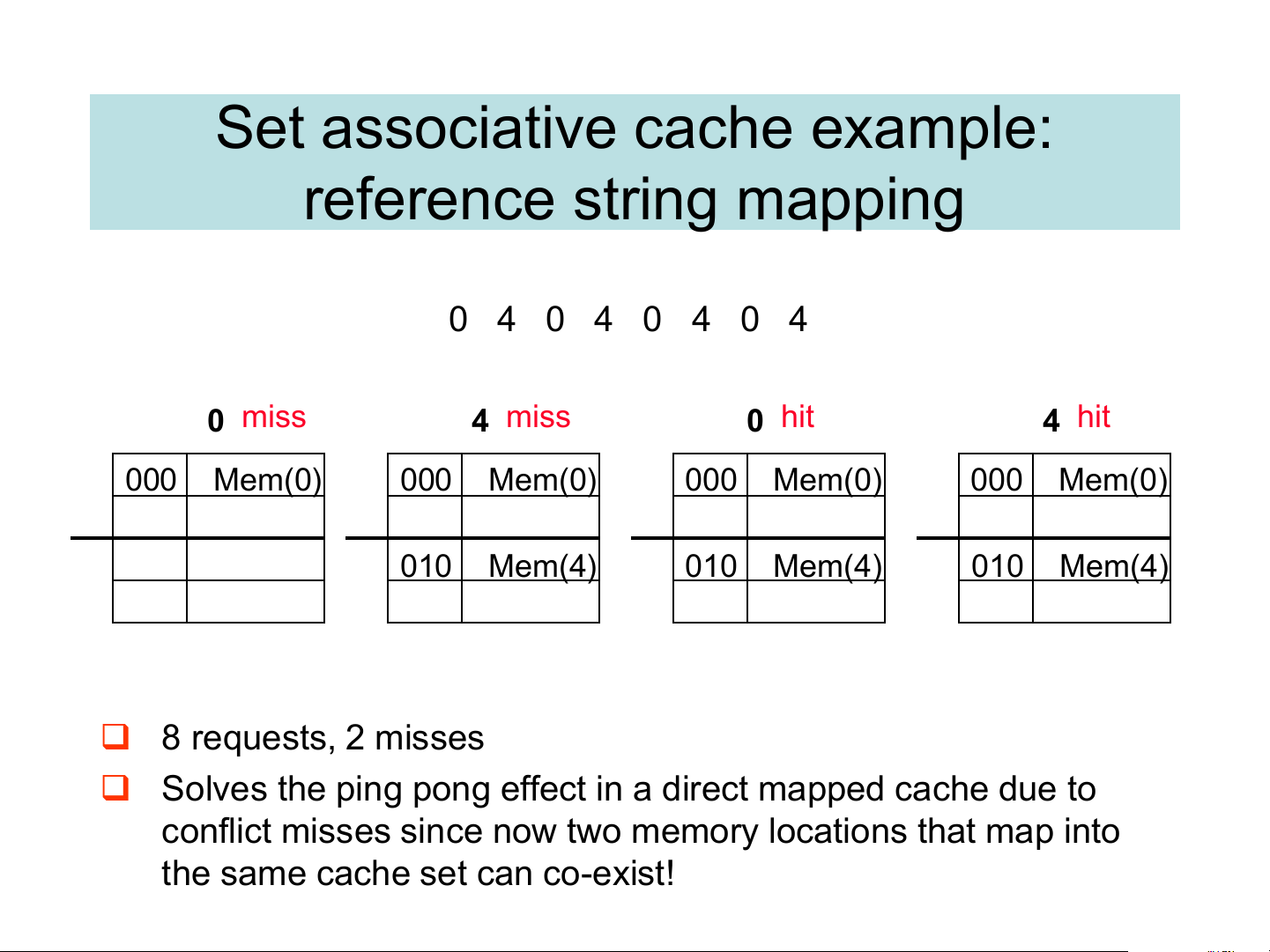
❑ Example: consider the main memory word reference for the following string 0 4 0 4 0 4 0 4
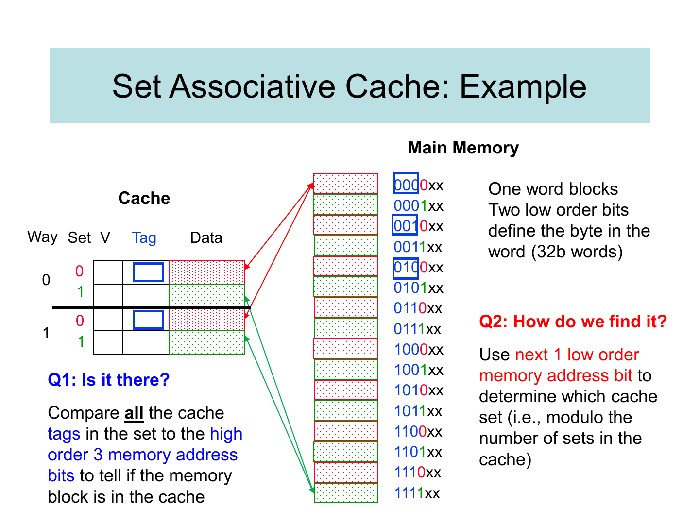
➢ Start with an empty cache - all blocks initially marked as not valid Set Associative Cache: Example Main Memory 0000xx One word blocks Cache 0001xx Two low order bits 0010xx Way Set V Tag Data define the byte in the 0011xx word (32b words) 0 0100xx 0 0101xx 1 0110xx 0 Q2: How do we find it? 0111xx 1 1 1000xx Use next 1 low order 1001xx memory address bit to Q1: Is it there? 1010xx determine which cache Compare all the cache 1011xx set (i.e., modulo the tags in the set to the high 1100xx number of sets in the order 3 memory address 1101xx cache) bits to tell if the memory 1110xx block is in the cache 1111xx
Set associative cache example: reference string mapping 0 4 0 4 0 4 0 4 0 miss 4 miss 0 hit 4 hit 000 Mem(0) 000 Mem(0) 000 Mem(0) 000 Mem(0) 010 Mem(4) 010 Mem(4) 010 Mem(4) ❑ 8 requests, 2 misses
❑ Solves the ping pong effect in a direct mapped cache due to
conflict misses since now two memory locations that map into
the same cache set can co-exist!
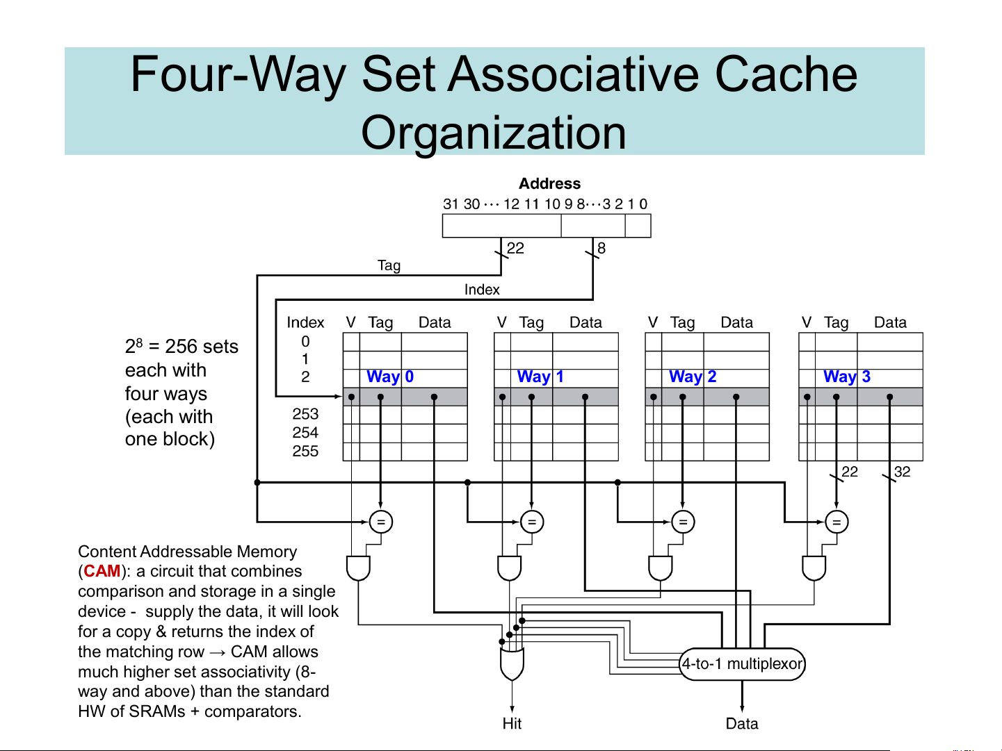
Four-Way Set Associative Cache Organization 28 = 256 sets each with Way 0 Way 1 Way 2 Way 3 four ways (each with one block) Content Addressable Memory
(CAM): a circuit that combines
comparison and storage in a single
device - supply the data, it will look
for a copy & returns the index of
the matching row → CAM allows
much higher set associativity (8-
way and above) than the standard HW of SRAMs + comparators.
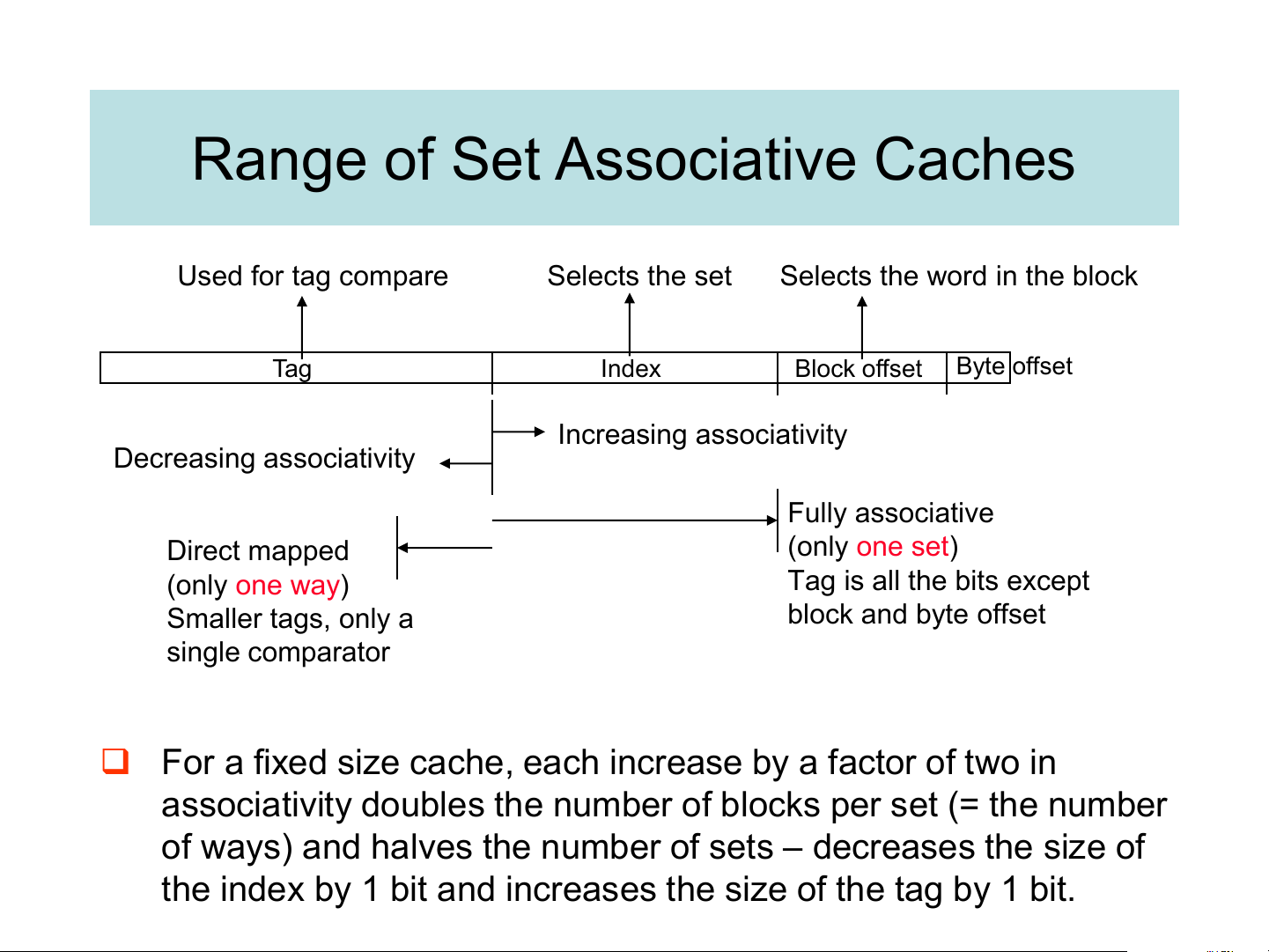
Range of Set Associative Caches Used for tag compare Selects the set Selects the word in the block Tag Index Block offset Byte offset Increasing associativity Decreasing associativity Fully associative Direct mapped (only one set) (only one way) Tag is all the bits except Smaller tags, only a block and byte offset single comparator
❑ For a fixed size cache, each increase by a factor of two in
associativity doubles the number of blocks per set (= the number
of ways) and halves the number of sets – decreases the size of
the index by 1 bit and increases the size of the tag by 1 bit. Replacement Policy
❑ A miss occurred, which way’s block do we pick for replacement?
➢ Direct mapped: no choice.
➢ Set associative: non-valid entry, then choose among entries in the set.
❑ First In First Out (FIFO): replace the oldest block in set
➢ Use one counter per set to specify the oldest block. On a cache miss replace
the block specified by counter & increment the counter.
❑ Least Recently Used (LRU): replace the one that has been unused for the longest time
➢ Requires hardware to keep track of when each way’s block was used relative
to the other blocks in the set. For 2-way set associative, takes one bit per set
→ set the bit when a block is referenced (and reset the other way’s bit)
➢ Manageable for 4-way, too hard beyond that. ❑ Random
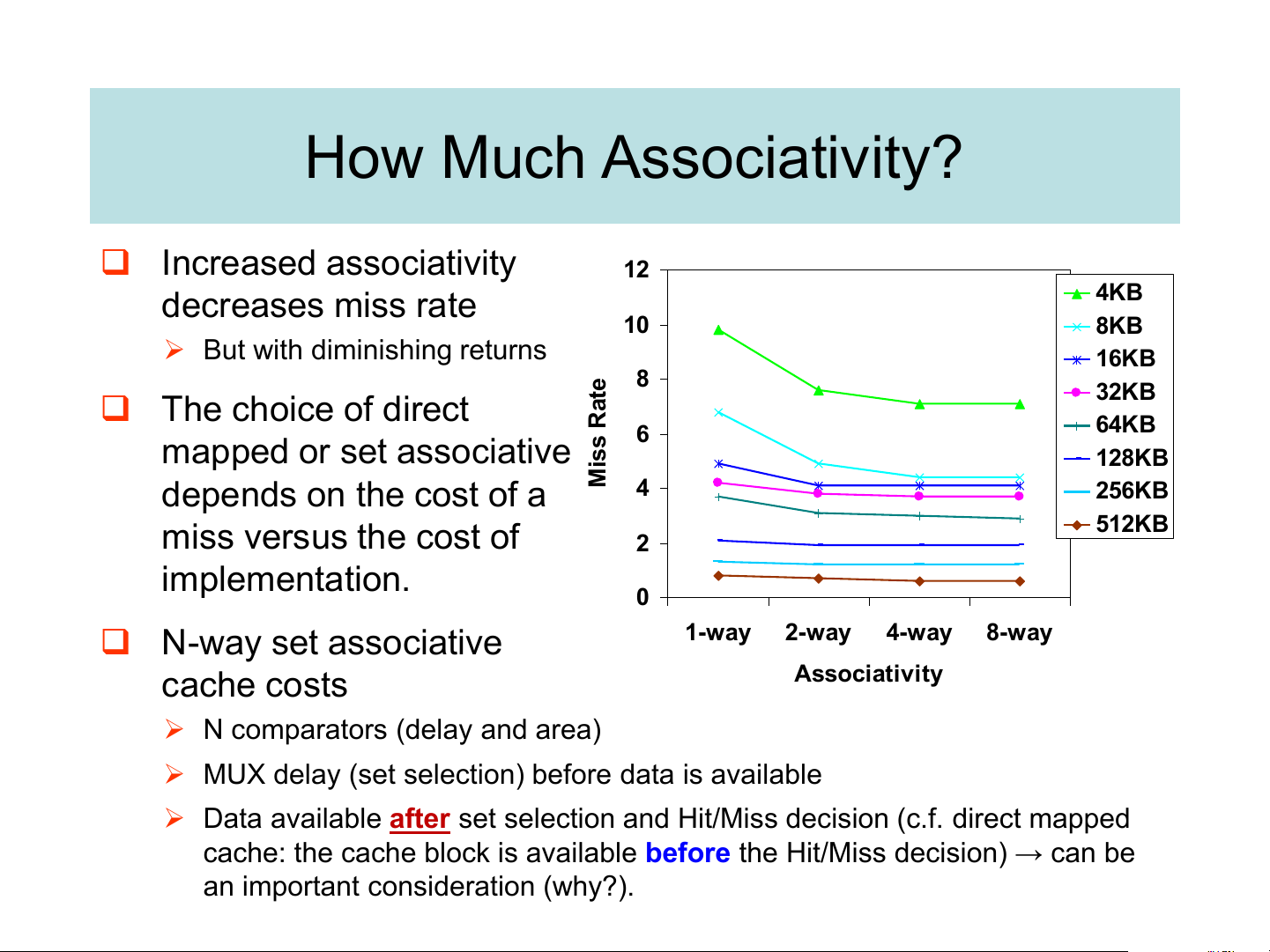
➢ Gives approximately the same performance as LRU for high associativity. How Much Associativity? ❑ Increased associativity 12 4KB decreases miss rate 10 8KB
➢ But with diminishing returns 16KB e 8 t 32KB a ❑ The choice of direct R 6 64KB s
mapped or set associative si 128KB M 4 256KB depends on the cost of a 512KB miss versus the cost of 2 implementation. 0 1-way 2-way 4-way 8-way ❑ N-way set associative Associativity cache costs
➢ N comparators (delay and area)
➢ MUX delay (set selection) before data is available
➢ Data available after set selection and Hit/Miss decision (c.f. direct mapped
cache: the cache block is available before the Hit/Miss decision) → can be
an important consideration (why?).
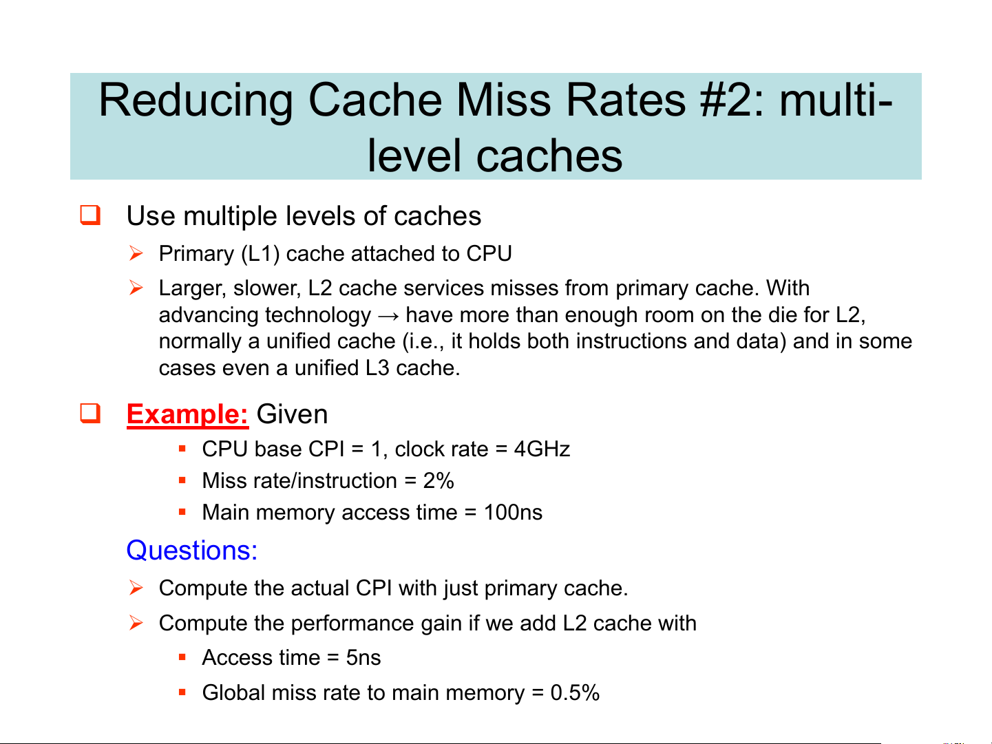
Reducing Cache Miss Rates #2: multi- level caches
❑ Use multiple levels of caches
➢ Primary (L1) cache attached to CPU
➢ Larger, slower, L2 cache services misses from primary cache. With
advancing technology → have more than enough room on the die for L2,
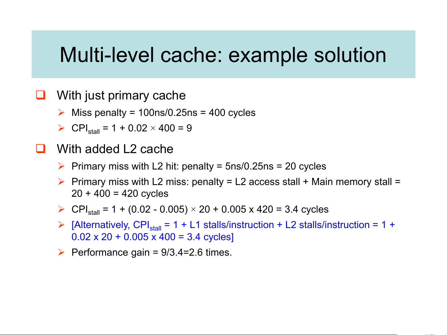
normally a unified cache (i.e., it holds both instructions and data) and in some cases even a unified L3 cache. ❑ Example: Given
▪ CPU base CPI = 1, clock rate = 4GHz ▪ Miss rate/instruction = 2%
▪ Main memory access time = 100ns Questions:
➢ Compute the actual CPI with just primary cache.
➢ Compute the performance gain if we add L2 cache with ▪ Access time = 5ns
▪ Global miss rate to main memory = 0.5%
Multi-level cache: example solution ❑ With just primary cache
➢ Miss penalty = 100ns/0.25ns = 400 cycles ➢ CPI = 1 + 0.02 × 400 = 9 stall ❑ With added L2 cache
➢ Primary miss with L2 hit: penalty = 5ns/0.25ns = 20 cycles
➢ Primary miss with L2 miss: penalty = L2 access stall + Main memory stall = 20 + 400 = 420 cycles ➢ CPI
= 1 + (0.02 - 0.005) × 20 + 0.005 x 420 = 3.4 cycles stall ➢ [Alternatively, CPI
= 1 + L1 stalls/instruction + L2 stalls/instruction = 1 + stall
0.02 x 20 + 0.005 x 400 = 3.4 cycles]
➢ Performance gain = 9/3.4=2.6 times.
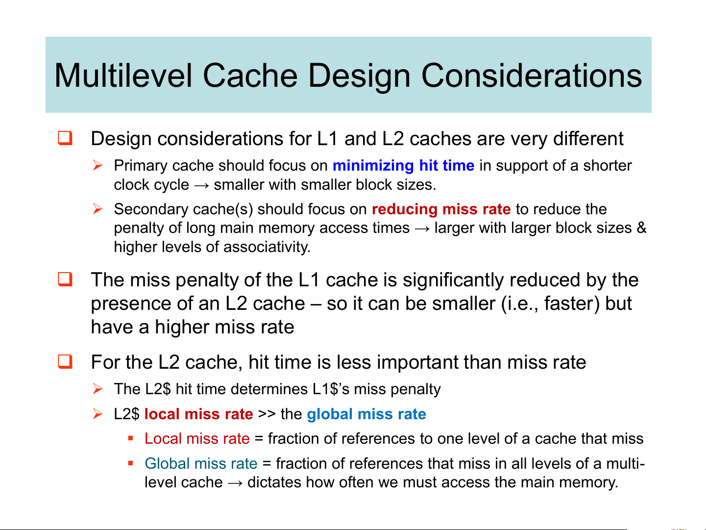
Multilevel Cache Design Considerations
❑ Design considerations for L1 and L2 caches are very different
➢ Primary cache should focus on minimizing hit time in support of a shorter
clock cycle → smaller with smaller block sizes.
➢ Secondary cache(s) should focus on reducing miss rate to reduce the
penalty of long main memory access times → larger with larger block sizes &
higher levels of associativity.
❑ The miss penalty of the L1 cache is significantly reduced by the
presence of an L2 cache – so it can be smaller (i.e., faster) but have a higher miss rate
❑ For the L2 cache, hit time is less important than miss rate
➢ The L2$ hit time determines L1$’s miss penalty
➢ L2$ local miss rate >> the global miss rate
▪ Local miss rate = fraction of references to one level of a cache that miss
▪ Global miss rate = fraction of references that miss in all levels of a multi-
level cache → dictates how often we must access the main memory.
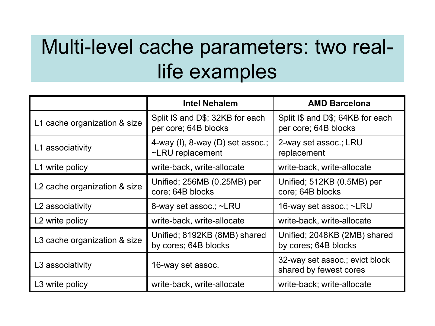
Multi-level cache parameters: two real- life examples Intel Nehalem AMD Barcelona
Split I$ and D$; 32KB for each
Split I$ and D$; 64KB for each
L1 cache organization & size per core; 64B blocks per core; 64B blocks
4-way (I), 8-way (D) set assoc.; 2-way set assoc.; LRU L1 associativity ~LRU replacement replacement L1 write policy write-back, write-allocate write-back, write-allocate Unified; 256MB (0.25MB) per Unified; 512KB (0.5MB) per
L2 cache organization & size core; 64B blocks core; 64B blocks L2 associativity 8-way set assoc.; ~LRU 16-way set assoc.; ~LRU L2 write policy write-back, write-allocate write-back, write-allocate Unified; 8192KB (8MB) shared Unified; 2048KB (2MB) shared
L3 cache organization & size by cores; 64B blocks by cores; 64B blocks
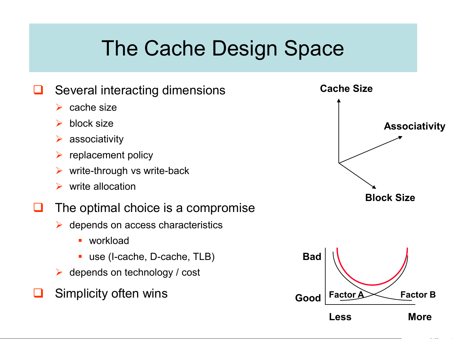
32-way set assoc.; evict block L3 associativity 16-way set assoc. shared by fewest cores L3 write policy write-back, write-allocate write-back; write-allocate The Cache Design Space Cache Size
❑ Several interacting dimensions ➢ cache size ➢ block size Associativity ➢ associativity ➢ replacement policy
➢ write-through vs write-back ➢ write allocation Block Size
❑ The optimal choice is a compromise
➢ depends on access characteristics ▪ workload
▪ use (I-cache, D-cache, TLB) Bad
➢ depends on technology / cost ❑ Simplicity often wins Good Factor A Factor B Less More
Tài liệu liên quan:
-

Giáo trình Đồ hoạ máy tính môn Kiến trúc máy tính | Trường Đại học Công nghệ, Đại học Quốc gia Hà Nội
21 11 -
TỔNG HỢP ĐỀ THI KTMT
48 24 -
Đề thi Kiến trúc máy tính đề số 2 năm học 2020-2021 | Trường Đại học Công nghệ, Đại học Quốc gia Hà Nội
254 127 -
Đề thi và đáp án Kiến trúc máy tính giữa kỳ 1 năm học 2021-2022 | Trường Đại học Công nghệ, Đại học Quốc gia Hà Nội
261 131 -
Đề thi Kiến trúc máy tính CLC giữa kỳ 1 năm học 2022-2023 | Trường Đại học Công nghệ, Đại học Quốc gia Hà Nội
209 105