SLIDE Week 7 – Lecture 7 – Single Cycle Processor Design Kiến Trúc Máy Tính | Trường Đại học Công nghệ, Đại học Quốc gia Hà Nội
SLIDE Week 7 – Lecture 7 – Single Cycle Processor Design Kiến Trúc Máy Tính | Trường Đại học Công nghệ, Đại học Quốc gia Hà Nội . Tài liệu được sưu tầm và biên soạn dưới dạng PDF gồm 39 trang giúp bạn tham khảo, củng cố kiến thức và ôn tập đạt kết quả cao trong kỳ thi sắp tới. Mời bạn đọc đón xem!
Môn: Kiến Trúc Máy Tính (UET) 19 tài liệu
Trường: Trường Đại học Công nghệ, Đại học Quốc gia Hà Nội 762 tài liệu
Tác giả:
Preview text:
ELT3047 Computer Architecture
Lecture 7: Single Cycle Processor Design Hoang Gia Hung
Faculty of Electronics and Telecommunications
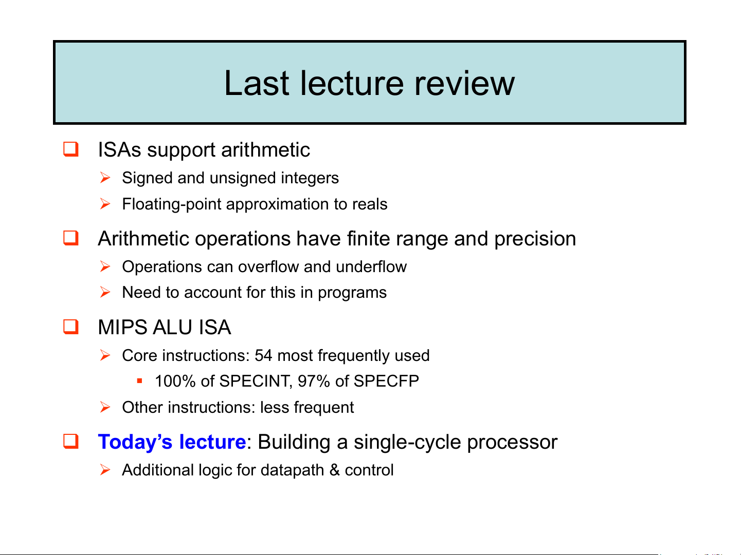
University of Engineering and Technology, VNU Hanoi Last lecture review ❑ ISAs support arithmetic
➢ Signed and unsigned integers
➢ Floating-point approximation to reals
❑ Arithmetic operations have finite range and precision
➢ Operations can overflow and underflow
➢ Need to account for this in programs ❑ MIPS ALU ISA
➢ Core instructions: 54 most frequently used
▪ 100% of SPECINT, 97% of SPECFP
➢ Other instructions: less frequent
❑ Today’s lecture: Building a single-cycle processor
➢ Additional logic for datapath & control
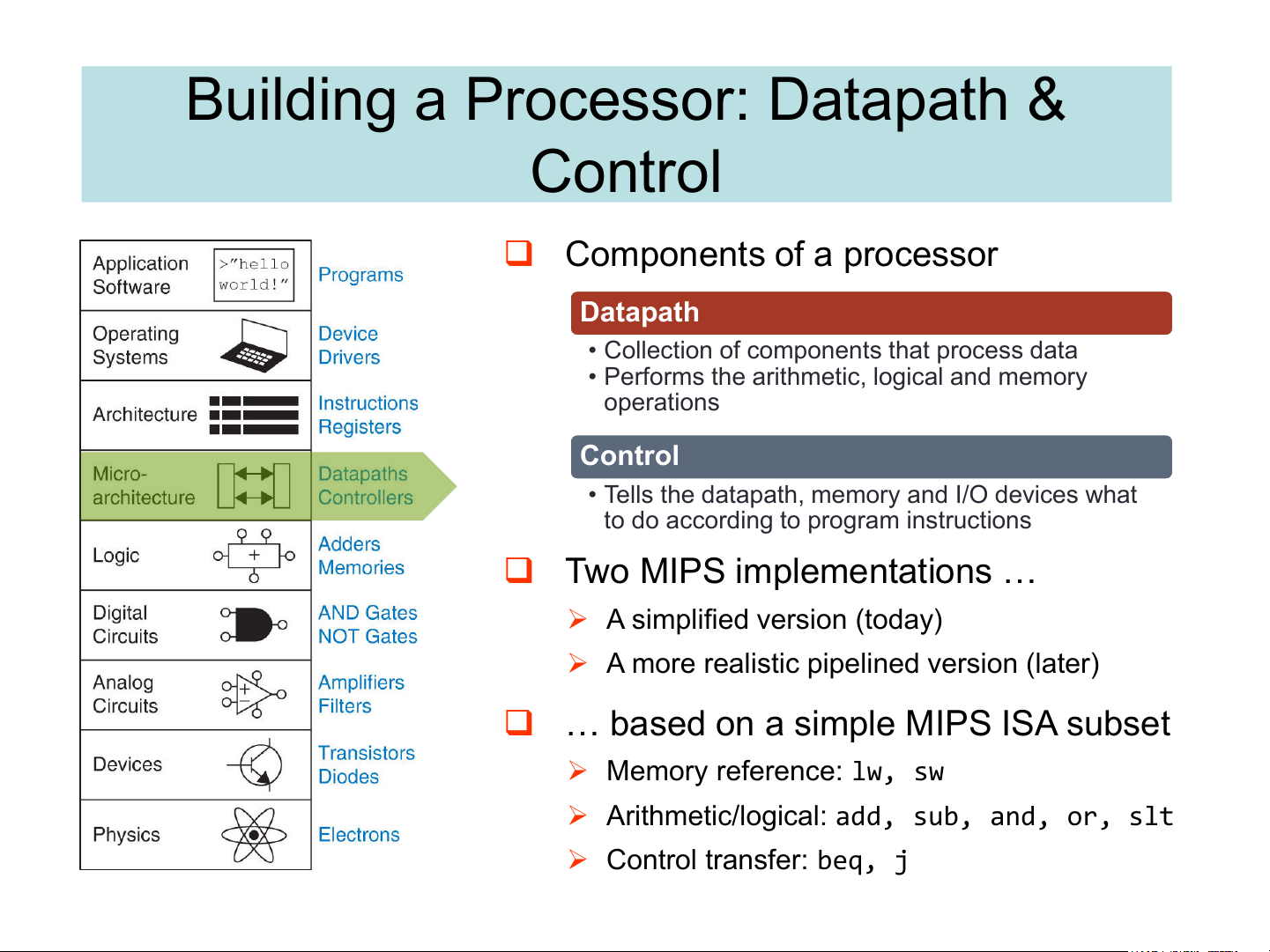
Building a Processor: Datapath & Control ❑ Components of a processor Datapath
• Collection of components that process data
• Performs the arithmetic, logical and memory operations Control
• Tells the datapath, memory and I/O devices what
to do according to program instructions
❑ Two MIPS implementations …
➢ A simplified version (today)
➢ A more realistic pipelined version (later)
❑ … based on a simple MIPS ISA subset ➢ Memory reference: lw, sw
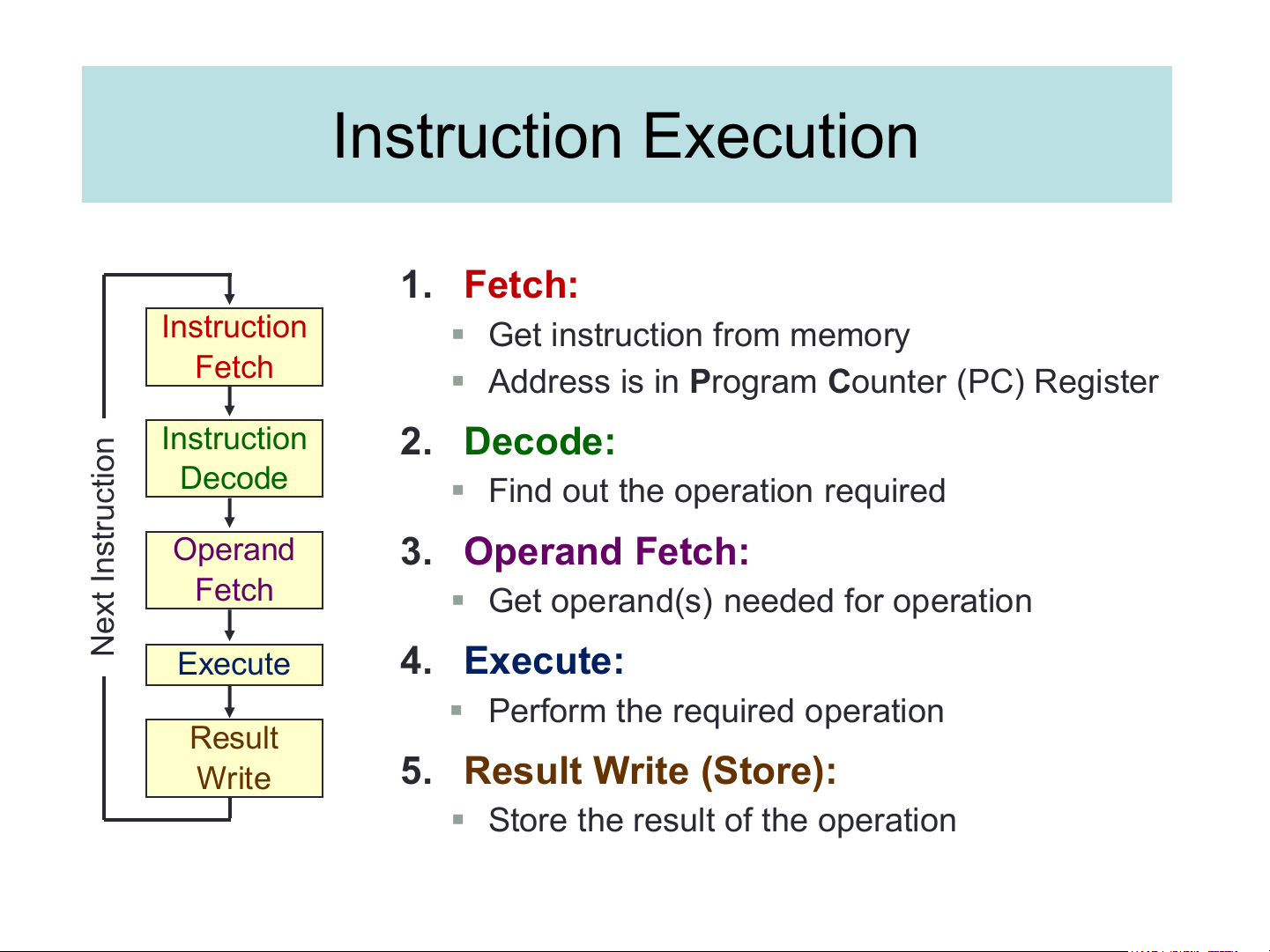
➢ Arithmetic/logical: add, sub, and, or, slt ➢ Control transfer: beq, j Instruction Execution 1. Fetch: Instruction
▪ Get instruction from memory Fetch
▪ Address is in Program Counter (PC) Register n Instruction 2. Decode: Decode ctio
▪ Find out the operation required Operand 3. Operand Fetch: Instru t Fetch x
▪ Get operand(s) needed for operation Ne Execute 4. Execute:
▪ Perform the required operation Result Write
5. Result Write (Store):
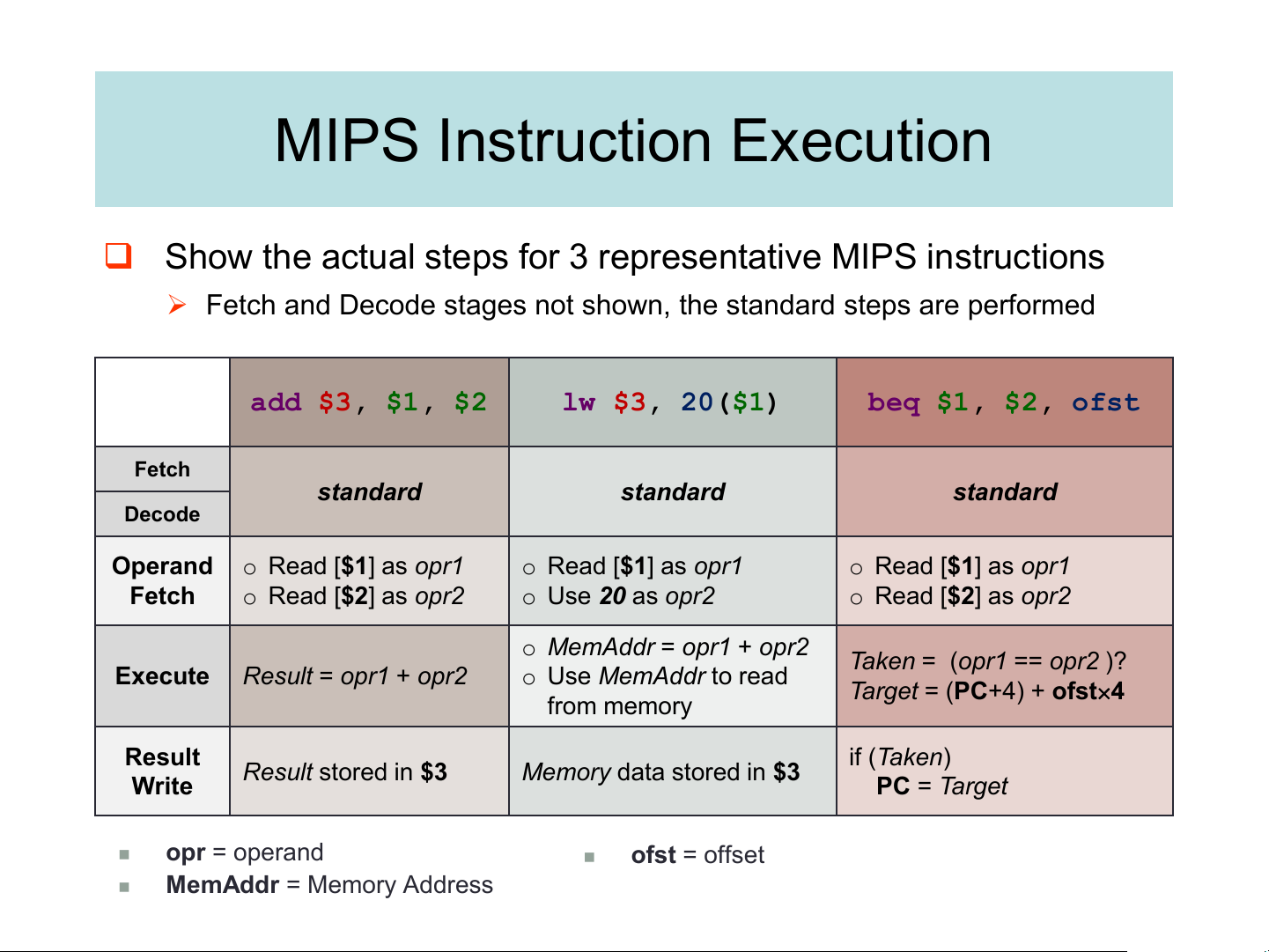
▪ Store the result of the operation MIPS Instruction Execution
❑ Show the actual steps for 3 representative MIPS instructions
➢ Fetch and Decode stages not shown, the standard steps are performed add $3, $1, $2 lw $3, 20($1) beq $1, $2, ofst Fetch standard standard standard Decode
Operand o Read [$1] as opr1
o Read [$1] as opr1
o Read [$1] as opr1 Fetch
o Read [$2] as opr2
o Use 20 as opr2
o Read [$2] as opr2
o MemAddr = opr1 + opr2
Taken = (opr1 == opr2 )? Execute
Result = opr1 + opr2 o Use MemAddr to read
Target = (PC+4) + ofst4 from memory Result if (Taken)
Result stored in $3
Memory data stored in $3 Write PC = Target ◼ opr = operand ◼ ofst = offset ◼
MemAddr = Memory Address
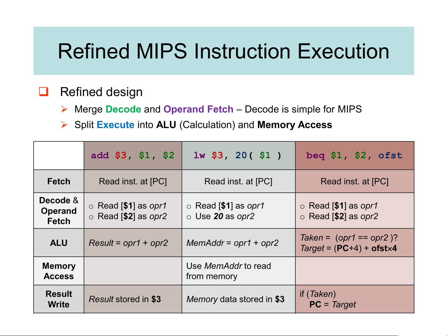
Refined MIPS Instruction Execution ❑ Refined design
➢ Merge Decode and Operand Fetch – Decode is simple for MIPS
➢ Split Execute into ALU (Calculation) and Memory Access add $3, $1, $2 lw $3, 20( $1 ) beq $1, $2, ofst Fetch Read inst. at [PC] Read inst. at [PC] Read inst. at [PC] Decode &
o Read [$1] as opr1
o Read [$1] as opr1
o Read [$1] as opr1 Operand
o Read [$2] as opr2
o Use 20 as opr2
o Read [$2] as opr2 Fetch
Taken = (opr1 == opr2 )? ALU
Result = opr1 + opr2
MemAddr = opr1 + opr2
Target = (PC+4) + ofst4 Memory Use MemAddr to read Access from memory Result if (Taken)
Result stored in $3
Memory data stored in $3 Write PC = Target Building MIPS datapath
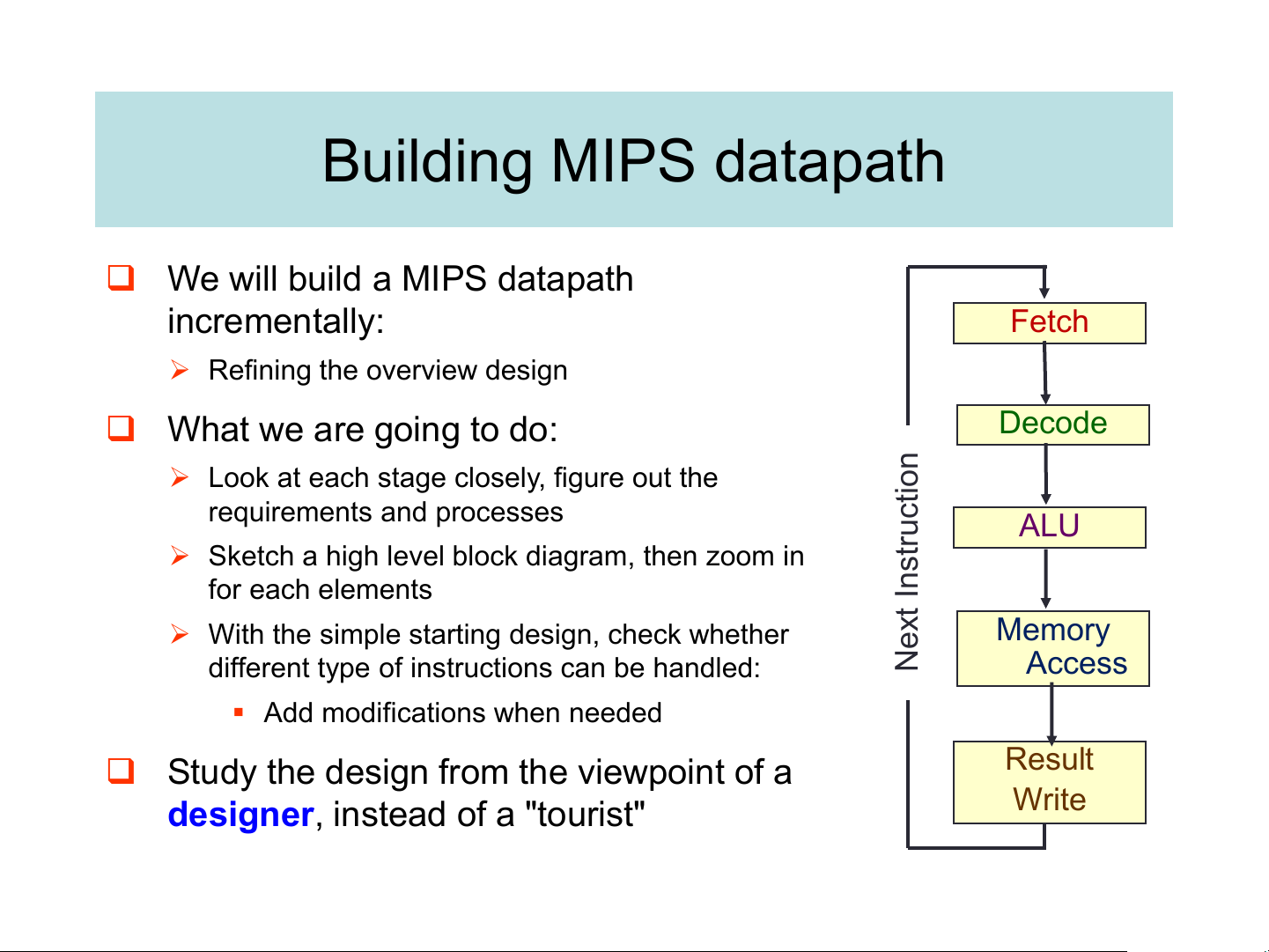
❑ We will build a MIPS datapath incrementally: Fetch
➢ Refining the overview design ❑ What we are going to do: Decode n
➢ Look at each stage closely, figure out the requirements and processes ALU
➢ Sketch a high level block diagram, then zoom in for each elements Instructio t
➢ With the simple starting design, check whether x Memory
different type of instructions can be handled: Ne Access
▪ Add modifications when needed
❑ Study the design from the viewpoint of a Result
designer, instead of a "tourist" Write Fetch Stage: Requirements
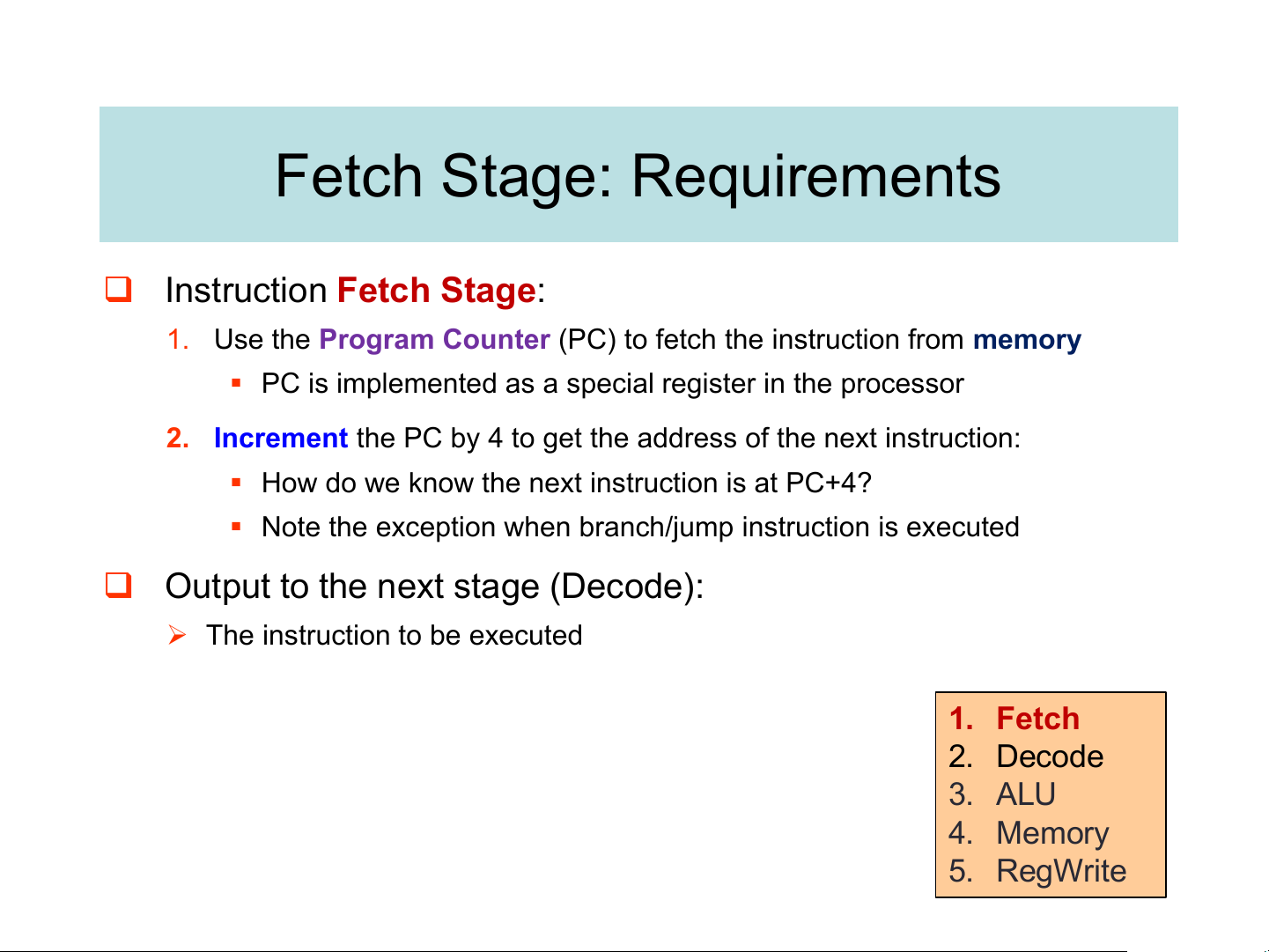
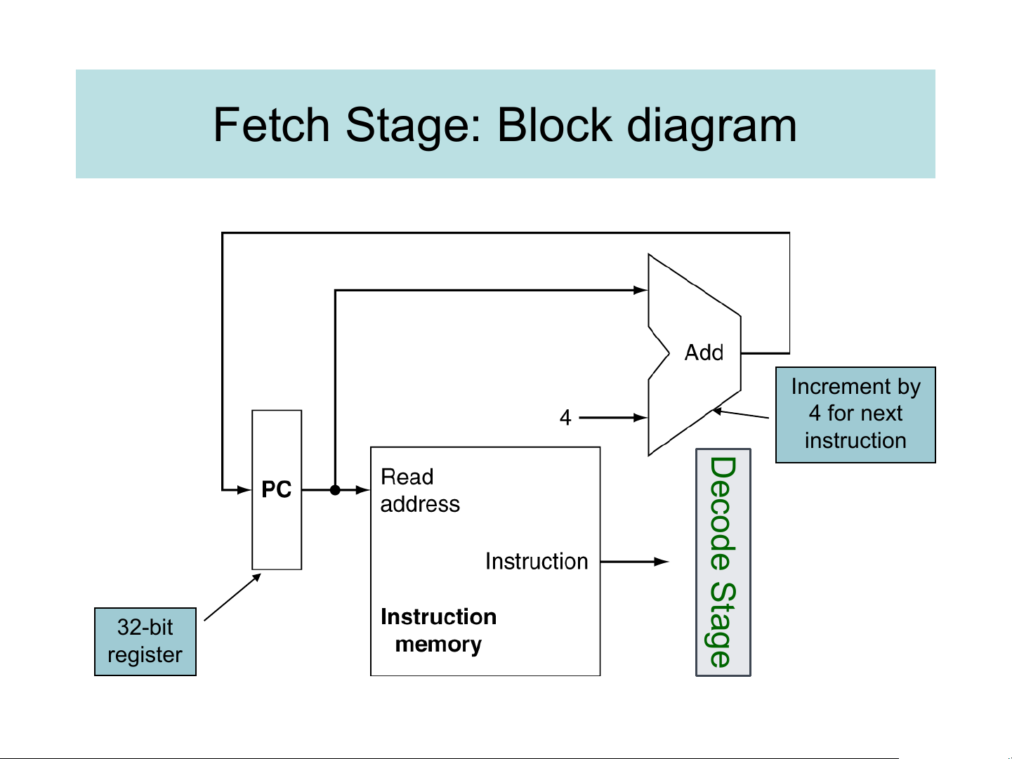
❑ Instruction Fetch Stage:
1. Use the Program Counter (PC) to fetch the instruction from memory
▪ PC is implemented as a special register in the processor
2. Increment the PC by 4 to get the address of the next instruction:
▪ How do we know the next instruction is at PC+4?
▪ Note the exception when branch/jump instruction is executed
❑ Output to the next stage (Decode):
➢ The instruction to be executed 1. Fetch 2. Decode 3. ALU 4. Memory 5. RegWrite Fetch Stage: Block diagram Increment by 4 for next instruction Decode Stage 32-bit register Element: Instruction Memory
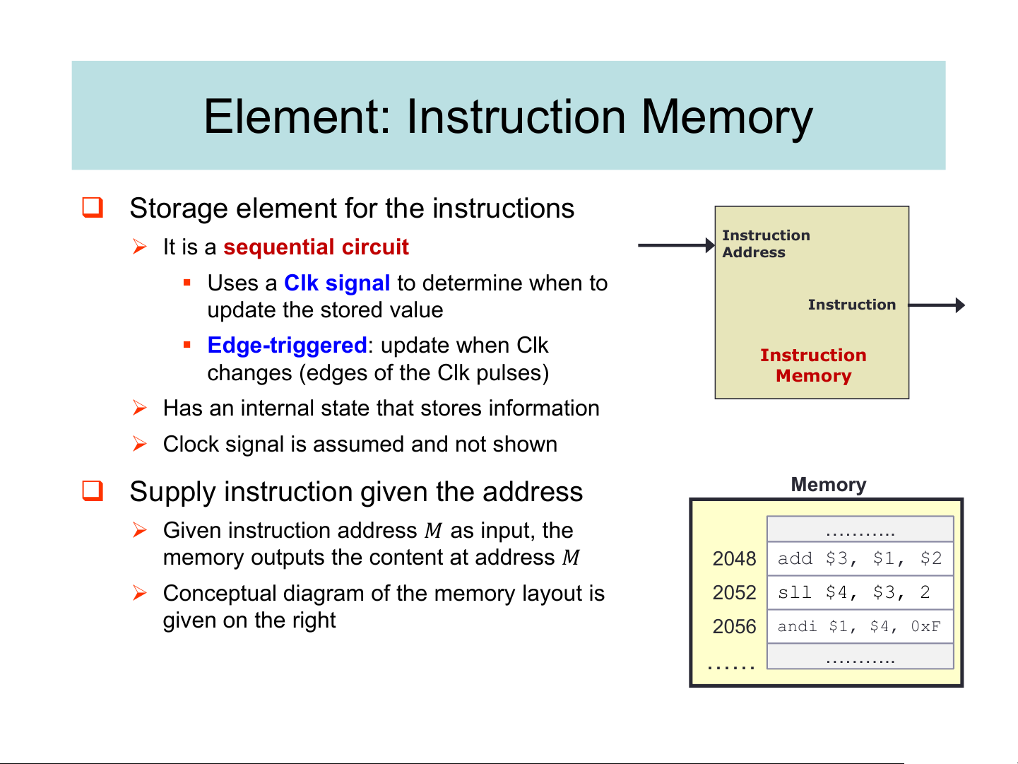
❑ Storage element for the instructions Instruction
➢ It is a sequential circuit Address
▪ Uses a Clk signal to determine when to Instruction update the stored value
▪ Edge-triggered: update when Clk Instruction
changes (edges of the Clk pulses) Memory
➢ Has an internal state that stores information
➢ Clock signal is assumed and not shown Memory
❑ Supply instruction given the address
➢ Given instruction address 𝑀 as input, the ………..
memory outputs the content at address 𝑀 2048 add $3, $1, $2
➢ Conceptual diagram of the memory layout is 2052 sll $4, $3, 2 given on the right 2056 andi $1, $4, 0xF …… ……….. The Idea of Clocking
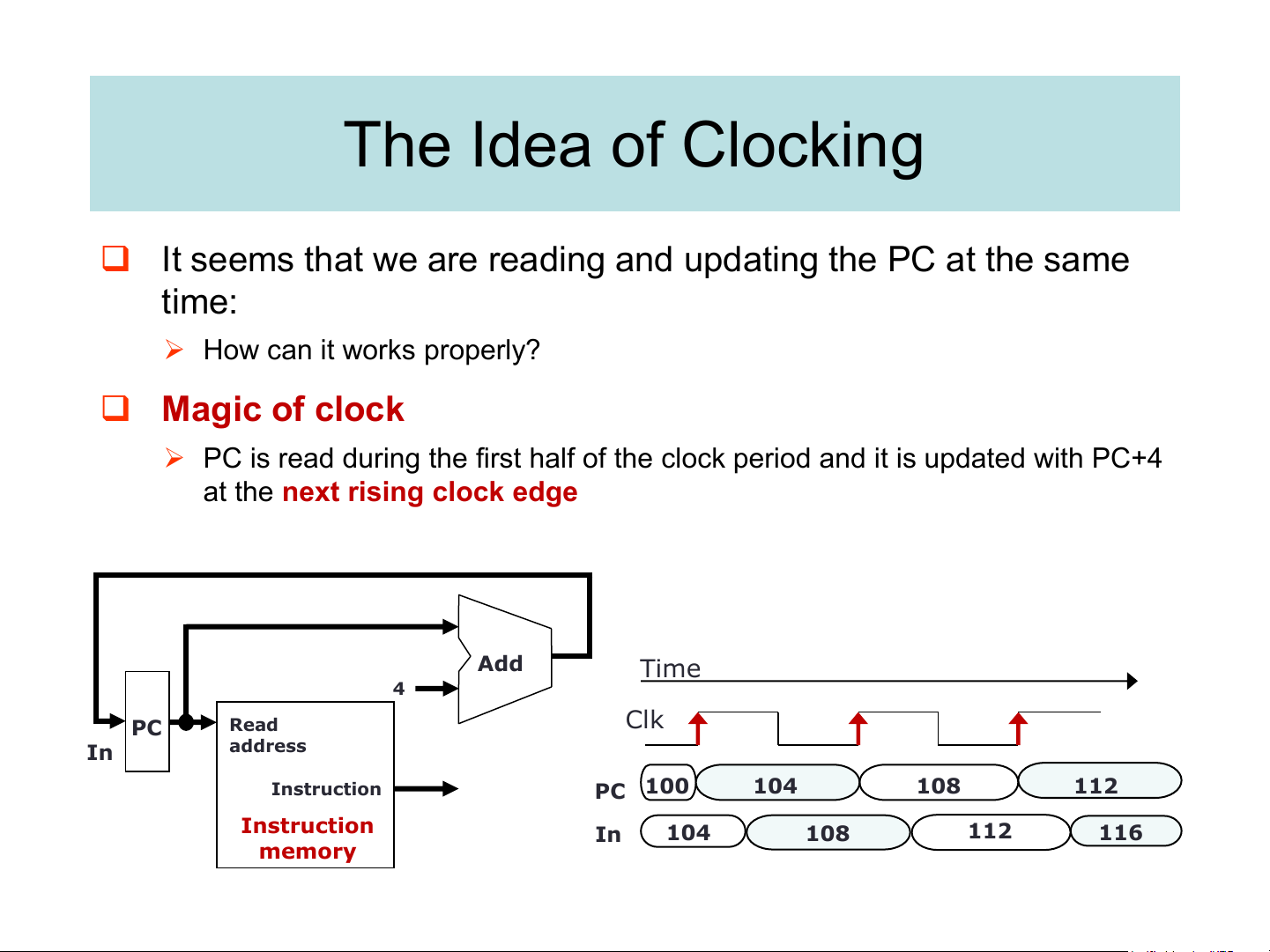
❑ It seems that we are reading and updating the PC at the same time: ➢ How can it works properly? ❑ Magic of clock
➢ PC is read during the first half of the clock period and it is updated with PC+4
at the next rising clock edge Add Time 4 PC Read Clk address In Instruction PC 100 104 108 112 Instruction In 104 108 112 116 memory Decode Stage: Requirements
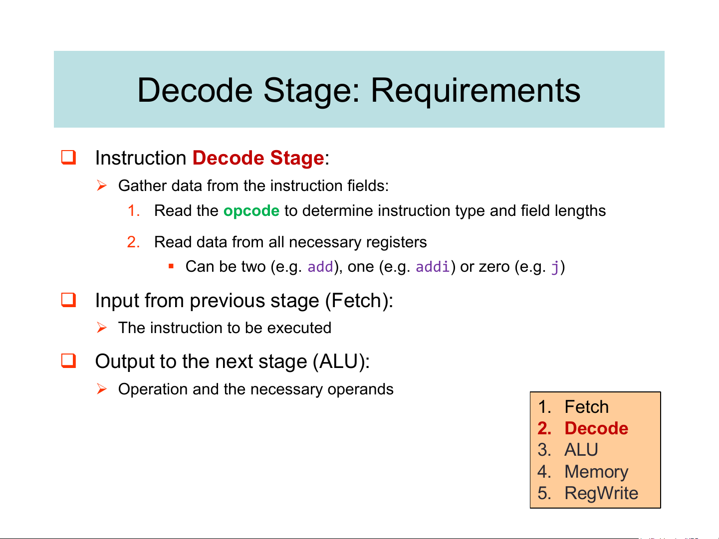
❑ Instruction Decode Stage:
➢ Gather data from the instruction fields:
1. Read the opcode to determine instruction type and field lengths
2. Read data from all necessary registers
▪ Can be two (e.g. add), one (e.g. addi) or zero (e.g. j)
❑ Input from previous stage (Fetch):
➢ The instruction to be executed
❑ Output to the next stage (ALU):
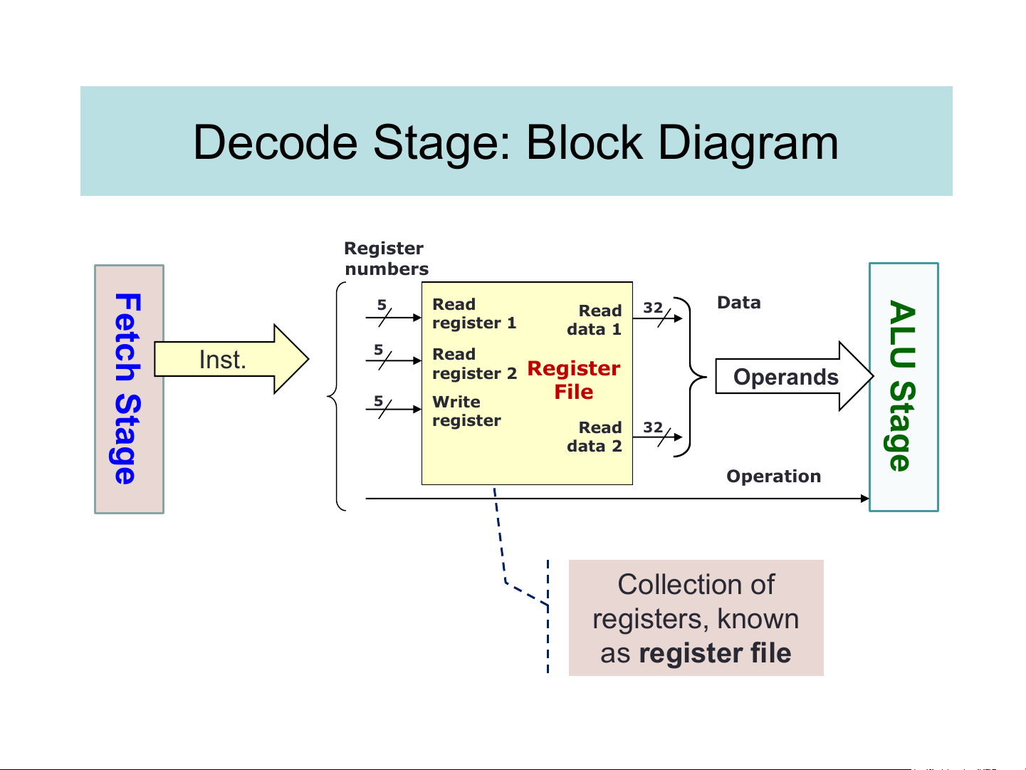
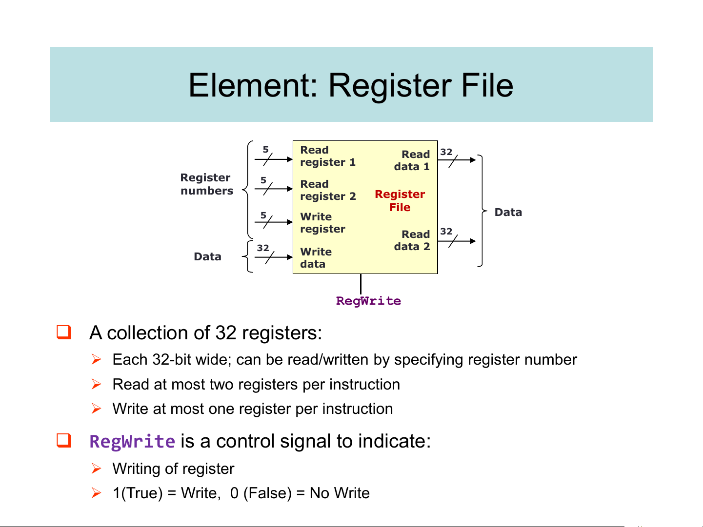
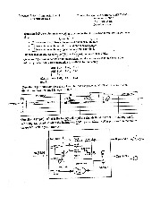
➢ Operation and the necessary operands 1. Fetch 2. Decode 3. ALU 4. Memory 5. RegWrite Decode Stage: Block Diagram Register Fetch Stage numbers AL 5 Read Data Read 32 register 1 data 1 U Inst. 5 Read register 2 Register Operands Stag File 5 Write register Read 32 data 2 e Operation Collection of registers, known as register file Element: Register File 5 Read Read 32 register 1 data 1 Register 5 Read numbers register 2 Register File 5 Write Data register 32 Read 32 data 2 Write Data data RegWrite
❑ A collection of 32 registers:
➢ Each 32-bit wide; can be read/written by specifying register number
➢ Read at most two registers per instruction
➢ Write at most one register per instruction
❑ RegWrite is a control signal to indicate: ➢ Writing of register
➢ 1(True) = Write, 0 (False) = No Write
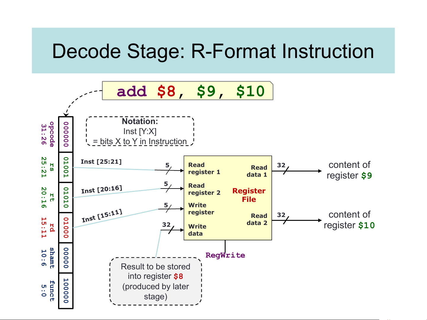
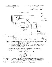
Decode Stage: R-Format Instruction add $8, $9, $10 opc 31: 000 Notation: ode 26 000 Inst [Y:X] = bits X to Y in Instruction 25: 010 rs Inst [25:21] 21 01 5 Read Read 32 content of register 1 data 1 register $9 20: 010 5 Read rt register 2 Register 16 10 File 5 Write 15: 010 register Read 32 content of rd data 2 11 00 32 Write register $10 data sha 10: 000 mt RegWrite 6 00 Result to be stored fun 100 into register $8 5:0 (produced by later ct 000 stage)
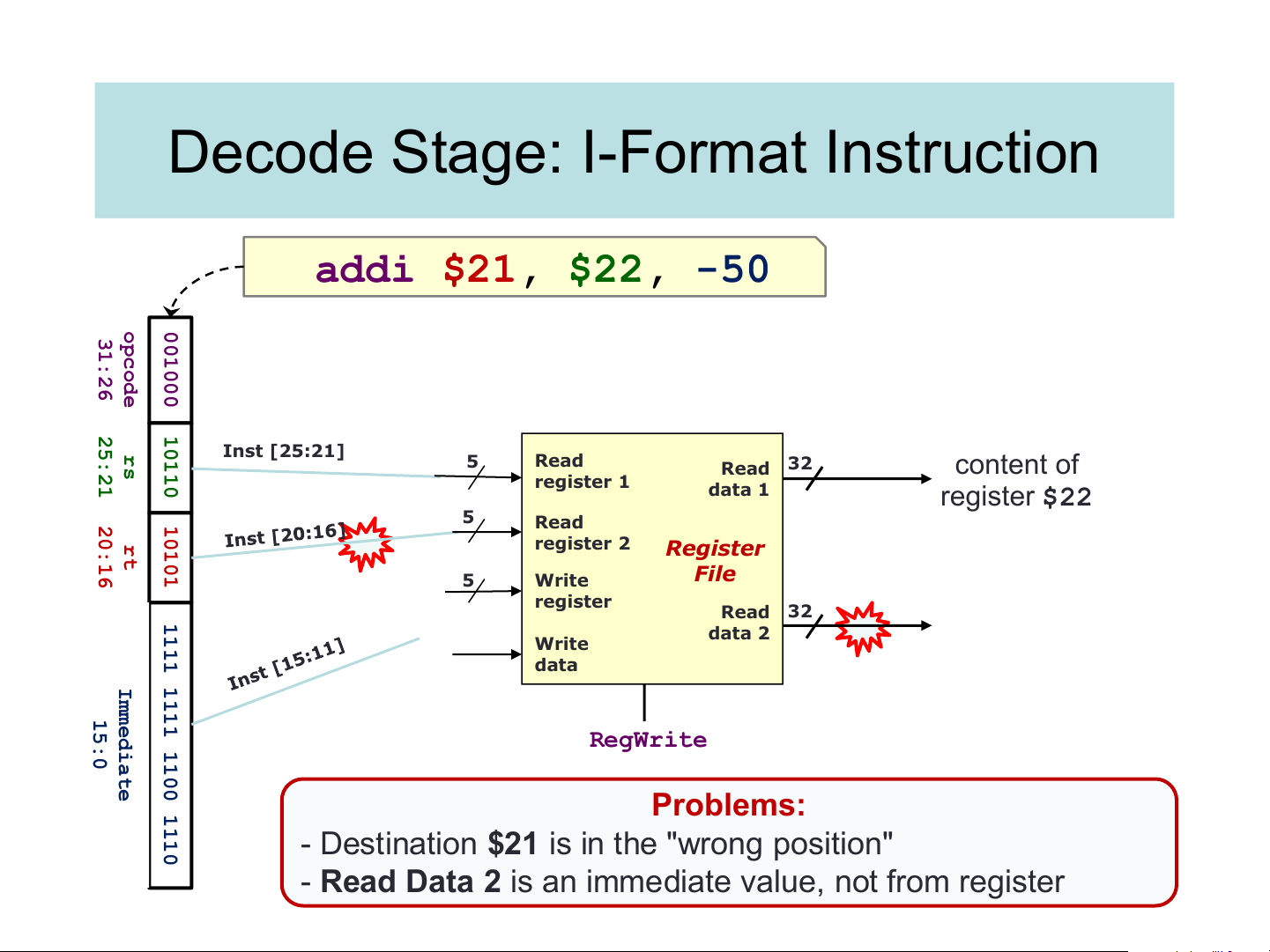
Decode Stage: I-Format Instruction addi $21, $22, -50 op 00 31: c 1 od 00 26 e 0 25: 101 rs Inst [25:21] 21 10 5 Read Read 32 content of register 1 data 1 register $22 20: 101 5 Read rt register 2 16 01 Register 5 Write File register 111 Read 32 data 2 Write 1 1 data Imm 11 15: edi 1 110 RegWrite 0 at e 0 1 Problems: 110
- Destination $21 is in the "wrong position"
- Read Data 2 is an immediate value, not from register
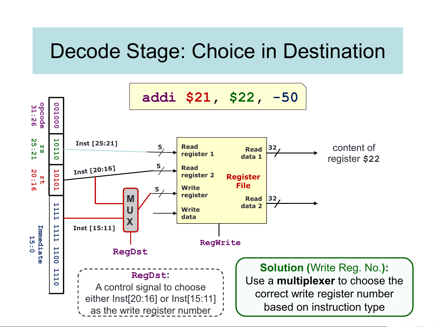
Decode Stage: Choice in Destination opc 001 addi $21, $22, -50 31: ode 000 26 25: 101 rs Inst [25:21] 21 10 5 Read Read 32 content of register 1 data 1 register $22 20: 101 5 Read rt register 2 16 01 Register Write File 5 register 111 M Read 32 data 2 Write 1 1 U data Imm X 11 Inst [15:11] 15: edi 1 110 RegWrite 0 at RegDst e 0 1 110
Solution (Write Reg. No.): RegDst:
Use a multiplexer to choose the A control signal to choose correct write register number
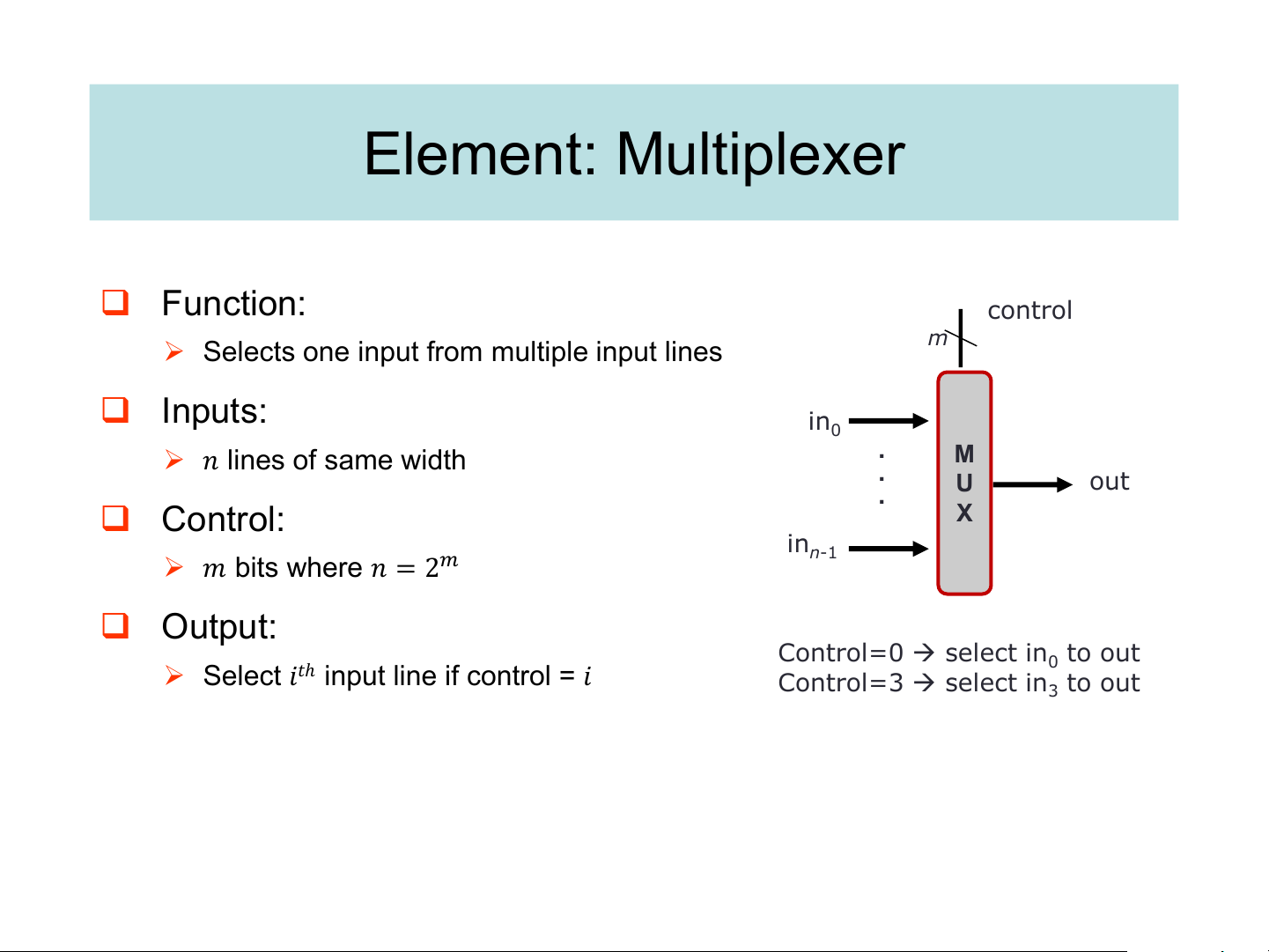
either Inst[20:16] or Inst[15:11] as the write register number based on instruction type Element: Multiplexer ❑ Function: control
➢ Selects one input from multiple input lines m ❑ Inputs: in0 ➢ 𝑛 lines of same width . M . U out . ❑ Control: X in ➢ 𝑚 n-1 bits where 𝑛 = 2𝑚 ❑ Output: Control=0 → select in to out ➢ 0
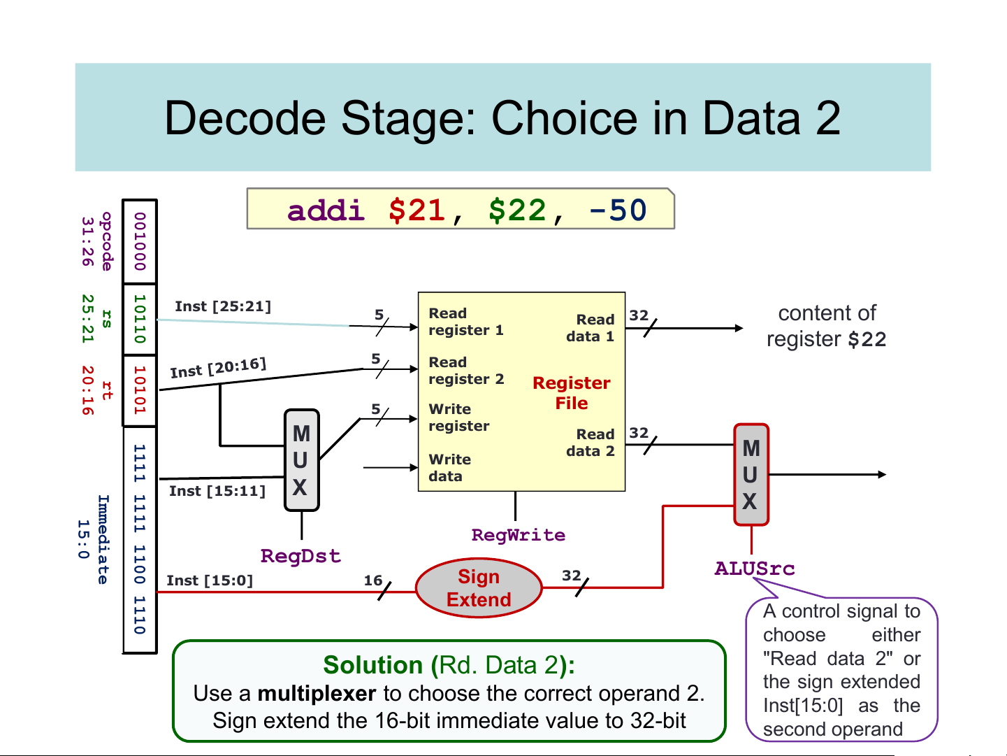
Select 𝑖𝑡ℎ input line if control = 𝑖 Control=3 → select in to out 3 Decode Stage: Choice in Data 2 opc 001 31: addi $21, $22, -50 ode 000 26 25: 101 rs Inst [25:21] 21 10 5 Read Read 32 content of register 1 data 1 register $22 20: 101 5 Read rt register 2 16 01 Register 5 Write File register 111 M Read 32 data 2 M Write 1 1 U data U Imm Inst [15:11] X 11 X 15: edi 1 110 RegWrite 0 at RegDst e 0 ALUSrc Inst [15:0] 16 Sign 32 1 110 Extend A control signal to choose either
Solution (Rd. Data 2): "Read data 2" or the sign extended
Use a multiplexer to choose the correct operand 2. Inst[15:0] as the
Sign extend the 16-bit immediate value to 32-bit second operand
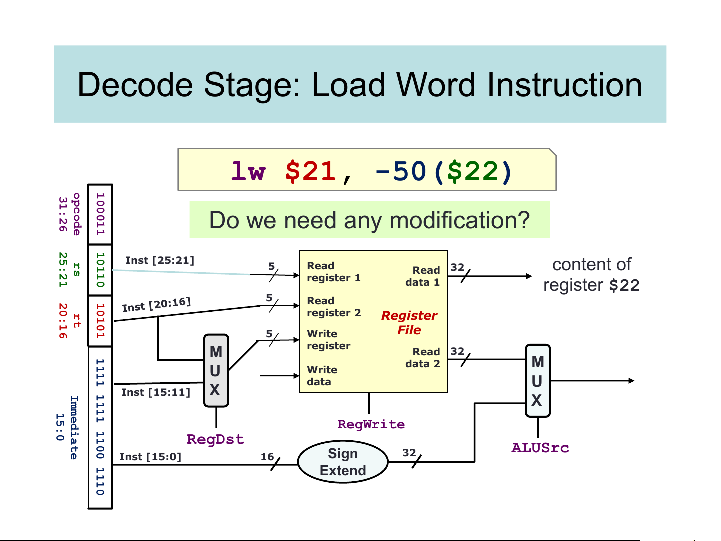
Decode Stage: Load Word Instruction lw $21, -50($22) opc 100 31: ode 011 26 Do we need any modification? 25: 101 rs Inst [25:21] 21 10 5 Read content of Read 32 register 1 data 1 register $22 20: 101 5 Read rt register 2 16 01 Register 5 Write File register 111 M Read 32 data 2 M Write 1 1 U data U Imm Inst [15:11] X 11 X 15: edi 1 110 RegWrite 0 at RegDst e 0 ALUSrc Inst [15:0] 16 Sign 32 1 110 Extend
Tài liệu liên quan:
-
TỔNG HỢP ĐỀ THI KTMT
24 12 -
Đề thi Kiến trúc máy tính đề số 2 năm học 2020-2021 | Trường Đại học Công nghệ, Đại học Quốc gia Hà Nội
213 107 -
Đề thi và đáp án Kiến trúc máy tính giữa kỳ 1 năm học 2021-2022 | Trường Đại học Công nghệ, Đại học Quốc gia Hà Nội
220 110 -
Đề thi Kiến trúc máy tính CLC giữa kỳ 1 năm học 2022-2023 | Trường Đại học Công nghệ, Đại học Quốc gia Hà Nội
179 90 -
Đề thi Kiến trúc máy tính CLC lần 2 giữa kỳ 1 năm học 2022-2023 | Trường Đại học Công nghệ, Đại học Quốc gia Hà Nội
138 69