SLIDE Week 8 – Lecture 8 – Single Cycle Processor Design (cont) Kiến Trúc Máy Tính | Trường Đại học Công nghệ, Đại học Quốc gia Hà Nội
SLIDE Week 8 – Lecture 8 – Single Cycle Processor Design (cont) Kiến Trúc Máy Tính | Trường Đại học Công nghệ, Đại học Quốc gia Hà Nội . Tài liệu được sưu tầm và biên soạn dưới dạng PDF gồm 23 trang giúp bạn tham khảo, củng cố kiến thức và ôn tập đạt kết quả cao trong kỳ thi sắp tới. Mời bạn đọc đón xem!
Môn: Kiến Trúc Máy Tính (UET) 19 tài liệu
Trường: Trường Đại học Công nghệ, Đại học Quốc gia Hà Nội 762 tài liệu
Tác giả:


Preview text:
ELT3047 Computer Architecture 4.4 in textbook
Lecture 8: Single Cycle Processor Design (cont.) Hoang Gia Hung
Faculty of Electronics and Telecommunications
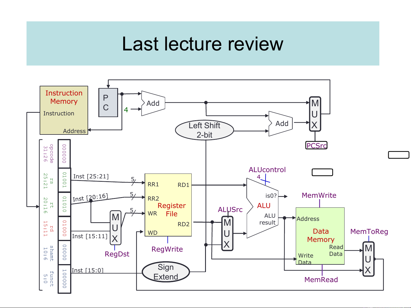
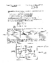
University of Engineering and Technology, VNU Hanoi Last lecture review Instruction P Memory Add M C 4 Instruction U Left Shift Add X Address 2-bit o 31:26 0 p 0
PCSrc tín hiệu điều khiển c 0 o 0 d 0 e 0 25:21 01001 ALUcontrol rs Inst [25:21] 5 4 RR1 RD1 20:16 01010 5 is0? MemWrite RR2 rt Register ALU 5 ALUSrc 15:11 01000 M WR File ALU Address rd RD2 M result U WD Data MemToReg Inst [15:11] U X Memory shamt 00000 10:6 X RegWrite Read M RegDst Data Write U Data funct 1 Sign 0 Inst [15:0] 5:0 X 0 0 Extend 0 MemRead 0
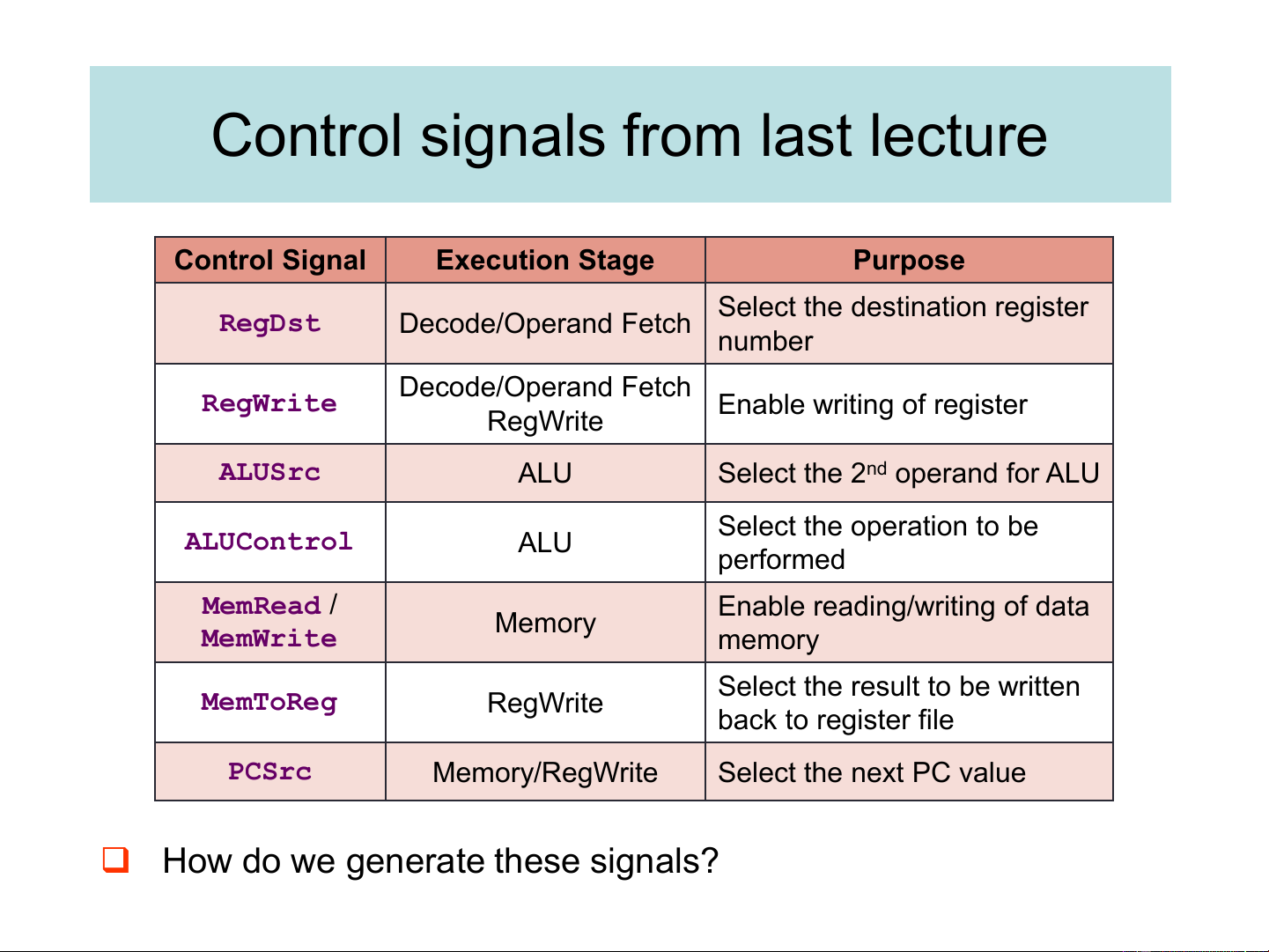
Control signals from last lecture Control Signal Execution Stage Purpose
Select the destination register lựa chọn toán RegDst Decode/Operand Fetch hạng là hằng number số hay nd t.ghi Decode/Operand Fetch cho phép ghi RegWrite Enable writing of register RegWrite dữ liệu hay k chọn operand ALUSrc ALU
Select the 2nd operand for ALU thứ 2 cho ALU Select the operation to be chọn operator ALUControl ALU performed MemRead /
Enable reading/writing of data Memory MemWrite memory chọn kết quả
Select the result to be written MemToReg RegWrite lấy ra từ registe back to register file hay alu PCSrc Memory/RegWrite Select the next PC value lựa chọn địa chỉ tiếp theo là PC + 4 hay ...
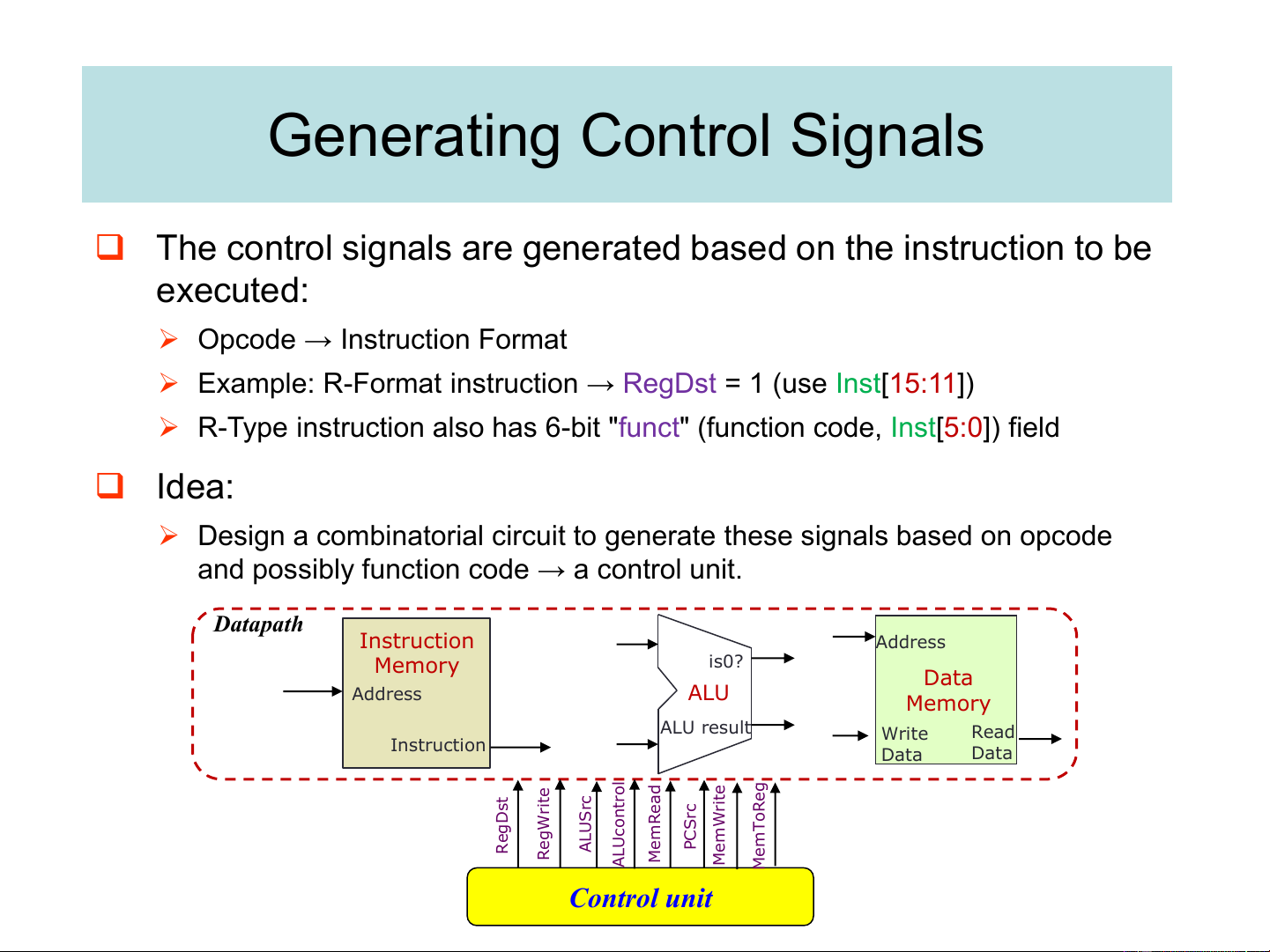
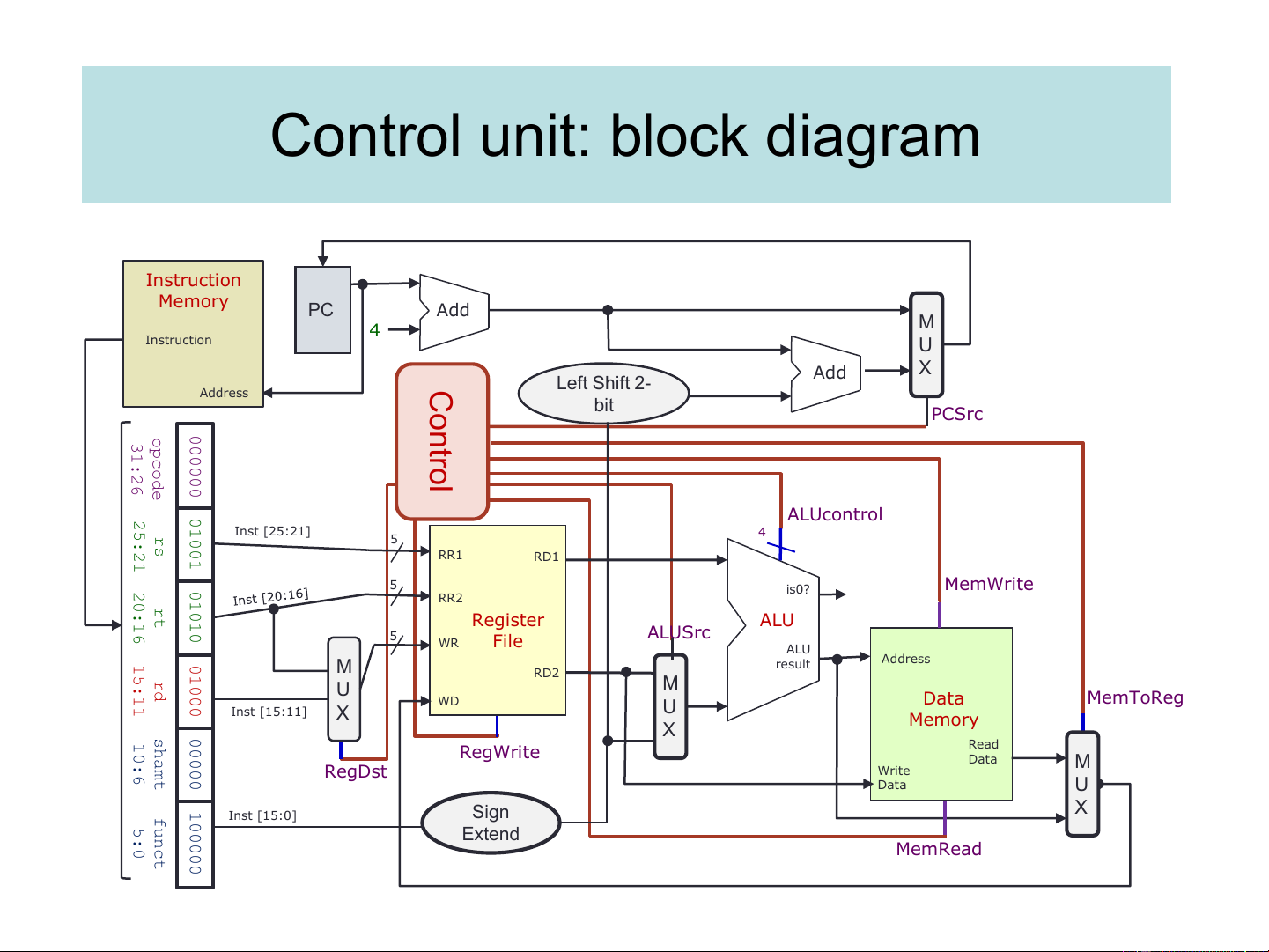
❑ How do we generate these signals? Generating Control Signals
❑ The control signals are generated based on the instruction to be executed:
➢ Opcode → Instruction Format
➢ Example: R-Format instruction → RegDst = 1 (use Inst[15:11])
➢ R-Type instruction also has 6-bit "funct" (function code, Inst[5:0]) field ❑ Idea:
➢ Design a combinatorial circuit to generate these signals based on opcode
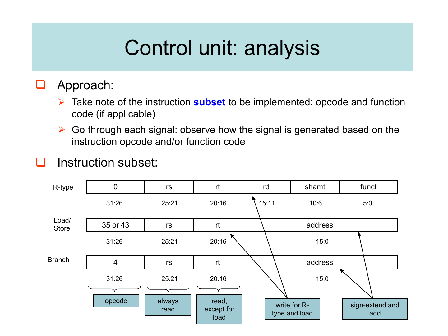
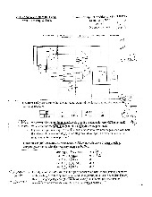
and possibly function code → a control unit. Datapath Instruction Address Memory is0? Data Address ALU Memory ALU result Write Read Instruction Data Data l e e t ro t t n rc Reg Dst Wri USrc co S L mRead U A e PC Reg mTo Reg e AL M MemWri M Control unit Control unit: block diagram Instruction Memory PC Add M 4 Instruction U Add X Co Left Shift 2- Address bit PCSrc n opcode 000000 31:26 trol 25:21 01001 ALUcontrol rs Inst [25:21] 4 5 RR1 RD1 5 20:16 01010 MemWrite is0? RR2 rt Register ALU 5 ALUSrc WR File ALU 15:11 01000 M result Address RD2 rd U M WD Data MemToReg Inst [15:11] X U Memory shamt 00000 X 10:6 RegWrite Read Data M Write RegDst Data U funct 100000 X Inst [15:0] Sign 5:0 Extend MemRead Control unit: analysis ❑ Approach:
➢ Take note of the instruction subset to be implemented: opcode and function
code (if applicable) xét từng loại lệnh một, để xm op và func là gì
➢ Go through each signal: observe how the signal is generated based on the
instruction opcode and/or function code ❑ Instruction subset: R-type 0 rs rt rd shamt funct 31:26 25:21 20:16 15:11 10:6 5:0 Load/ 35 or 43 rs rt address Store 31:26 25:21 20:16 15:0 Branch 4 rs rt address rẽ nhánh 31:26 25:21 20:16 15:0 opcode always read, write for R- sign-extend and read except for type and load add load
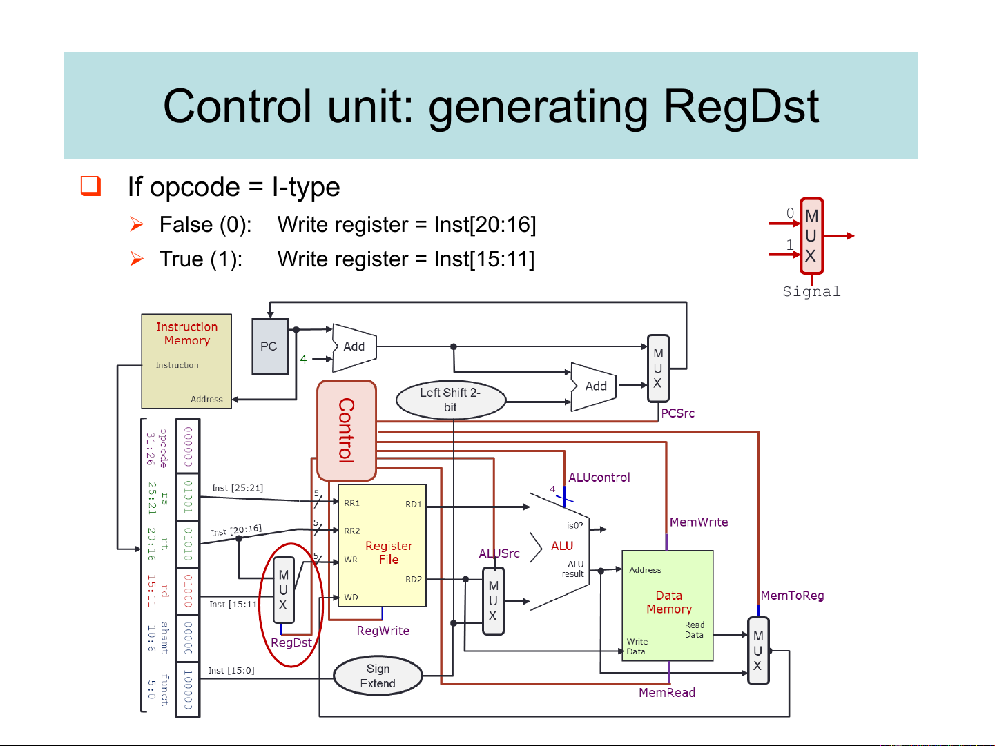
Control unit: generating RegDst ❑ If opcode = I-type ➢ 0 False (0): Write register = Inst[20:16] M U 1 ➢ True (1): Write register = Inst[15:11] X Signal
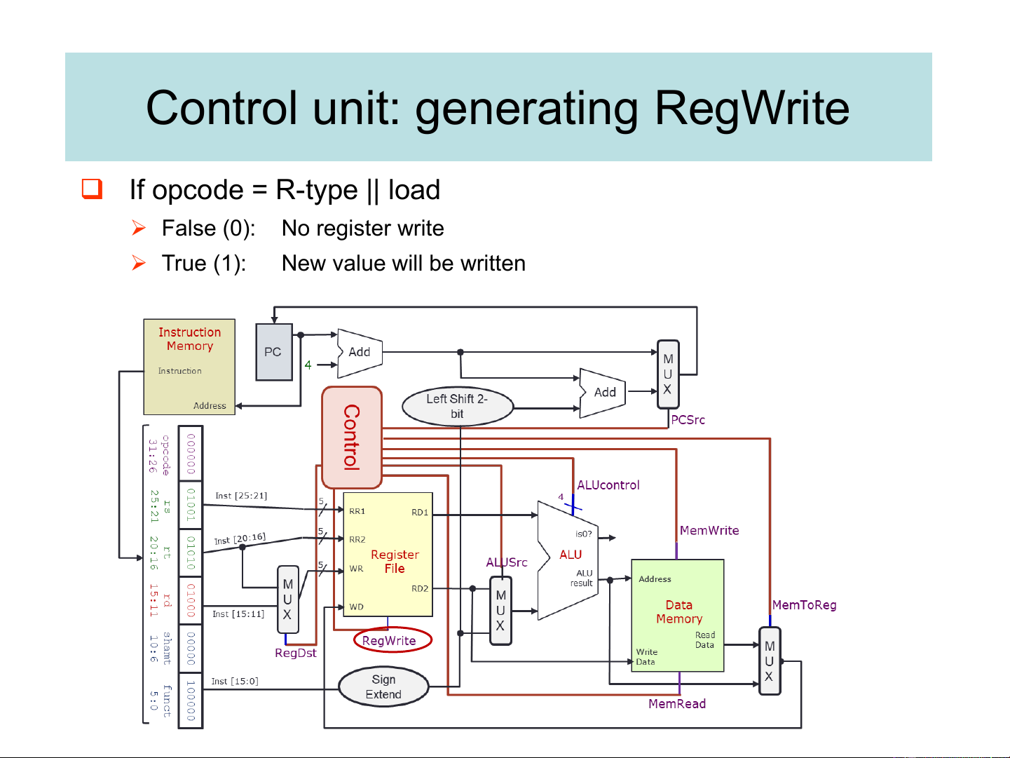
Control unit: generating RegWrite ❑ If opcode = R-type || load ➢ False (0): No register write ➢ True (1): New value will be written
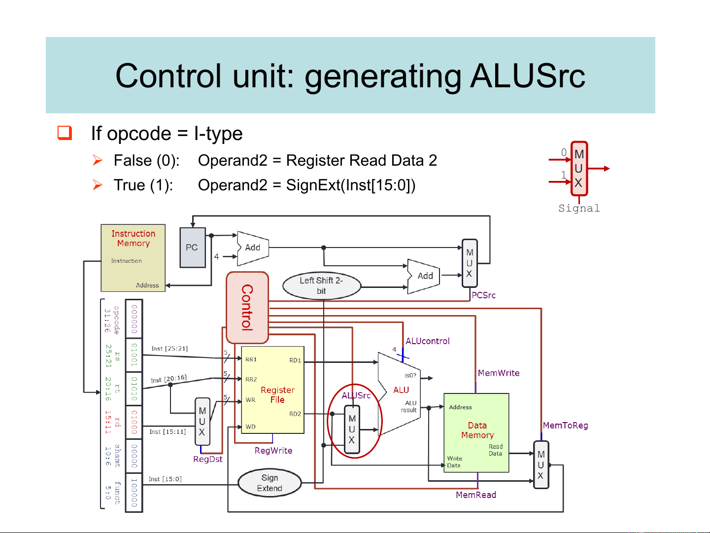
Control unit: generating ALUSrc ❑ If opcode = I-type 0 M ➢ False (0):
Operand2 = Register Read Data 2 U 1 X ➢ True (1): Operand2 = SignExt(Inst[15:0]) Signal
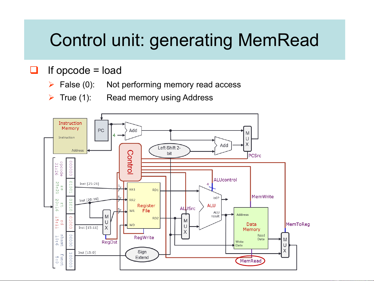
Control unit: generating MemRead ❑ If opcode = load ➢ False (0):
Not performing memory read access ➢ True (1): Read memory using Address
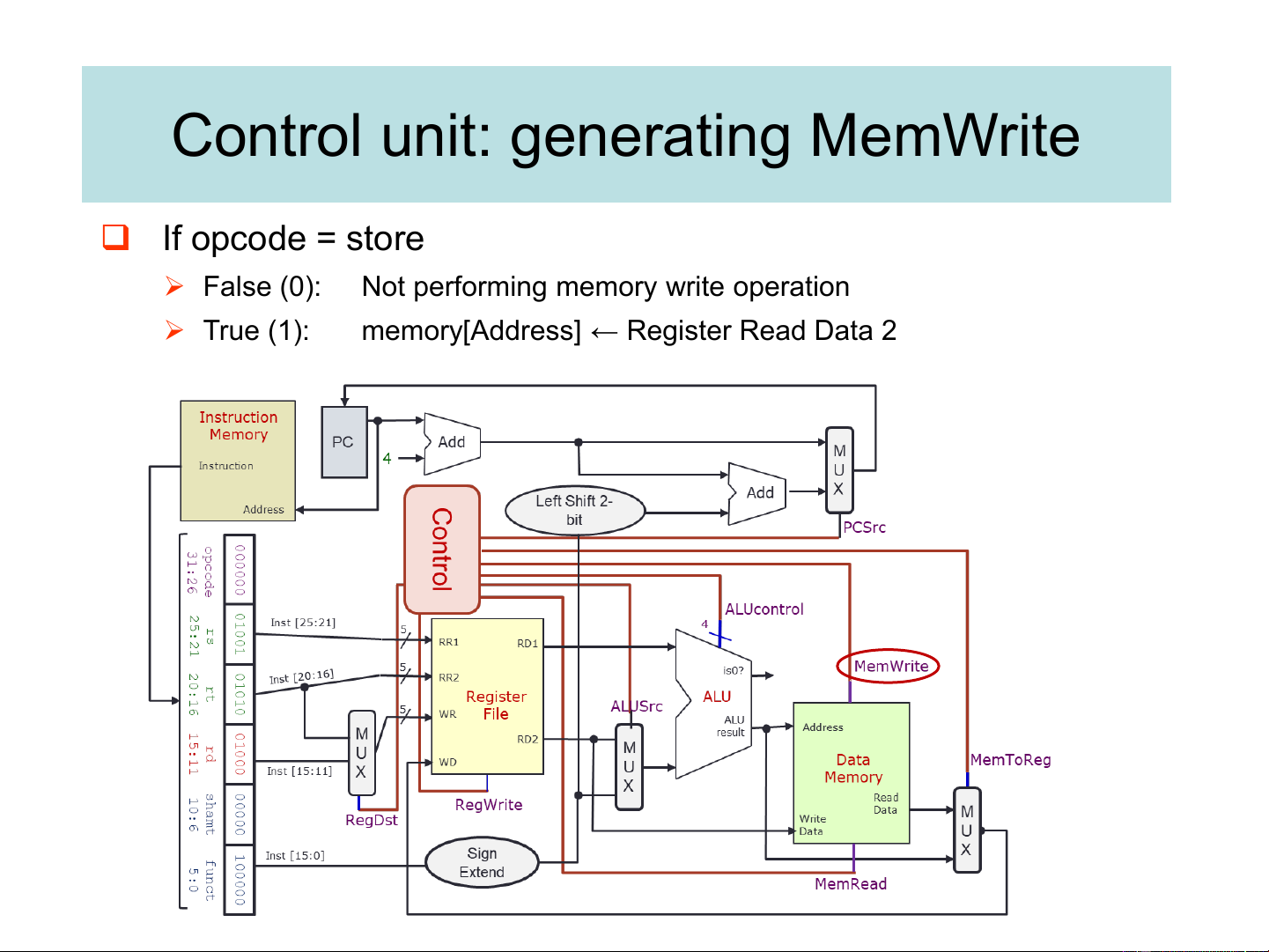
Control unit: generating MemWrite ❑ If opcode = store ➢ False (0):
Not performing memory write operation ➢ True (1):
memory[Address] ← Register Read Data 2
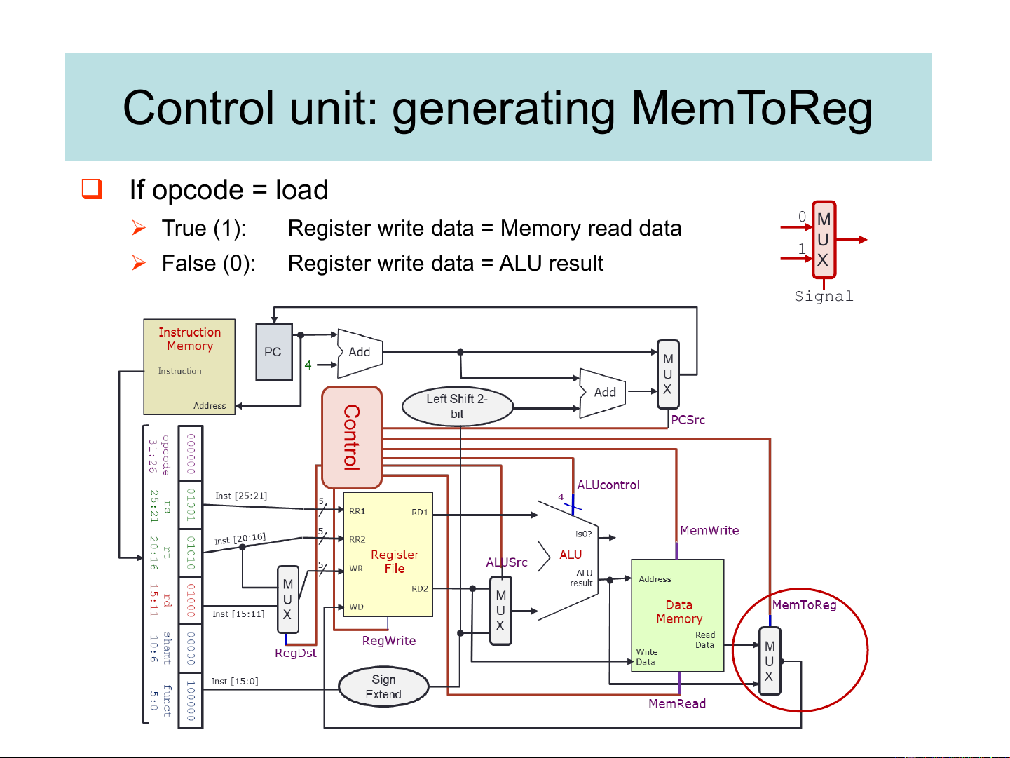
Control unit: generating MemToReg ❑ If opcode = load ➢ 0 True (1):
Register write data = Memory read data M U 1 ➢ False (0):
Register write data = ALU result X Signal Control unit: generating PCSrc
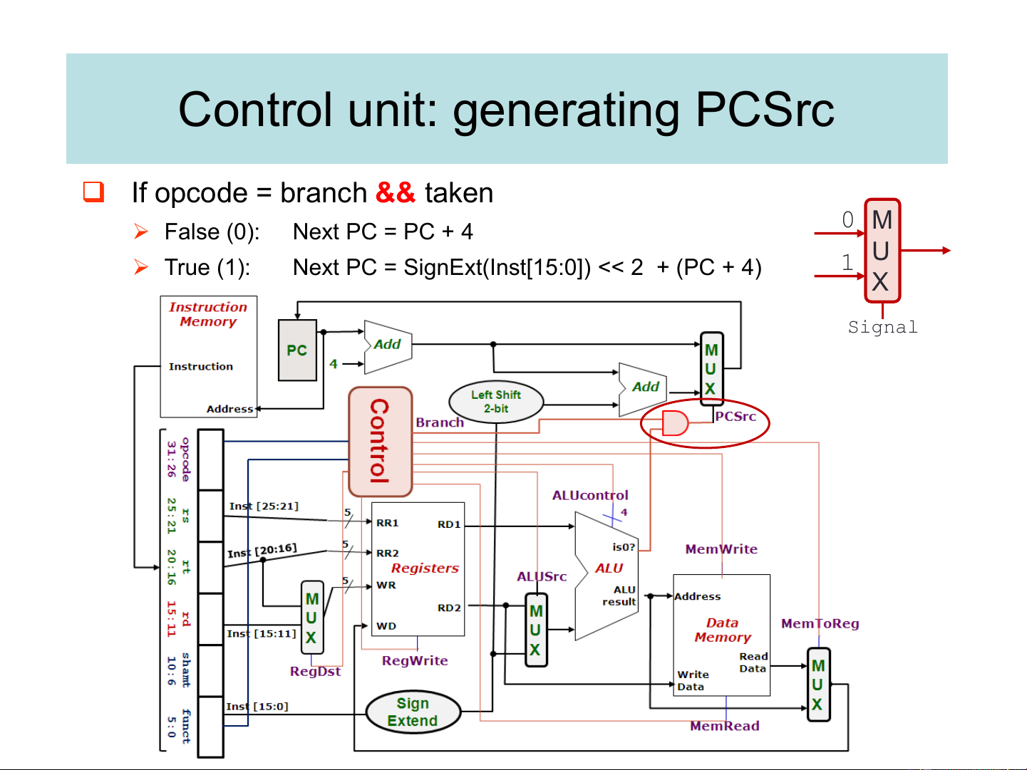
❑ If opcode = branch && taken ➢ 0 M False (0): Next PC = PC + 4 U ➢ True (1):
Next PC = SignExt(Inst[15:0]) << 2 + (PC + 4) 1 X Signal A closer look at ALU
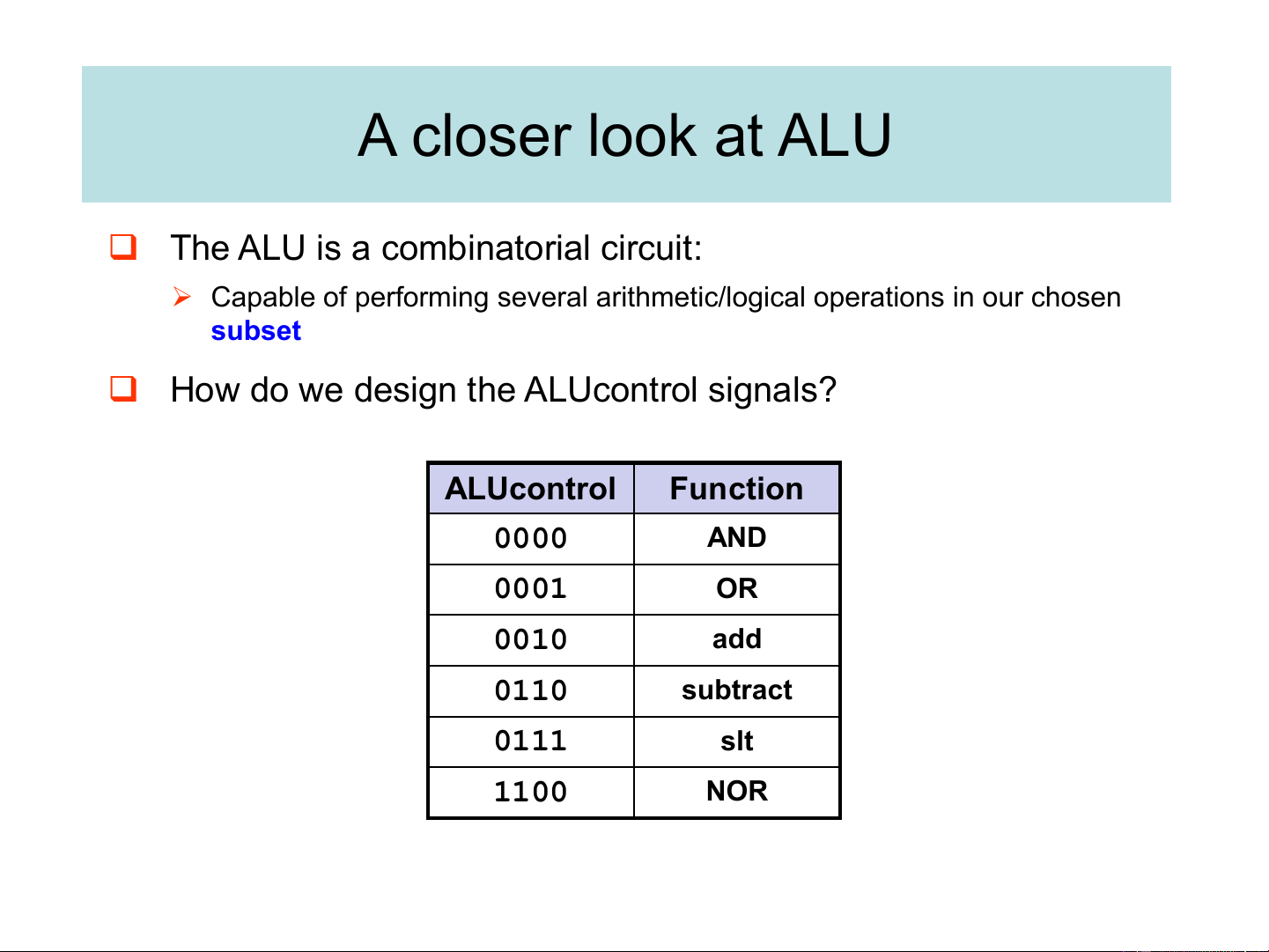
❑ The ALU is a combinatorial circuit:
➢ Capable of performing several arithmetic/logical operations in our chosen subset
❑ How do we design the ALUcontrol signals? ALUcontrol Function 0000 AND 0001 OR 0010 add 0110 subtract 0111 slt 1100 NOR ALU: One Bit At A Time
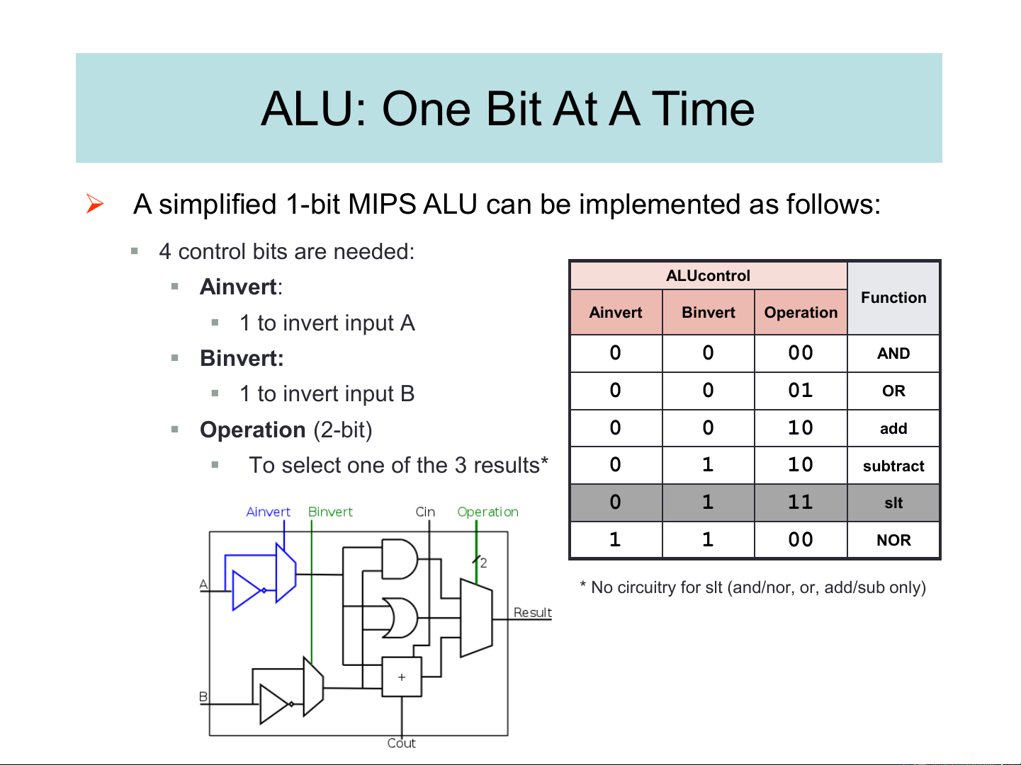
➢ A simplified 1-bit MIPS ALU can be implemented as follows: ▪ 4 control bits are needed: ▪ ALUcontrol Ainvert: Function ▪ Ainvert Binvert Operation 1 to invert input A ▪ Binvert: 0 0 00 AND ▪ 1 to invert input B 0 0 01 OR ▪ Operation (2-bit) 0 0 10 add ▪
To select one of the 3 results* 0 1 10 subtract 0 1 11 slt 1 1 00 NOR
* No circuitry for slt (and/nor, or, add/sub only) ALU: Two-level Implementation
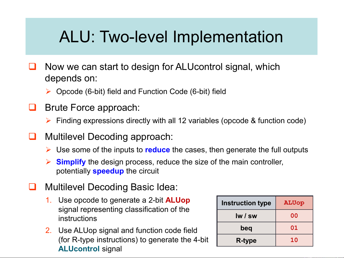
❑ Now we can start to design for ALUcontrol signal, which depends on:
➢ Opcode (6-bit) field and Function Code (6-bit) field ❑ Brute Force approach:
➢ Finding expressions directly with all 12 variables (opcode & function code)
❑ Multilevel Decoding approach:
➢ Use some of the inputs to reduce the cases, then generate the full outputs
➢ Simplify the design process, reduce the size of the main controller,
potentially speedup the circuit
❑ Multilevel Decoding Basic Idea:
1. Use opcode to generate a 2-bit ALUop Instruction type ALUop
signal representing classification of the lw / sw 00 instructions beq 01
2. Use ALUop signal and function code field
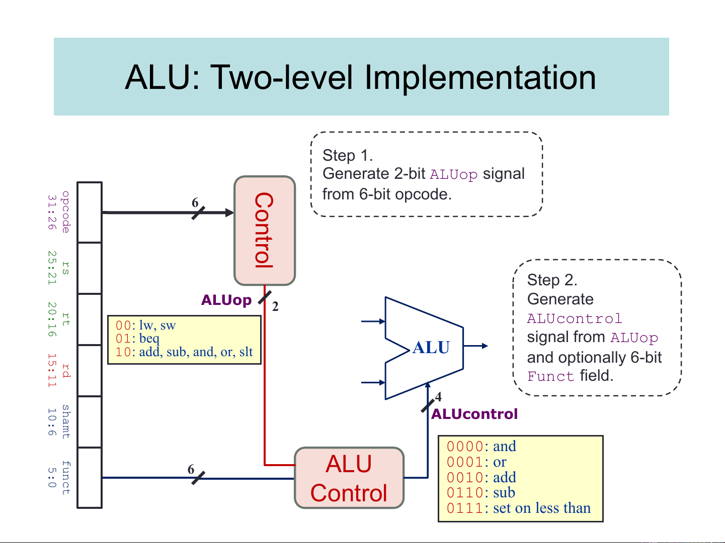
(for R-type instructions) to generate the 4-bit R-type 10 ALUcontrol signal ALU: Two-level Implementation Step 1. Generate 2-bit ALUop signal opc Co 31: from 6-bit opcode. 6 ode 26 ntr 25: ol rs 21 Step 2. 20: ALUop Generate rt 2 16 ALUcontrol 00: lw, sw 01: beq signal from ALUop 15: ALU 10: add, sub, and, or, slt rd and optionally 6-bit 11 Funct field. sha 4 10: ALUcontrol mt 6 0000: and fun 5:0 0001: or 6 ALU ct 0010: add Control 0110: sub 0111: set on less than
ALUcontrol & ALUop expected values Instruction Funct ALU ALU Opcode ALUop Operation field action control lw 00 load word xxxxxx add 0010 sw 00 store word xxxxxx add 0010 beq 01 branch equal xxxxxx subtract 0110 R-type 10 add 10 0000 add 0010 R-type 10 subtract 10 0010 subtract 0110 R-type 10 AND 10 0100 AND 0000 R-type 10 OR 10 0101 OR 0001 set on less set on R-type 10 10 1010 0111 than less than
Generation of 4-bit ALUcontrol will be discussed first,
that of 2-bit ALUop signal will be discussed later
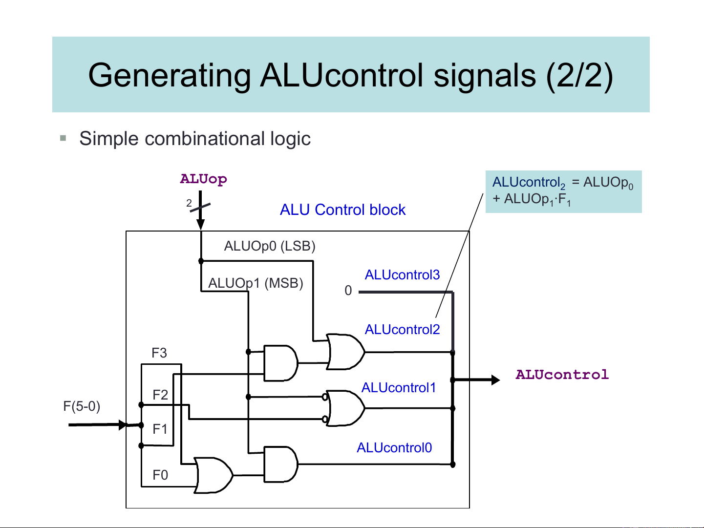
Generating ALUcontrol signals (1/2)
▪ Input: 6-bit Funct field and 2-bit ALUop ALUcontrol = 0 3
▪ Output: 4-bit ALUcontrol ALUcontrol = ? 2
▪ Find the simplified expressions
ALUop + ALUop F 0 1 1 thi có thể có Funct Field ALUop
( F[5:0] == Inst[5:0] ) ALU control MSB LSB F5 F4 F3 F2 F1 F0 lw 0 0 X X X X X X 0 0 1 0 sw 0 0 X X X X X X 0 0 1 0 beq 0 X 1 X X X X X X 0 1 1 0 add 1 0 X 1 X 0 X 0 0 0 0 0 0 1 0 sub 1 0 X 1 X 0 X 0 0 1 0 0 1 1 0 and 1 0 X 1 X 0 X 0 1 0 0 0 0 0 0 or 1 0 X 1 X 0 X 0 1 0 1 0 0 0 1 slt 1 0 X 1 X 0 X 1 0 1 0 0 1 1 1
Generating ALUcontrol signals (2/2) ▪ Simple combinational logic ALUop ALUcontrol = ALUOp 2 0 ∙F 2 + ALUOp ALU Control block 1 1 ALUOp0 (LSB) ALUcontrol3 ALUOp1 (MSB) 0 ALUcontrol2 F3 ALUcontrol ALUcontrol1 F2 F(5-0) F1 ALUcontrol0 F0
Tài liệu liên quan:
-
TỔNG HỢP ĐỀ THI KTMT
24 12 -
Đề thi Kiến trúc máy tính đề số 2 năm học 2020-2021 | Trường Đại học Công nghệ, Đại học Quốc gia Hà Nội
213 107 -
Đề thi và đáp án Kiến trúc máy tính giữa kỳ 1 năm học 2021-2022 | Trường Đại học Công nghệ, Đại học Quốc gia Hà Nội
220 110 -
Đề thi Kiến trúc máy tính CLC giữa kỳ 1 năm học 2022-2023 | Trường Đại học Công nghệ, Đại học Quốc gia Hà Nội
179 90 -
Đề thi Kiến trúc máy tính CLC lần 2 giữa kỳ 1 năm học 2022-2023 | Trường Đại học Công nghệ, Đại học Quốc gia Hà Nội
138 69