A Low Voltage Very High Impedance Current Mirror Circuit and Its Application
A Low Voltage Very High Impedance Current Mirror Circuit and Its Application. Tài liệu được sưu tầm giúp bạn tham khảo, ôn tập và đạt kết quả cao. Mời bạn đọc đón xem.
Môn: Tài liệu Tổng hợp 3.6 K tài liệu
Trường: Tài liệu khác 3.9 K tài liệu
Tác giả:

Preview text:
2013 International Conference on Control Communication and Computing (ICCC)
A Low Voltage Very High Impedance Current Mirror Circuit and Its Application Mrs.Priya M K Mrs.Vanitha Rugmoni V K
PG Scholar, VLSI & Embedded System, Dept. of ECE,
Asst. Professor, Dept. of ECE,
Viswajyothi College of Engineering, Vazhakulam
Viswajyothi College of Engineering, Vazhakulam, Ernakulam, India Ernakulam, India mkpriya457@gmail.com vanitharugmoni@gmail.com
Abstract—Current mirror circuit has served as the basic
output and voltage range. A feedback action is used to force
building block in analog circuit design since the introduction of
the input and output currents to be equal. The proposed
integrated circuits. In this paper, “A Very high impedance
circuit is also insensitive to the biasing current. This
current mirror, operating in reduced power supply which does
implementation yields an increase in the output impedance
not use any additional biasing circuit and its application” is by a factor of about g
proposed. The design uses a high swing super Wilson current
mro compared with that of the super-
mirror which has negative feedback. A feedback action is used
Wilson current mirror, thus offering a potential solution to
to force the input and output currents to be equal. The output
mitigate the effect of the low output impedance of deep
current is expected to be mirrored with a transfer error less
submicron CMOS transistors used in low voltage current
than 1% when the input current is increased from 5μA to 40μA.
mirrors and current sources. An NMOS version of the
As an application, the current mirror circuit has been used in
proposed current mirror circuit is aimed to be implemented
the design of a high gain, improved output swing differential
using CMOS process and simulated using SPICE to validate
amplifier. A telescopic differential amplifier is chosen for
its performance. The output current is expected to be
designing since it is used in low power application. A
mirrored with a transfer error lower than 1% when the input
comparative study of different current mirror circuits and
current is increased from 5μA to 40μA. The project is further
amplifier is also made. The output swing of the circuit is
improved than what is expected.
extended in designing an amplifier circuit using the proposed
current mirror circuit. A high performance Telescopic
Keywords—Current mirror, Wilson current mirror, Output
differential amplifier involving less power consumption,
Impedance, CMRR,Telescopic Differential Amplifier
high gain etc is designed. The Telescopic differential
amplifier has the inherent disadvantage of low output swing. I. INTRODUCTION
A high-swing, high performance single stage CMOS
Telescopic operational amplifier is analyzed and the results
In the early 1980s many experts predicted the demise of
are presented. The high swing of the op-amp is achieved by
analog circuits. Many functions that had been traditionally
employing the tail and current source transistors in the deep
realized in analog form were now easily performed in the
linear region. Also the tail current transistor is replaced by
digital domain, suggesting that with enough capability in IC
the current mirror circuit as a modified circuit.
fabrication all processing of signals would eventually occur
digitally. But still analog designers are of great demand
The paper is organised as follows, the section II describes
today. This is because there are many areas where it is very
the operation of the circuit. The simulation results are shown
difficult or even impossible to replace analog functions with
in section III and the conclusions are drawn in section IV.
their digital counterparts regardless of advancements in
Also the design specifications of current mirror and op-amp
technology. Digitization often requires analog blocks before
are tabularised. The simulation results are also tabularised. To
digitizing. A major component in these analog circuits is the
get a better understanding of the advantages of the proposed
current mirror, especially a high impedance current mirror in
current mirror circuit and the op-amp circuit, the comparative
the case of biomedical applications. The project aims at the
study the results is also made.
design of a current mirror circuit and its application in an
amplifier circuit. In this paper, “A very high impedance II. CIRCUIT OPERATION
current mirror, with less number of transistors which can
operate at low voltage without any additional biasing A. Basic Inspiration Circuits for the proposed current
circuitry” [1] is proposed. The fundamental design of this mirror circuit
circuit is a high-swing super-Wilson, which offers high
The basic inspirational circuits for the project are the
output impedance using negative feedback. The proposed
high swing super Wilson current mirror circuit[2],[3] ,the
current mirror uses MOS current dividers to sample the
improved high swing super Wilson Current mirror circuit [3]
output current to achieve very high impedance with a large
978-1-4799-0575-1/13/$31.00 ©2013 IEEE 511
and the high swing low voltage super Wilson Current Mirror
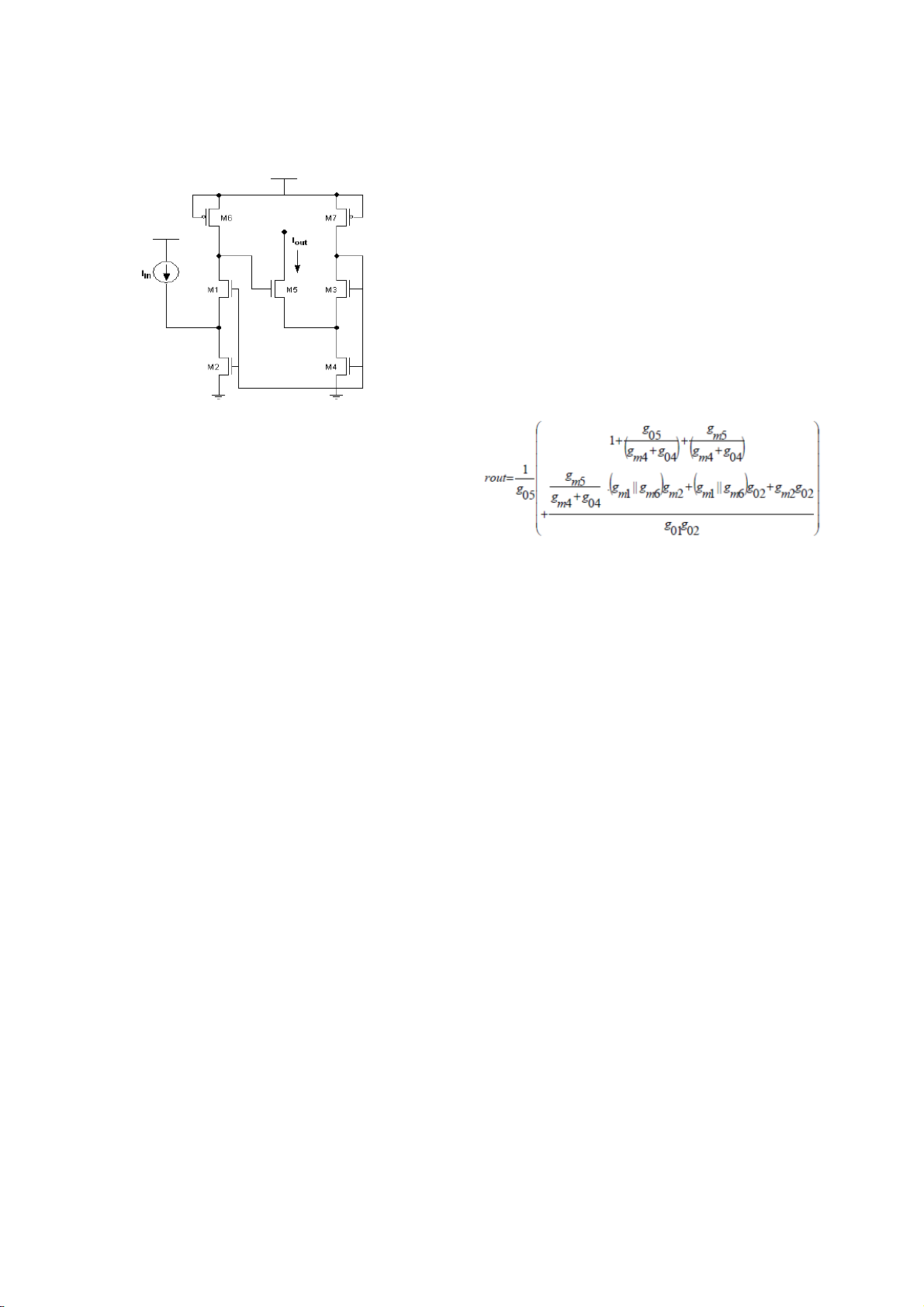
C. Auxiliary Current sources were needed for keeping
Circuit[1]. All these are high output impedance current drain symmetry.
mirror circuits. The high-swing super-Wilson CM [3] The new high output impedance current mirror in fig 1 is achieves a high
evolved from the Improved High swing Wilson current
mirror circuit described above to overcome these
disadvantages. The drain symmetry current mirror is
achieved without the need of an auxiliary current source. It is
achieved by replacing the auxiliary current source with the
PMOS. The M2-M4 transistors formed as part of the current
mirror are used to achieve high output impedance. The diode
connected transistor M1 is modified as a cascoded one. The
transistors M2-M4 samples the output current Iout and
compares it with the input current Iin which changes the
conduction of the transistor M5 and the output current Iout is
made equal to the input current Iin. The diode connected
transistors M6-M7 acts as an active load and increase the
output impedance as well as the output current. The
increased output impedance [1], [3] can be expressed as:
Fig.1. Low Voltage High Swing Super Wilson Current Mirror
output resistance by using negative feedback. Assuming that
the output resistance of the current sources is very large and
that transistors are saturated, the output resistance rout of the
high-swing super-Wilson CM [3] can be approximated as:
rout = gm2 ro2ro3 where gm2 and ro are respectively the
transconductance and the output resistance. In the high- (1)
swing super-Wilson CM discussed above, a diode-connected
where gm1, gm2, gm4, gm5 and go1, go2, go4, go5 are
transistor is used. It is to reduce current mismatch between
respectively the transconductance and the output
IIN and IOUT by keeping the drain of mirroring transistors
conductance of the transistors M1, M2, M4 and M5. If we
approximately to the same voltage.
further assume that the transconductance gm of the
In high swing Super Wilson current mirror [2], the output
transistors is much larger than their output conductance the
resistance of the diode connected transistor is only 1/g equation reduces to: m.
Therefore, to increase of the loop gain the diode connection
of transistor was replaced with a cascode one [6].
rout =(gm1 || gm6 ) gm2 ro1 ro2 ro5 (2)
Unfortunately, doing so would introduce an undesired
current offset since the drains of current mirrors would not
The earlier proposed circuits are performing well when
be at the same voltage anymore. The goal is then to find a
the input current is in the range of 30μA to 40μA. At lower
way to maintain high impedance without breaking the drain
input current, these circuits have failed to produce the exact
symmetry of the current mirror. The new high output
mirroring due to the presence of negative leakage current.
impedance CM, i.e. improved high swing super Wilson
This is because NMOS are more prone to leakage currents.
current mirror was evolved. The main idea is to increase the
While using PMOS, value of leakage current in PMOS is loop gain by a factor g
lesser as compared to NMOS. It is because the mobility of
m ro by cascoding transistor M1 while
maintaining the drain symmetry of the current mirror formed
holes in PMOS is lesser than mobility of electrons in NMOS.
by current mirror. The output impedance of the proposed CM
As a result even though NMOS wants to conduct more can be found as
leakage current, it cannot do so because PMOS don’t allow r
much leakage current. As a result the negative leakage
out ≈gm1gm2ro1ro2ro5. Comparing this result with that of high
swing super Wilson current mirror , it can be seen that the
current which cancels the current below 30μA is reduced in
proposed implementation produces an increase of the output
the new circuit and as a result much lower currents can be impedance by a factor of g
mirrored. Thus proposed circuit performs well in the lower
m ro over that offered by the high-
swing super- Wilson current mirror.
input range from 5μA to 40μA range. Also, the proposed
All the current mirrors explained in the previous sections
circuit provides very less transfer error compared to the
have mainly three disadvantages earlier proposed structures. A. Low output impedance
B. All the circuits perform well when the input is in the
But the circuit has a major drawback. In the PMOS the
range of 30μA to 40μA. At lower input current
source and gate are shorted and as a result Vgs is always zero.
these circuits failed to produce the exact mirroring
For the PMOS to act as constant current source, it should be
due to the presence of leakage currents. in saturation. i.e. 512 Vgs –Vt ≥ Vds,sat. (3)
current mirror .The transistors are placed one on the top of In this circuit V
the other to create a sort of Telescopic composition[6] (from
gs is zero and hence the equation reduces to
this the name of the circuit). The small signal resistance at –Vt ≥ Vds,sat. (4)
the output node is quite high: it is the parallel connection of
This limits the value of overdrive voltage, V
two cascade configurations. Such a high resistance benefits ov depending on the value of V
the small signal gain without limiting the circuit functionality
t to make the transistor operate in the
saturation region. In order to overcome this limit the gate
when we require an OTA function. Fig 3 shows an improved
source voltage is maintained a value other than zero so that
telescopic op-amp. In a simple telescopic op-amp, it has all
the transistor can be designed for various overdrive voltages.
transistors from M1 to M8 and instead of rest of the circuit a
So the circuit is modified by removing the shoring between
tail transistor M9 will be connected to ground. Here the
the gate and the source. It is the proposed circuit for the
transistors M1 and M2 form a current mirror. Similarly M3
project. It is explained in the next section
and M4 form another current mirror. This cascode
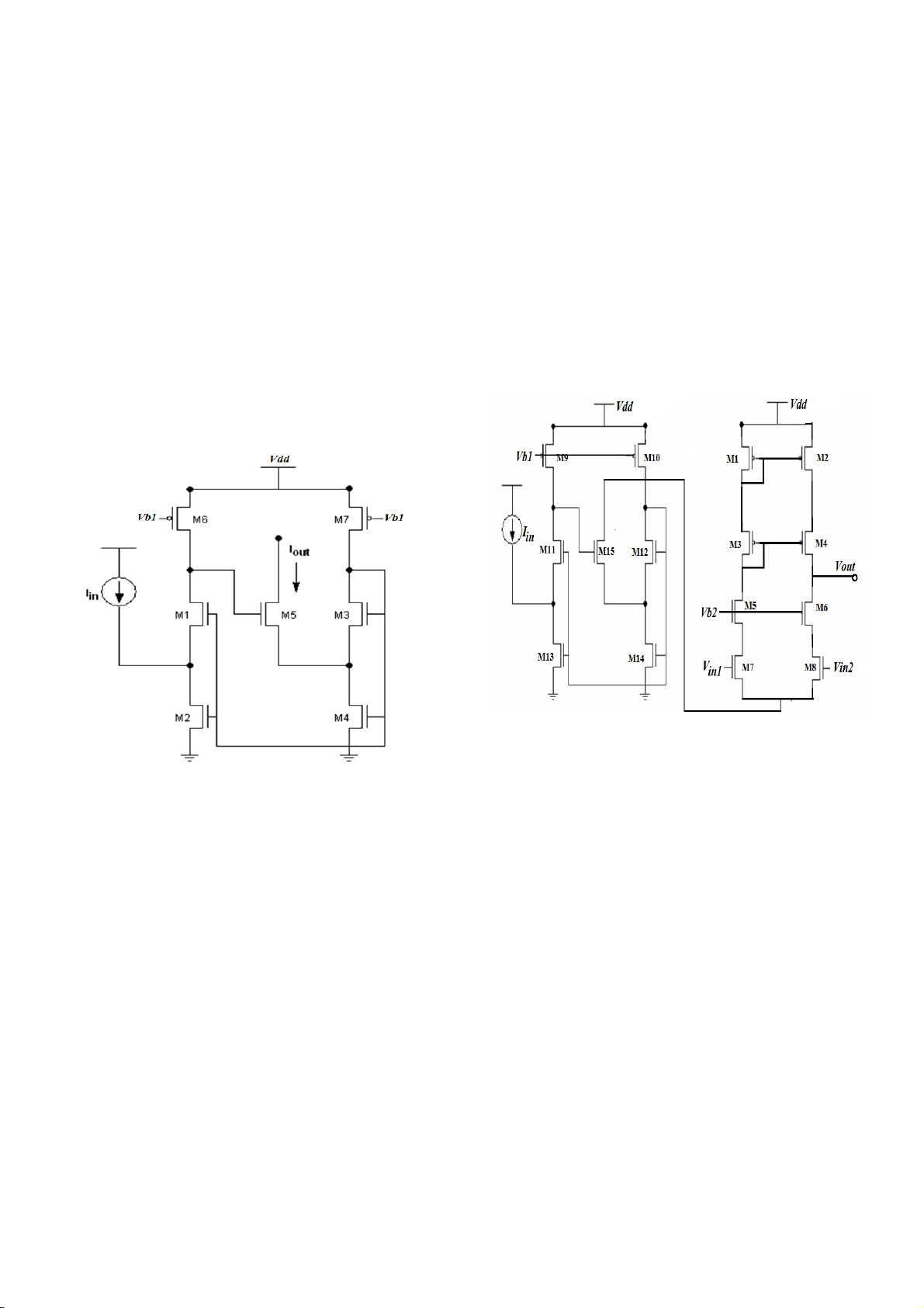
B. Proposed Current Mirror Circuit
connection of the current mirrors improves the gain of the
circuit. The tail transistor carries the tail current. It is biased
The improved high impedance low voltage current
such that it could carry the tail current of the circuit. The
mirror is modified so that the circuit can be designed for
common mode voltage of the circuit is sensitive to the
various overdrive voltages. The modification is made by
changes in the current of the tail transistor.
removing the short circuit between gate and source of the
PMOS transistors and the transistors are biased by applying a
biasing voltage at the gate of the PMOS transistors in Fig 2.
Fig.3. Telescopic Differential Amplifier using proposed current mirror circuit.
Fig.2. Proposed Current Mirror Circuit
The current through this transistor should be a constant
at a particular biasing condition. But the transistor
This helps in designing the circuit for different dependence on the temperature and other variations affect
overdrive voltages. The new current mirror circuit has a
the current through the transistor and this affect the common
biasing voltage Vb1 at the gates of transistors M6 and M7.
mode voltage of the circuit. This affects the gain of the
This voltage is selected such that the transistors obey the
circuit. So in order to maintain the gain constant the current
condition for saturation, i.e.Vgs –Vt ≥ Vds,sat, where Vgs = Vg-
of M9 should be made constant. So the tail transistor can be
Vs=Vb1-Vdd., i.e. the biasing voltage is greater than supply
replaced by a current source. [5] But it increases the power
voltage plus minimum overdrive or minimum saturation
dissipation. So a better alternative is to replace the tail
voltage. The modified circuit diagram is shown in figure.
transistor and place the output terminal of the current mirror
at the tail end of the amplifier. Current mirrors have non zero
C. Application of the current mirror circuit
mismatch and as a result the current at tail end is kept
Current mirrors [7], [8] can be used in where constant
constant. In order to increase the gain of the circuit cascade
current is needed and the following example is one such
current mirrors is used. But the output swing of telescopic op
application. The telescopic architecture [7] is the simplest
amp is relatively limited. Another drawback of telescopic
version of a single stage operational transconductance cascade is the difficulty in shorting their input and outputs,
amplifier. In it, the input differential pair injects the signal
e.g. to implement a unity gain buffer. The expected output
currents into common gate stages. Then, the circuit achieves
swing of the circuit is given by
the differential to single ended conversion with a cascode
Vb2-Vth6≤Vout≤Vb2-VGS6 +Vth8 (5) 513
In the above discussed circuit the tail transistor of the
0.17V and till the voltage reaches 0.17V, the circuit operates
differential amplifier is removed and the current mirror is in non linear region.
placed there as shown in Fig3. The desired current which is
flowing through M9 is found out. This current is given as the
input current of the current mirror. The output node of the
current mirror is connected at the tail end. So the current at
the tail end will be that at the input of the mirror. The circuit
in figure is the final circuit of the project. It is the High Gain
differential Amplifier with high output impedance current
mirror circuit at the tail end. III. SIMULATION RESULTS
The circuits are designed using 180nm TSMC
technology. In the technology the supply voltage is 1.8V and
the minimum channel length is 180nm. The power
dissipation is assumed to be 10μW. The threshold voltage of
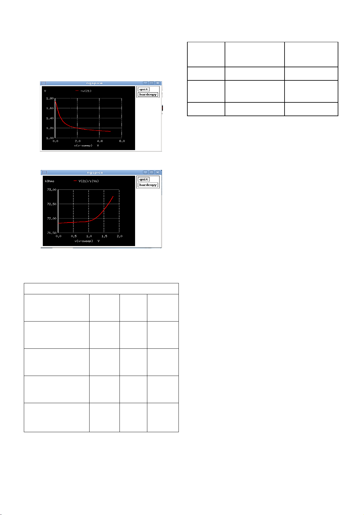
Fig.4. Output current characteristics
PMOS is -0.49V and that of NMOS is 0.5V in the 180nm
TSMC technology. The design consideration is that the
transistors are in saturation and the current equation for
transistor under saturation is given as follows, I= (μo*Cox/2) * W/L *(Vov)2 (6)
where Vov is the overdrive voltage. It is found out using
TSMC 180nm datasheet as Vov,n =0.17V and Vov,p =0.26V.
Also the power dissipation is assumed to be 10μW and using
this current through all transistors is found for Vdd of 1.8V.
Later these values are submitted to find the (W/L) ratio of all
transistors. The design values are shown in Table I. Similarly
the op-amp is also designed and design specification is
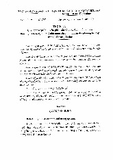
Fig.5. Output Impedance characteristics shown in Table II.
When the overdrive or drain –source voltage of M5 is
The tool used for simulation is NG SPICE. It is used
0.17V, it goes into the linear region of operation and the
because it an open source software available in the Linux
output impedance curve is linear thereafter. The maximum
FEDORA OS Electronics lab kit.
output impedance obtained is 357KΩ. This impedance is far
better than any other current mirror circuits.
A. Simulation of Current Mirror Circuit
The circuit diagram of current mirror which is shown in TABLE I.
DESIGN SPECIFICATION OF CURRENT MIRROR
Fig.2 is simulated using NG spice. The design specifications
are shown in Table I. DC analysis was done for finding the
Vdd=1.8V,Power Dissipation=10μW,
input-output characteristics of the current mirror and also to Vb1=2.1V
find the output impedance of the mirror. In order to find the Transistor Aspect Ratio(W/L)
input-output characteristics the input current was varied from
5μA o 40μA and the output current flowing through M5 was M1 204/360
found. The simulation result is shown in Fig.4. It is seen
from the graph that he output current nearly equals the input M2 568/360
current. Thus the percentage of error is less than 1%. Also
the circuit is a high output impedance current mirror circuit. M3 204/360
So it is important to find the maximum output impedance of
the circuit. The Fig.5 shows the output impedance vs. output M4 568/360
voltage of the circuit. The output voltage is increased from 0
to 1.8V and the output impedance across M5 is plotted. The M5 364/360
graph is expected to be linearly increasing with the increase
in output voltage. But it is seen in the graph that there is a
non linearity in the graph till a particular voltage, i.e. till M6 403/360
0.17V. This is because the minimum overdrive chosen is M7 403/360 514
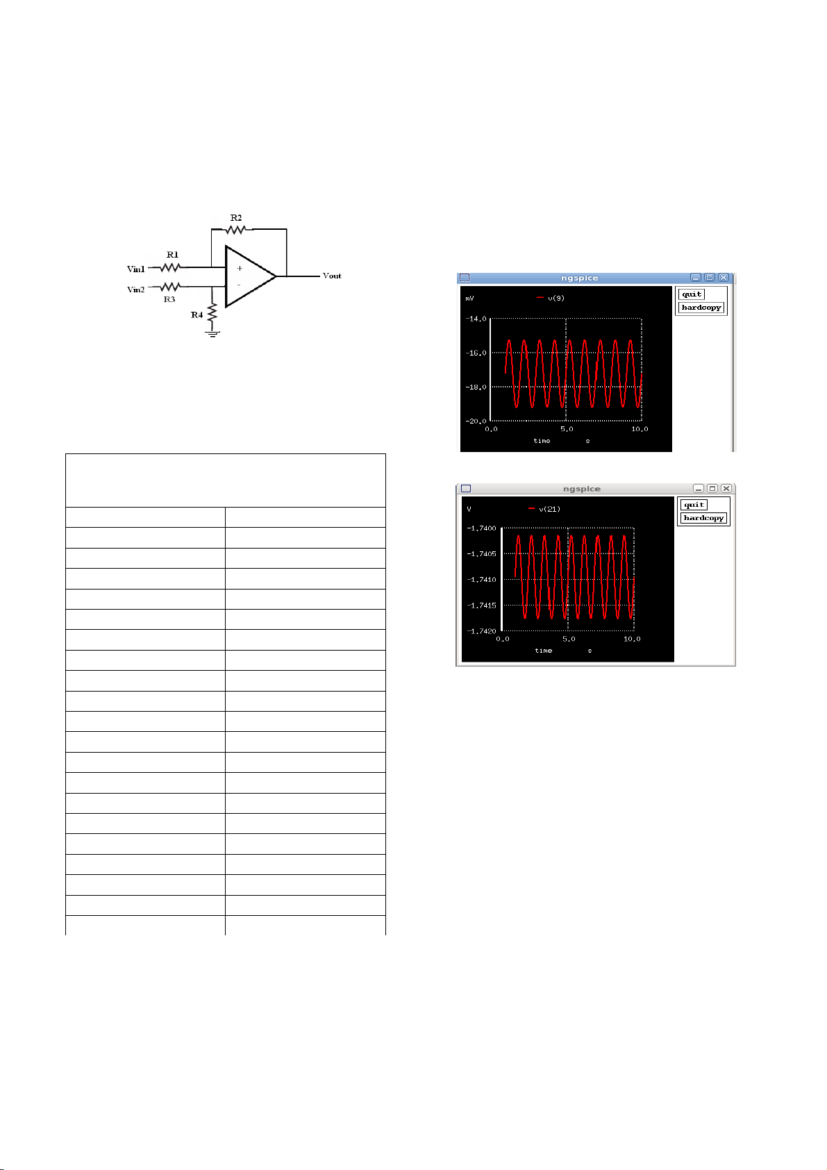
B. Simulation of Differential Amplifier Circuit
common mode and difference mode gain. The DC analysis
The telescopic differential amplifier with the proposed
was done for finding the output swing and the output
current mirror at the tail end was also simulated in NG Spice.
impedance of the circuit. In an op amp or a differential
The circuit diagram which is simulated is shown in Fig.3.
amplifier it is important to find the difference mode and
The equivalent figure is that of an op-amp. In practice the
common mode gain in order to find the CMRR of the circuit.
differential amplifier circuit differs from an op amp as they
So the transient analysis is performed to find both of these.
have some resistors connected at some nodes. This schematic
The transient analysis plotted different voltage values at is shown in Fig.6.
different time instants. Fig.7. shows the difference mode
characteristics. A difference mode gain of 82.264 was
obtained when the circuit was designed for 100. The
common mode gain obtained was 2.23 E-03. Thus the CMRR is 91.3dB.
Fig.6. Schematic of Differential Amplifier
Designing the circuit for differential amplifier [4], the
specifications are obtained which are tabulated in the Table II. TABLE II.
DESIGN SPECIFICATION OF DIFFERENTIAL AMPLIFIER (a)
Vdd=1.8V, Power Dissipation=10uW, Iin=6uA, Vb1=2.1V, Vb2=1V Transistor Aspect Ratio (W/L) M1 396/360 M2 396/360 M3 396/360 M4 396/360 M5 200/360 M6 200/360 M7 200/360 M8 200/360 (b)
Fig.7. Difference Mode characteristics (a) Input waveform (b) Output M9 403/360 waveform M10 403/360
The output swing defines the minimum and maximum M11 204/360
values of output voltages of the circuit. Theoretically the M12 204/36 outpu
0 t swing of the telescopic differential amplifier is M13 568/360
Vb-Vthn ≤ Vout ≤Vb-Vgsn +Vthn (7) M14 568/360 M15 364/360
i.e 1.3V≤Vout ≤1.63V is the expected value. Upon analysis Resistor Value t (Ω)
he output swing obtained graphically is shown in Fig.8. That R1 10K is the ou
tput swing obtained is slightly improved and is
obtained as 1.123V≤Vout ≤1.731V instead of 1.3V≤Vout R2 1000K
≤1.63V. Thus the circuit has increased output swing which R3 10K is an added adv antage of the amplifier. R4 1000K T
he output impedance of an ideal op amp is zero and in
practice it is in the range of several ohms. But when it comes
The analyses performed are transient analysis and DC
to differential amplifier the output impedance is slightly
analysis. The transient analysis was done for finding the
more and the aim is to reduce the output impedance as far as 515
possible. So it is important to plot the output impedance TABLE IV.
COMPARISON OF DIFFERENTIAL AMPLIFIERS
characteristics. The Fig.9 shows the output impedance versus
output voltage of the circuit. The maximum output Telescopic Amplifier Telescopic Amplifeir
impedance obtained is 72.8KΩ at an output voltage of 1.8V. with CM without CM
The results are shown below in Table III and IV. CMRR 91.3dB 54dB Output 72KΩ 298KΩ Impedance Output swing
1.12≤Vout ≤1.73 1.3≤Vout ≤1.63 IV. CONCLUSION
The proposed circuit offers very high impedance due to
the presence of the PMOS at both legs since no auxiliary
biasing circuit is used. It can be used for applications which
Fig.8. Output voltage characteristics
operate with very low current. One such application also is
described in the paper, i.e. the high gain improved output
swing telescopic differential amplifier. It was found that due
to the presence of the current mirror, the gain, CMRR and
the output swing of the amplifier is increased. A comparative
study is also given. The amplifier circuit can be modified to
decrease the output impedance by adding a buffer stage at the output of the amplifier. ACKNOWLEDGMENT
The author would like to thank all partners of this project for the fruitful discussions. REFERENCES
Fig.9. Output Impedance characteristics
[1] E. Raghuvaran, “A Very High Impedance Current Mirror For Bio-
medical Applications”, IEEE Transactions on Analog Circuits, 2011, TABLE III.
COMPARISON OF DIFFERENT CURRENT MIRRORS pp 828-830
[2] B. Minch, “Low-Voltage Wilson Current Mirrors in CMOS,” IEEE Vdd = 1.8V
ISCAS, New Orleans, LA, USA, 2007, pp. 2220–2223. Output
[3] Louis-Franc¸ois Tanguay, Mohamad Sawan, and Yvon Savaria, “A Iout Iout Current Mirror Impedance (Iin=40uA) (Iin=5uA)
Very-High Output Impedance Current Mirror for Very-Low Voltage (Iin=5uA)
BiomedicalAnalog Circuits,” Circuits and Systems, APCCAS 2008.
IEEE Asia Pacific Conference, 2008, pp. 642-645. Proposed Current 38.29uA 4.68uA 357KΩ
[4] Erik McCarthy, “Design and Layout of a Telescopic Operational Mirror[TSMC 180nm]
Transconductance Amplifier”, Department of Electrical and Computer
Engineering University of Maine,2009 Improved High Swing Low Voltage Wilson Current 39.2uA 4.85uA 55KΩ
[5] Jasmine, “Design And Analysis Of CMOS Telescopic Operational Mirror [1] [UMC 180nm] Amplifier”,
Thapar Institute Of Engineering Technology, 2004,unpublished. Super Wilson Current Mirror
[6] Razavi, “Design of Analog CMOS Integrated Circuits”, Tata McGraw 41.2uA 6.4uA 4.36KΩ Mirror[1] [UMC 180nm] Hill,2002, ch. 3,pp. 47-92
[7] Gray, Meyer, “Analysis and Design of Analog Integrated Circuits”,
Wiley Publishers,2001, ch.4,pp. 253-274 Low Voltage Current 37.7uA 2.64uA 47.6KΩ Mirror[1] [UMC 180nm]
[8] Allen, Holberg, “CMOS Analog Circuit Design”, Oxford University
Press,2010, ch.4, pp,134-142 516
Tài liệu liên quan:
-

Ung dung game hoa trong cac chien dich MKT
18 9 -

Bao cao Chi so TMDT Viet Nam 2025
15 8 -
Thông tư quy định về việc phân quyền, phân cấp và phân định thẩm quyền quản lý nhà nước về giáo dục cho chính quyền địa phương
24 12 -
Nghị quyết về phát huy các giá trị di sản văn hóa gắn với phát triên du lịch bền vững tỉnh Khánh Hòa đến năm 2025, định hướng đến năm 2030
14 7 -

Quyết định phê duyệt Chiến lược phát triển du lịch Việt Nam đến năm 2030
13 7