Bài kiểm tra môn Kiến trúc máy tính và Hợp ngữ nội dung bằng tiếng Anh | Đại học Sư phạm Kỹ thuật Thành phố Hồ Chí Minh
Bài kiểm tra môn Kiến trúc máy tính và Hợp ngữ nội dung bằng tiếng Anh của Đại học Sư phạm Kỹ thuật Thành phố Hồ Chí Minh với những kiến thức và thông tin bổ ích giúp sinh viên tham khảo, ôn luyện và phục vụ nhu cầu học tập của mình cụ thể là có định hướng ôn tập, nắm vững kiến thức môn học và làm bài tốt trong những bài kiểm tra, bài tiểu luận, bài tập kết thúc học phần, từ đó học tập tốt và có kết quả cao cũng như có thể vận dụng tốt những kiến thức mình đã học vào thực tiễn cuộc sống. Mời bạn đọc đón xem!
Môn: Kiến trúc máy tính và Hợp ngữ (CAAL230180) 12 tài liệu
Trường: Trường Đại học Sư phạm Kỹ thuật Thành phố Hồ Chí Minh 4.4 K tài liệu
Tác giả:


Preview text:
lOMoARcPSD| 36443508
1.What is the correct sequence of instruction cycle?
1. Fetch opcode: CPU fetches the opcode (operation code) from memory. The
address of the instruction to be fetched is determined by the program counter
(PC), which is a register holding the memory location of the next instruction.
2. Decode: CPU decodes the opcode to determine which operation needs to be
performed. This includes identifying the opcode of the instruction.
3. Calculate operand address: If the operand address needs to be calculated (e.g., in
case of indirect addressing mode), CPU performs this calculation to determine
the effective address of the operand.
4. Fetch operand: If the instruction requires an operand, CPU fetches it from
memory or from other registers within the CPU.
5. Execute: CPU performs the operation specified by the instruction, using any
operands that have been determined in the decode and calculate operand address stages.
6. Store result: The result of the operation is stored in memory or registers,
depending on the requirement. This includes storing the result of the
computation in a register or memory location, updating the program counter to
point to the next instruction, and processing any changes to the CPU state that
may be necessary (e.g., updating status flags or registers).
2. Which one best describe cache hit and cache miss?
Cache miss ratio: the number of memory accesses that CPU must retrieve from the main
memory per the total number of memory accesses
Cache hit ratio: the number of memory accesses that the CPU can retrieve from the cache
per the total number of memory accesses
3. For cache write policies, which are often used for writehit and writemiss Write-hit: Write-back Write-miss: Write-allocate
4. Choose correct features for SRAM and DRAM
DRAM: Slower access time, cheaper cost per bit, can manufacture with larger size
SRAM: Faster access time, cost more per bit, smaller size
5. Identify the correct sequence to update a page onto a flash memory?
Step 1: the entire block is being read from flash into RAM then request data in page is update
Step 2: the entire block of flash memory are erased
Step 3: The entire block from RAM then is written back to the flash memory lOMoARcPSD| 36443508
6. Choose correct set of registers for x86 processor
Data pointer to source memory in extra segment ES: SI
Pointer to variable in stack SS: BP Instruction pointer CS: IP
Data pointer in data segment DS: BX
7. Match the definition of flag bits in PSW
-contains the carry of 0 or 1 from the leftmost bit after an arithmetic operation: CF
-determine the direction for moving or comparing data between memory areas: DF
-determine whether an external interrupts are to be ignored or processed: IF
-the processor switches to singlestep mode: TF
8. What are the processor's instruction categories Data processing Control Processor I/O Processor Memory
9. In computer, how does the processor serve multiple interrupt request from devices?
The processor can not process multiple interrupt requests
Each device are assigned an interrupt priority, the device with higher priority will be served.
Device with higher priority will use interrupt enable flag
Each device are assigned an interrupt priority, the device with lower priority will be served.
10. Bus is a shared transmission medium, multiple devices connect to it but only one at a
time can successfully transmit. Which component in computer facilitates this operation? Select one: Bus Arbiter Programmed I/O
Direct Memory Access (DMA) Bus master
11. When many devices of different transmission speed connect to the same bus, the
overall system performance suffers. How did the design engineers resolved this: Select one: lOMoARcPSD| 36443508 PCI Express bus PCI bus
Split system bus into local bus and memory bus MultipleBus hierarchies
12. What are the features of directmapping cache organization? Select one or more: Thrash > low hit ratio faster Simple and inexpensive small cache memory
13. Which ones are not correct for static RAM?
Cost per bit is higher than dynamic RAM
faster than dynamic RAM because they are made from capacitor
Cheaper than dynamic RAM because simpler chip controller
Cost per bit is lower than dynamic RAM 14. Which one is not correct?
EEPROM is erasable by exposing under UV PROM is nonvolatile memory
EPROM is erasable electrically
Flash memory can only be erased electrically byte by byte
15. Which statements are correct for HDDs? Select one or more: a. Bits are stored on tracks
b. Head, Track, Sector are key parameters for access data on hard disk
c. Bits are store randomly on disk surfaces
d. Head, Track, Cylinder are key parameters for access data on hard disk
16. What is correct about the function of TRIM command in SSD? Select one:
Allow SSD to allocate memory pages in blocks properly for faster access
Allow SSD to defragment scattered data stored in separate pages
Allow OS to notify SSD the presence of occupied blocks of data which are no longer in
use and can be erased internally
Allow SSD to manage occupied pages and remove them automatically for later use
17. Which set of registers are valid for addressing a memory location? Select one or more: DS:SI lOMoARcPSD| 36443508 DS:BX SS:DI CS:IP
18. Which are valid based index addressing? Select one or more: [BX+SI] [SP+DI] [DX+SI] [BX+DI]
19. Which are valid index addressing? Select one or more: [SI] [DX] [BX] [BP]
20. 8088 is 16 bit processor, the maximum addressable memory is: Select one: 64M 1024K 640K 640M
21. Which are correct about the data registers of IA32 processors: Select one or more:
-Lower halves of the 16registers an be used as 8bit data registers: AH,AL,BH,BL,CH,CL,DH,DL
-complete 32bit registers: EAX, EBX, ECX, EDX
-Lower halves of the 32registers an be used as 4 16bit data registers: AX,BX,CX,DX -
Higher halves of the 32bit registers can be used as 16bit registers:
EAH,EAL,EBH,EBL,ECH,ECL,EDH,EDL
22. Which are correct about 32 bit index registers of IA32 processors: Select one or more:
EDI: 32 bit pointer to destination memory in data movement instructions
ESH,EDH: 16 bit pointers to higher memory above 1M
DI: 16 bit pointer to destination memory in data movement instructions lOMoARcPSD| 36443508
SI: 16 bit pointer to source memory in data movement instructions ESI:
32 bit pointer to source memory in data movement instructions
23. Which statement is correct about interrupt vector table? Select one or more:
Store in the ending area of 1024K of the main memory
Take up 1024 bytes in the main memory Store on disk
Store in the beginning area of the main memory
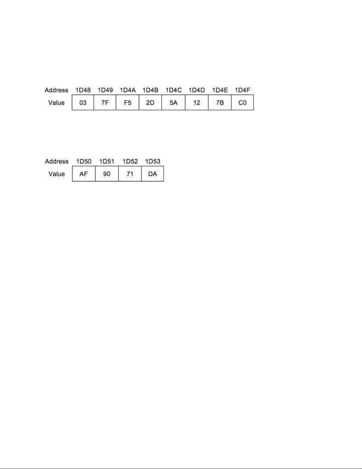
24. Part of memory as shown in figure
The value of DX register follows the execution of MOV DX, [1D4D] is 127B. What is
the endian type of this computer system Select one: littleendian levelendian bigendian nonendian
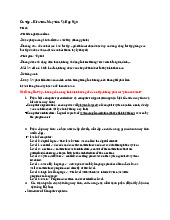
25. Part of memory as shown in figure
The value of BX register follows the execution of MOV BX, [1D49] is F57F. What is the
endian type of this computer system Select one: levelendian bigendian littleendian nonendian
26. What best describe the Spatial and Temporal Locality?
Temporal locality: be exploited by keeping recently used instruction and data in cache
memory and by exploiting a cache hierarchy
Spatial locality: be exploited by using larger cache blocks and by incorporating
prefetching mechanisms into the cache control logic
27. To evaluate processor performance, the following indicators and formulas are used:
Which of the following system attributes affects cycle time Select one or more: Processor implementation Compiler technology Instruction set architecture Cache and memory hierarchy lOMoARcPSD| 36443508
28. Key parameters to consider when evaluating processor hardware include: Select one or more: reliability performance power consumption databus size size Address bus size cost
29. A memory chip has 12 address pins, determine the maximum memory words of this chip? Select one: 2048K 2048 4000 4096
30. Which of the following best describe the memory chip with pinout as shown below: DQ: Data pinout Select one: DRAM 64Kx4bit SRAM 256Kx1bit DRAM 16Kx4bit SDRAM 64Kx4bit
31. Choose the correct structure of memory chip as shown below lOMoARcPSD| 36443508 Note: DQ: Data pinout Select one: DRAM 2Kx8bit SRAM 1Kx16bit SRAM 2Kx8bit DRAM 1Kx16bit
32. The three key characteristics of memory are: capacity, access time and cost. Which of
the following relationships hold for a variety of memory technologies? Select one or more:
Faster access time, greater cost per bit
Higher capacity, higher access time
Greater capacity, smaller cost per bit
Greater capacity, slower access time
33. A SRAM memory chip labeled 32x8bit. Which of the following is correct pinout
regarding address and data lines? Select one: 32 address pins, 3 data pins
32 address pins, 4 data pins 5 address pins, 3 data pins 15 address pins, 8 data pins
34. In the interconnection system, the number of address lines are governs by Select one: lOMoARcPSD| 36443508 I/O Module CPU data bus line Memory size 35. Select one or more: Increasing access time Decreasing cost per bit
Decreasing frequency of access by the
processor the processor accesses more often Increasing capacity
36. Identified correct addressing mode of the following instructions? MOV AX, BX Register MOV BP, [BX+SI] Base plus index MOV AX, ARRAY [BX+SI] Base relative plus index MOV AX, [BX] Register indirect MOV AX,[1234h] Direct MOV AX, 3540h Immediate
37. Part of computer memory is shown in figure
What is the value of AX register after instruction MOV AX, [1D4B] executed Answer: 5A2D
38. Part of memory shown in figure
What is the value of EAX follow the execution of this code MOV BX, 1D4C lOMoARcPSD| 36443508 MOV EAX, [BX] Answer: 125A
39. the memory stack area of a program shown in figure
The value of SP register is 1D48. What is the value of SI follows the executionof POP SI Answer: 1D48
40. the memory stack area of a program shown in figure
The value of SP register is 1D50. What is the value of SP follows the execution of PUSH SI Answer: 1D4F
41. Choose correct RAID volume definitions for a request 2T storage.
RAID 1 Mirror volume 2 x 2T HDDs are needed, no data lost when the primary storage fails
Spanned Volume 2T HDD + more HDDs to extend storage, no fault tolerance, data lost when one HDD fails
RAID 0 Striped volume 2 x 1T HDDs are needed, enhance data transfer, no fault tolerance, data lost when one HDD fails RAID5 Volume
At least 3 x 2T HDDs, faulttolerance, no data lost, no downtime
42. Consider a 32bit microprocessor whose bus cycle is the same duration as that of a
16bit microprocessor. Assume that, on average, 30% of the operands and instructions
are 32 bits long, 40% are 16 bits long, and 30% are only 8 bits long. Calculate the
improvement achieved when fetching instructions and operands with the 32bit microprocessor? Select one: 10% 15% 17% 23%
43. Consider a magnetic disk drive with 8 surfaces, 512 tracks per surface, and 64 sectors
per track. Sector size is 1 kB, the average seek time is 10.2 ms and the drive rotates at
3600 rpm. What is average access time. Given: Rotational delay = 1/(2r), where r is
the rotational speed in revolutions per second lOMoARcPSD| 36443508 Answer: 16.3 ms
Tài liệu liên quan:
-

Bài giảng Introduction môn Kiến trúc máy tính | Trường Đại học Sư phạm Kỹ thuật Thành phố Hồ Chí Minh
65 33 -

Bài giảng Computer evolution & designing for performance môn Kiến trúc máy tính | Trường Đại học Sư phạm Kỹ thuật Thành phố Hồ Chí Minh
54 27 -
Ôn cuối kỳ Môn Kiến trúc máy tính và Hợp ngữ | Đại học Sư phạm Kỹ thuật Thành phố Hồ Chí Minh
270 135 -
Trắc nghiệm về kiến trúc máy tính và lập trình Assembly | Môn Kiến trúc máy tính và Hợp ngữ - Đại học Sư phạm Kỹ thuật Thành phố Hồ Chí Minh
223 112 -
Chapter 01 Môn Kiến trúc máy tính và Hợp ngữ | Đại học Sư phạm Kỹ thuật Thành phố Hồ Chí Minh
171 86