Báo cáo cuối kỳ môn Hardware/Software Codesign đề tài "Creating a process or system" bằng tiếng Anh
Báo cáo cuối kỳ môn Hardware/Software Codesign đề tài "Creating a process or system" bằng tiếng Anh của Đại học Sư phạm Kỹ thuật Thành phố Hồ Chí Minh với những kiến thức và thông tin bổ ích giúp sinh viên tham khảo, ôn luyện và phục vụ nhu cầu học tập của mình cụ thể là có định hướng ôn tập, nắm vững kiến thức môn học và làm bài tốt trong những bài kiểm tra, bài tiểu luận, bài tập kết thúc học phần, từ đó học tập tốt và có kết quả cao cũng như có thể vận dụng tốt những kiến thức mình đã học vào thực tiễn cuộc sống. Mời bạn đọc đón xem!
Môn: Hardware/Software Codesign (HSCD446164) 10 tài liệu
Trường: Trường Đại học Sư phạm Kỹ thuật Thành phố Hồ Chí Minh 4.4 K tài liệu
Tác giả:


Preview text:
lOMoARcPSD| 36625228
HCMC UNIVERSITY OF TECHNOLOGY AND EDUCATION
FACULTY OF HIGH QUALITY TRAINING FINALPROJECT
Course name: HARDWARE/SOFTWARE CODESIGN
CREATINGAPROCESSORSYSTEM : lOMoARcPSD| 36625228 ACKNOWLEDGEMENT
To complete the Hardware/Software Codesign subject, we would like to express our
heartfelt gratitude to Assoc. Prof. Phan Van Ca has enthusiastically guided and equipped
us with the necessary helpful knowledge this semester. Furthermore, he has directly
guided and created all conditions to help us during the process of Hardware/Software Codesign.
Due to the project's short implementation time, the topic's limited knowledge,
limitations, and errors have not been completely overcome. We look forward to
receiving your advice and suggestions. Student lOMoARcPSD| 36625228 CONTENT
ACKNOWLEDGEMENT .............................................................................................. i
CONTENT ..................................................................................................................... ii
FIGURE LIST ............................................................................................................... iv
PART 1. INTRODUCTION .......................................................................................... 1
1.1. Introduction ......................................................................................................... 1
1.2. Purpose and requirements .................................................................................... 1
1.3. Layout .................................................................................................................. 1
PART 2. CREATING A PROCESSOR SYSTEM ........................................................ 1
2.1. Embedded System Design in Zynq using IP Integrator ...................................... 1
2.1.1. Embedded Design Architecture in Zynq .................................................. 1
2.1.2. The PS and the PL .................................................................................... 2
2.1.3. Vivado ...................................................................................................... 2
2.2. Creating IP-XACT Hardware Accelerator .......................................................... 3
2.2.1. Port-Level Interfaces ................................................................................ 3
2.2.2. Interface Modes ........................................................................................ 4
2.2.3. Native AXI Slave Lite Interface .............................................................. 4
2.2.4. Controllable Register Maps in AXI4 Lite ................................................ 4
2.2.5. Native AXI4 Master ................................................................................. 4
2.2.6. Burst Accesses Inferred for AXI4 Master ................................................ 5
2.2.7. Byte-Enable Accesses on AXI4 Master ................................................... 5
2.2.8. AXI4 Port Bundling ................................................................................. 5
2.2.9. AXI4 Stream Interface: Ease of Use ........................................................ 6
2.2.10. Generate the hardware accelerator ......................................................... 6
2.2.11. Generated impl Directory ....................................................................... 6
2.3. Integrating the Hardware Accelerator in AXI System ........................................ 6
PART 3. CREATING A PROCESSOR SYSTEM LAB ............................................... 7
3.1. Create a New Project ........................................................................................... 7
3.2. Run C Simulation ................................................................................................ 9
3.3. Synthesize the Design ........................................................................................ 10
3.4. Run RTL/C CoSimulation ................................................................................. 11 lOMoARcPSD| 36625228
3.5. Setup IP-XACT Adapter ................................................................................... 12
3.6. Generate IP-XACT Adapter .............................................................................. 13
3.7. Create a Vivado Project ..................................................................................... 15
3.8. Export to SDK and create Application Project ................................................. 19
3.9. Verify the Design in Hardware .......................................................................... 20
REFERENCE ............................................................................................................... 23 lOMoARcPSD| 36625228 FIGURE LIST
Figure 1: The design under consideration ........................................................................9
Figure 2: The header file................................................................................................ 10
Figure 3: Initial part of the generated output in the Console view ................................11 Figure 4: Generated interface signals
.............................................................................12
Figure 5: Selecting the AXI4LiteS adapter and naming bundle ....................................13
Figure 6: Applying bundle to assign y output to AXI4Lite adapter ..............................14
Figure 7: Export RTL Dialog ......................................................................................... 15
Figure 8: IP-XACT adapter generated ........................................................................... 15 Figure 9: Adapter’s drivers directory
.............................................................................16
Figure 10: Block design made for Pynq .........................................................................17
Figure 11: Setting path to IP Repositories ..................................................................... 18
Figure 12: Generated design after IRQ_F2P interface enabled .....................................19 Figure 13: Generated address map
.................................................................................20 lOMoARcPSD| 36625228 PART 1. INTRODUCTION 1.1. Introduction
This project will present you with the process of using Vivado and IP Integrator to
create a complete Zynq ARM Cortex-A9 based processor system targeting the ZyBoard
Zynq development board. You will use the Block Design feature of IP Integrator to
configure the Zynq PS and add IP to create the hardware system, and SDK to create an
application to verify the design functionality. It will also guide you through the process
of profiling an application and analyzing the output.
1.2. Purpose and requirements a) Purpose
This lab introduces a design flow to generate a IP-XACT adapter from a design
using Vivado HLS and using the generated IP-XACT adapter in a processor system
using IP Integrator in Vivado. b) Requirements
After completing this lab, you will be able to: -
Understand the steps and directives involved in creating an IP-XACT
adapter from a synthesized design in Vivado HLS -
Create a processor system using IP Integrator in Vivado -
Integrate the generated IP-XACT adapter into the created processor system. 1.3. Layout
The report is divided into 4 parts: Part 1. Introduction
Part 2. Creating a Processor System
Part 3. Creating a Processor System Lab Part 4. Conclusion
PART 2. CREATING A PROCESSOR SYSTEM
2.1. Embedded System Design in Zynq using IP Integrator
2.1.1. Embedded Design Architecture in Zynq
Embedded design in Zynq is based on: – Processor and peripherals
• Dual ARM® Cortex™ -A9 processors of Zynq-7000 AP SoC • AXI interconnect lOMoARcPSD| 36625228 • AXI component peripherals
• Reset, clocking, debug ports
– Software platform for processing system • Standalone OS • C language support • Processor services • C drivers for hardware – User application
• Interrupt service routines (optional)
2.1.2. The PS and the PL
The Zynq-7000 AP SoC architecture consists of two major sections: – PS: Processing system
• Dual ARM Cortex-A9 processor based (Single core versions available)
• Multiple peripherals• Hard silicon core – PL: Programmable logic
• Uses the same 7 series programmable logic
– Artix™-based devices: Z-7010, Z-7015, and Z-7020 (high-range I/O banks only)
– Single core versions: Z-7017S, Z-7012S, and Z-7014S
– Kintex™-based devices: Z-7030, Z-7035, Z-7045, and Z-7100 (mix of high-rangeand high-performance I/O banks) 2.1.3. Vivado
What are Vivado, IP Integrator and SDK?
– Vivado is the tool suite for Xilinx FPGA design and includes capability for embedded system design
• IP Integrator, is part of Vivado and allows block level design of the hardware part ofan Embedded system • Integrated into Vivado
• Vivado includes all the tools, IP, and documentation that are required for
designingsystems with the Zynq-7000
AP SoC hard core and/or Xilinx MicroBlaze soft core processor
• Vivado + IPI replaces ISE/EDK lOMoARcPSD| 36625228
– SDK is an Eclipse-based software design environment
• Enables the integration of hardware and software components • Links from Vivado
Vivado is the overall project manager and is used for developing non-embedded
hardware and instantiating embedded systems
– Vivado/IP Integrator flow is recommended for developing Zynq embedded systems.
Embedded System Design using Vivado
2.2. Creating IP-XACT Hardware Accelerator
2.2.1. Port-Level Interfaces
The AXI4 interfaces supported by Vivado HLS include – The AXI4-Stream (axis) •
Specify on input arguments or output arguments only, not on input/output
arguments– The AXI4 master (m_axi) •
Specify on arrays and pointers (and references in C++) only. You can group
multiple arguments into the same AXI4-Lite interface using the bundle option – The AXI4-Lite (s_axilite)
• Specify on any type of argument except arrays. You can group multiple arguments into
the same AXI4-Lite interface using the bundle option. lOMoARcPSD| 36625228 2.2.2. Interface Modes Native AXI Interfaces
– AXI4 Slave Lite, AXI4 Master, AXI Stream supported by INTERFACE directive
• Provided in RTL after Synthesis
• Supported by C/RTL Co-simulation
• Supported for Verilog and VHDL BRAM Memory Interface
– Identical IO protocol to ap_memory
– Bundled differently in IP Integrator
• Provides easier integration to memories with BRAM interface
2.2.3. Native AXI Slave Lite Interface
Interface Mode: s_axilite
– Supported with INTERFACE directive
– Multiple ports may be grouped into the same Slave Lite interface
• All ports which use the same bundle name are grouped Grouped Ports
– Default mode is ap_none for input ports
– Default mode is ap_vld for output ports
– Default mode ap_ctrl_hs for function (return port)
– Default mode can be changed with additional INTERFACE Directives.
2.2.4. Controllable Register Maps in AXI4 Lite
Assigning offset to array (RAM) interfaces
– Specified value is offset to base of array
– Array’s address space is always contiguous and linear
C Driver Files include offset information
– In generated driver file xhls_sig_gen_bram2axis.h
2.2.5. Native AXI4 Master Interface Mode: m_axi
– Supported with INTERFACE directive Options
– Multiple ports may be grouped into the same AXI4 Master interface
• All ports which use the same bundle name are grouped lOMoARcPSD| 36625228
– Depth option is required for C/RTL co-simulation
• Required for pointers, not arrays
• Set to the number of values read/written
– Option to support offset or base address
2.2.6. Burst Accesses Inferred for AXI4 Master
There are two types of accesses on an AXI Master: Single Access and Burst Access
– Burst accesses are more efficient
– Burst access has until now required the use of memcpy()
Burst Accesses are now inferred
– From operations in a for-loop and from sequential operations in the code
– However: there are some limitations
• Single for-loops only, no nested loops
2.2.7. Byte-Enable Accesses on AXI4 Master
Byte-Enable Accesses Support on AXI4 Master Interfaces
– Single bytes are now written and read
– Improved AXI4 Master performance Improved Performance – This code uses 8-bit data
• Previously, accessing this required reading/writing full 32-bit
• This implied a required read-modify-write behavior: Impacted performance
– Similar performance improvement when accessing struct members
• Also often implied read-modify-write behavior – Improved Port Bundling
• Variables of different sizes can be grouped into same AXI4 Master port.
2.2.8. AXI4 Port Bundling
AXI4 Master and Lite Port Bundling
– The bundle options groups arguments into the same AXI4 port– For
example, group 3 arguments into AXI4 port “ctrl” :
Arguments can be Bundled into AXI4 Master and AXI4 Lite ports
– If no bundle name is used a default name is used for all arguments
• All go into a single AXI4 Master or AXI4 Lite
• Default name applied if no –bundle option is used lOMoARcPSD| 36625228
– Group different sized variables into an AXI4 Master port
2.2.9. AXI4 Stream Interface: Ease of Use
Native Support for AXI4 Stream Interfaces
– Native = An AXI4 Stream can be specified with set_directive_interface
• No longer required to set the interface then add a resource
• This AXI4 Stream interface is part of the HDL after synthesis
• This AXI4 Stream interface is simulated by RTL co-simulation
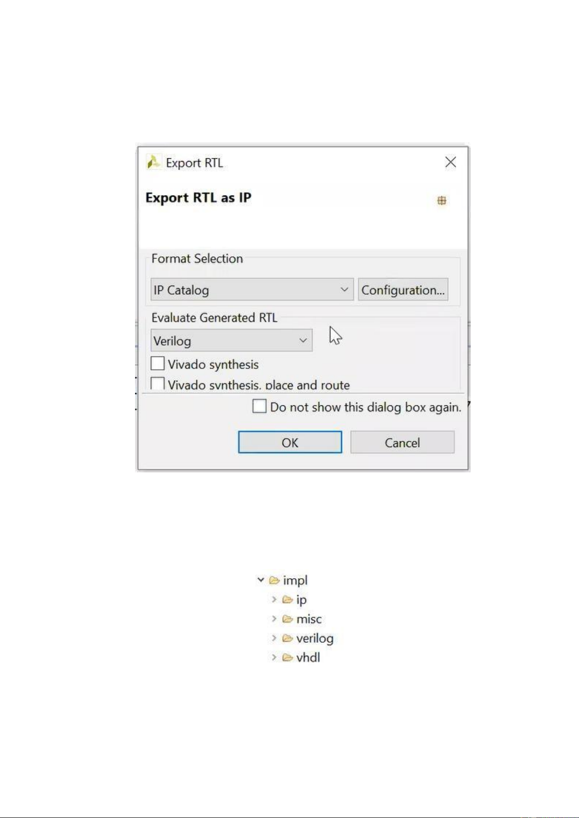
2.2.10. Generate the hardware accelerator
Select Solution > Export RTL
Select IP Catalog, System Generator for Vivado or design check point (dcp) Click
on Configuration… if you want to change the version number or other information – Default is v1_00_a Click on OK –
The directory (ip) will be generated under the impl folder under the current
projectdirectory and current solution –
RTL code will be generated, both for Verilog and VHDL languages in their respective folders
2.2.11. Generated impl Directory
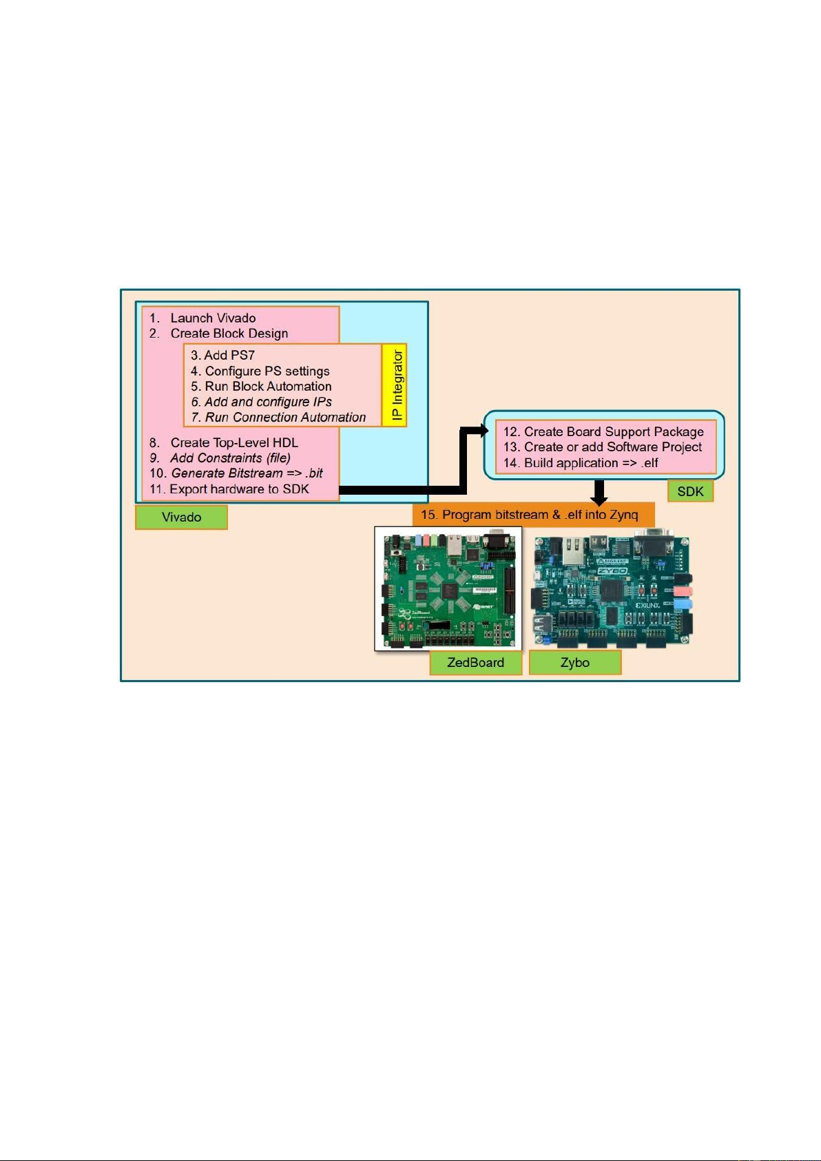
2.3. Integrating the Hardware Accelerator in AXI System
Create a new Vivado project, or open an existing project Invoke IP Integrator
Construct(modify) the hardware portion of the embedded design by adding the IP-XACT lOMoARcPSD| 36625228
Create (Update) top level HDL wrapper
Synthesize any non-embedded components and implement in Vivado
Export the hardware description, and launch XSDK
Create a new software board support package and application projects in the XSDK
Compile the software with the GNU cross-compiler in XSDK
Download the programmable logic’s completed bitstream using Xilinx Tools > Program FPGA in XSDK
Use XSDK to download and execute the program (the ELF file).
PART 3. CREATING A PROCESSOR SYSTEM LAB
3.1. Create a New Project
Create a new project in Vivado HLS targeting xc7z020clg400-1 device
1. Select Start > Xilinx Design Tools > Vivado HLS 2017.4 A Getting
Started GUI will appear.
2. In the Getting Started section, click on Create New Project. The New Vivado HLS Project wizard opens.
3. Click Browse… button of the Location field, browse to {labs}\lab4, and then click OK.
4. For Project Name, type fir.prj and click Next.
5. In the Add/Remove Files for the source files, type fir as the function name (the
provided source file contains the function, to be synthesized, called fir).
6. Click the Add Files… button, select fir.c and fir_coef.dat files from the
{sources}\lab4 folder, and then click Open. 7. Click Next.
8. In the Add/Remove Files for the testbench, click the Add Files… button, select
fir_test.c file from the {sources}\lab4 folder and click Open. 9. Click Next.
10. In the Solution Configuration page, leave Solution Name field as solution1 and
make sure the clock period as 8. Leave Uncertainty field blank.
11. Click on the Part’s Browse button and using the Parts Specify option, select xc7z020clg400-1. lOMoARcPSD| 36625228 12. Click Finish.
You will see the created project in the Explorer view. Expand various sub-folders to
see the entries under each sub-folder.
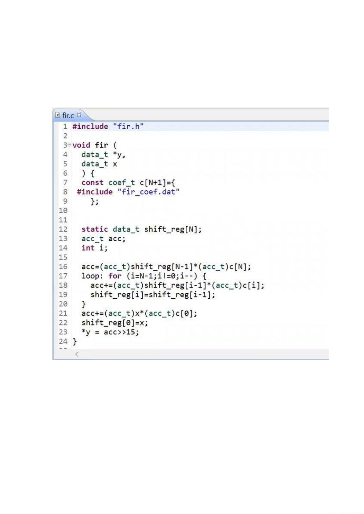
13. Double-click on the fir.c under the source folder to open its content in the information pane.
Figure 1: The design under consideration
The FIR filter expects x as a sample input and pointer to the computed sample out
y. Both of them are defined of data type data_t. The coefficients are loaded in array c of
type coef_t from the file called fir_coef.dat located in the current directory. The
sequential algorithm is applied and accumulated value (sample out) is computed in variable acc of type acc_t.
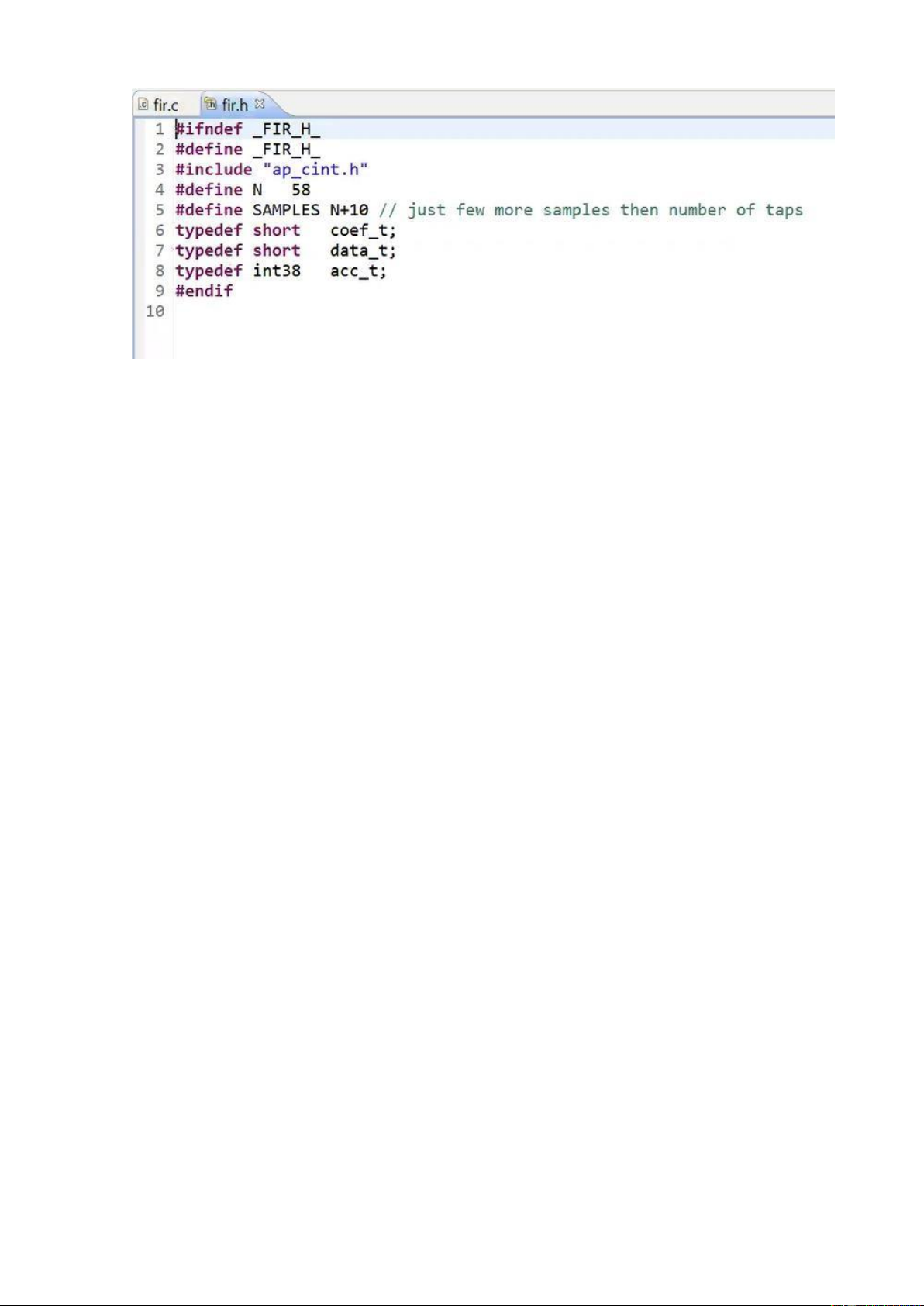
14. Double-click on the fir.h in the outline tab to open its content in the information pane. lOMoARcPSD| 36625228
Figure 2: The header file
The header file includes ap_cint.h so user defined data width (of arbitrary precision)
can be used. It also defines number of taps (N), number of samples to be generated (in
the testbench), and data types coef_t, data_t, and acc_t. The coef_t and data_t are short
(16 bits). Since the algorithm iterates (multiply and accumulate) over 59 taps, there is a
possibility of bit growth of 6 bits and hence acc_t is defined as int38. Since the acc_t is
bigger than sample and coefficient width, they have to cast before being used (like in
lines 16, 18, and 21 of fir.c).
15. Double-click on the fir_test.c under the testbench folder to open its content in the information pane.
Notice that the testbench opens fir_impulse.dat in write mode, and sends an impulse (first sample being 0x8000. 3.2. Run C Simulation
Run C simulation to observe the expected output.
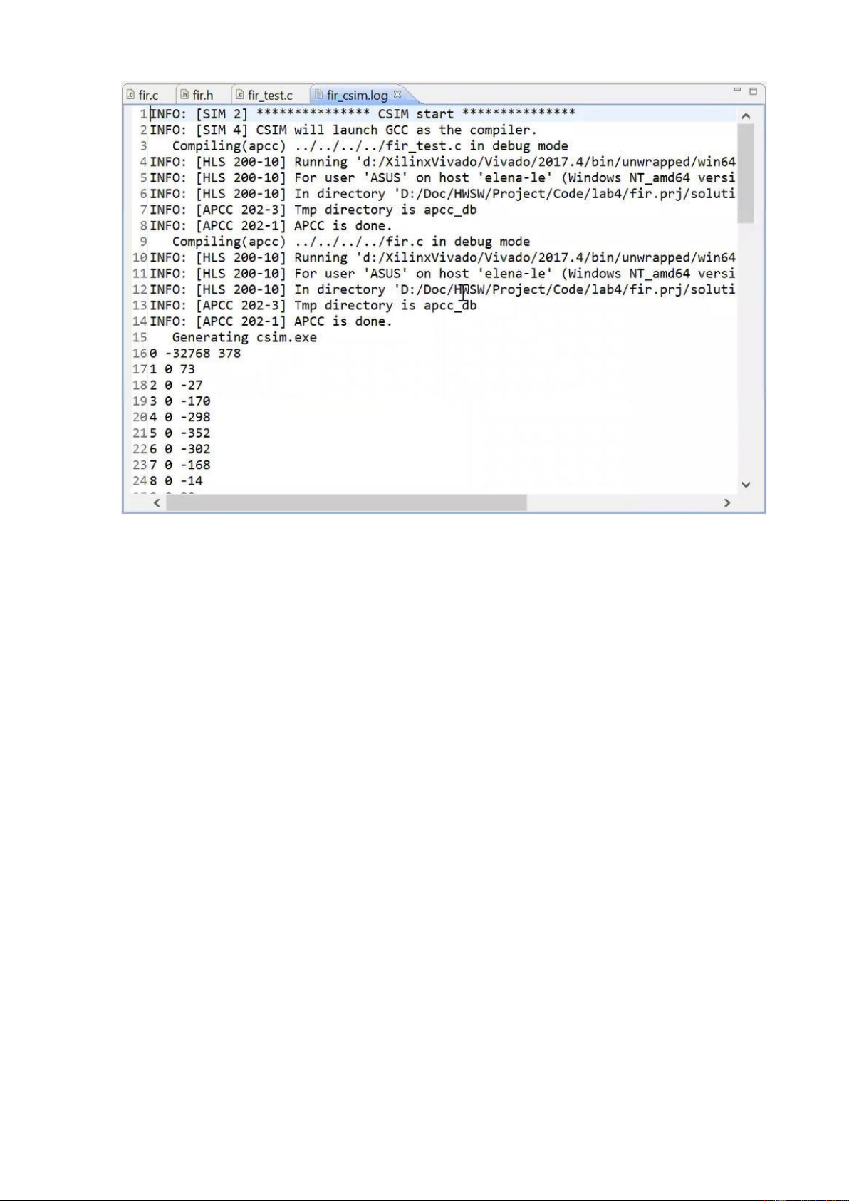
1. Select Project > Run C Simulation or click on the button from the tools bar buttons,
and click OK in the C Simulation Dialog window.
The testbench will be compiled using apcc compiler and csim.exe file will be generated.
The csim.exe will then be executed and the output will be displayed in the console view. lOMoARcPSD| 36625228
Figure 3: Initial part of the generated output in the Console view
3.3. Synthesize the Design
Synthesize the design with the defaults. View the synthesis results and answer
the question listed in the detailed section of this step.
1. Select Solution > Run C Synthesis > Active Solution to start the synthesis process.
2. When synthesis is completed, several report files will become accessible and
theSynthesis Results will be displayed in the information pane.
3. The Synthesis Report shows the performance and resource estimates as well as
estimated latency in the design.
4. Using scroll bar on the right, scroll down into the report and answer the followingquestion. Estimated clock period: 8ns Worst case latency: 175 Number of DSP48E used: 0
Number of BRAMs used: 3 Number of FFs used: 168 Number of LUTs used: 157
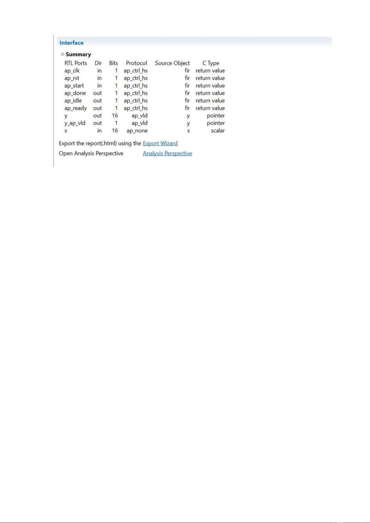
5. The report also shows the top-level interface signals generated by the tools. lOMoARcPSD| 36625228
Figure 4: Generated interface signals
You can see the design expects x input as 16-bit scalar and outputs y via pointer of
the 16-bit data. It also has ap_vld signal to indicate when the result is valid.
Add PIPELINE directive to the loop and re-synthesize the design. View the synthesis results.
1. Make sure that the fir.c is open in the information view.
2. Select the Directive tab, and apply the PIPELINE directive to the loop.
3. Select Solution > Run C Synthesis > Active Solution to start the synthesis process.
4. When synthesis is completed, the Synthesis Results will be displayed in the information pane.
5. Note that the latency has reduced to 63 clock cycles. The DSP48 and
BRAMconsumption remains same; however, LUT and FF consumptions have slightly increased.
3.4. Run RTL/C CoSimulation
Run the RTL/C Co-simulation, selecting Verilog. Verify that the simulation passes.
1. Select Solution > Run C/RTL Co-simulation or click on the button to open the
dialog box so the desired simulations can be run.
2. Select the Verilog option and click OK.
The Co-simulation will run, generating and compiling several files, and then
simulating the design. In the console window you can see the progress. When done the
RTL Simulation Report shows that it was successful and the latency reported was 62. lOMoARcPSD| 36625228
3.5. Setup IP-XACT Adapter
Add INTERFACE directive to create AXI4LiteS adapters so IP-XACT
adapter can be generated during the RTL Export step.
1. Make sure that fir.c file is open and in focus in the information view.
2. Select the Directive tab.
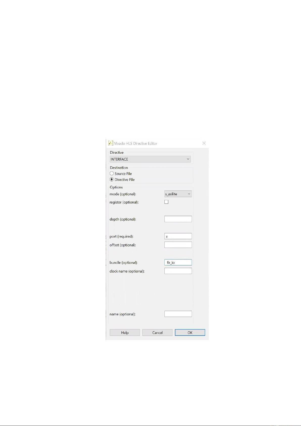
3. Right-click x, and click on Insert Directive….
4. In the Vivado HLS Directive Editor dialog box, select INTERFACE using the drop- down button.
5. Click on the button beside mode (optional). Select s_axilite.
6. In the bundle (optional) field, enter fir_io and click OK.
Figure 5: Selecting the AXI4LiteS adapter and naming bundle
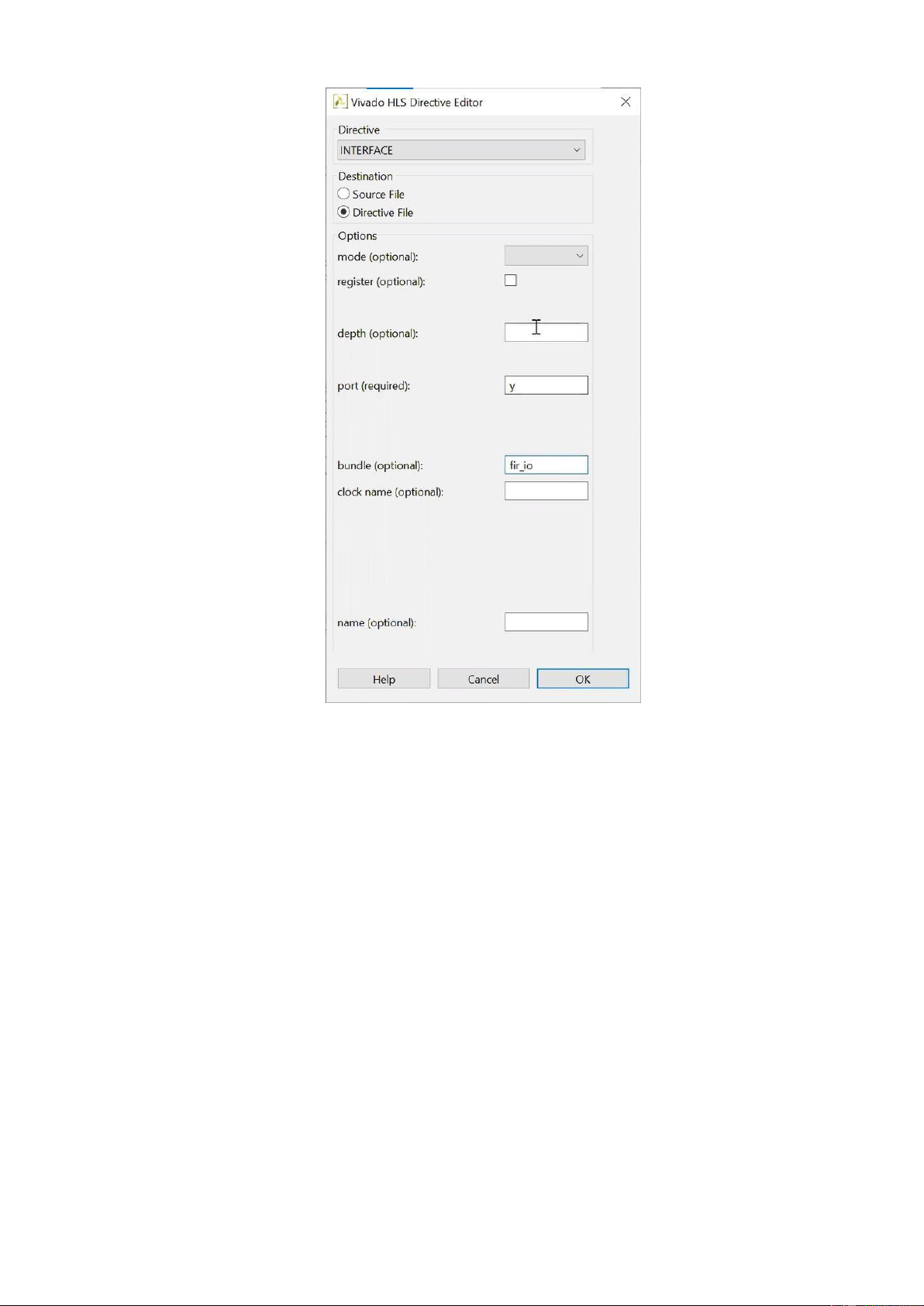
7. Similarly, apply the INTERFACE directive (including bundle) to the y output. lOMoARcPSD| 36625228
Figure 6: Applying bundle to assign y output to AXI4Lite adapter
8. Apply the INTERFACE directive to the top-level module fir to include ap_start,
ap_done, and ap_idle signals as part of bus adapter (the variable name shown will be
return). Include the bundle information too.
Note that the above steps will create address maps for x, y, ap_start ap_valid,
ap_done, and ap_idle, which can be accessed via software. Alternately, ap_start,
ap_valid, ap_done, ap_idle signals can be generated as separate ports on the core by not
applying RESOURCE directive to the top-level module fir. These ports will then have
to be connected in a processor system using available GPIO IP.
3.6. Generate IP-XACT Adapter
Re-synthesize the design as directives have been added. Run the RTL Export
to generate the IP-XACT adapter.
1. Since the directives have been added, it is safe to re-synthesize the design.
SelectSolution > Run C Synthesis > Active Solution lOMoARcPSD| 36625228
Check the Interface summary at the bottom of the Synthesis report to see the
interface that has been created.
2. Once the design is synthesized, select Solution > Export RTL to open the dialog
box so the desired IP can be generated. An Export RTL Dialog box will open.
Figure 7: Export RTL Dialog
3. Click OK to generate the IP-XACT adapter.
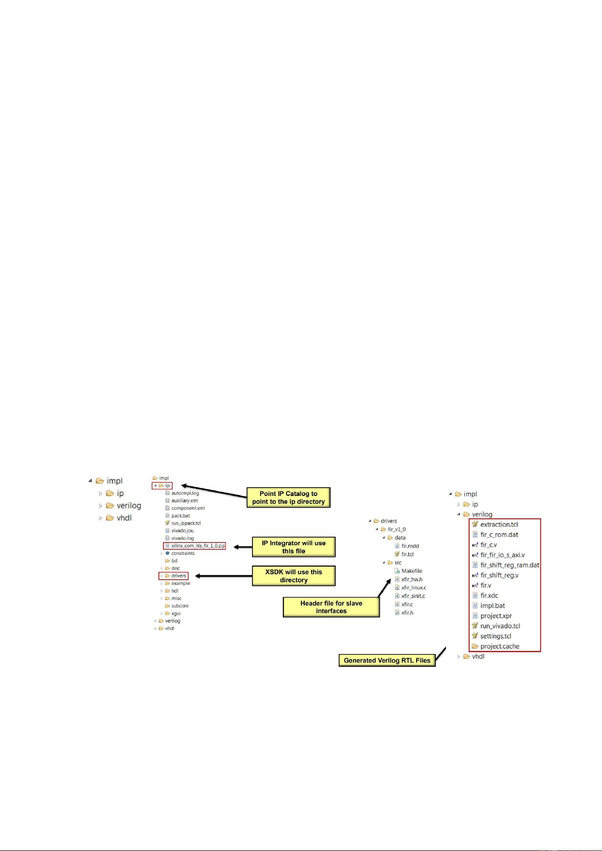
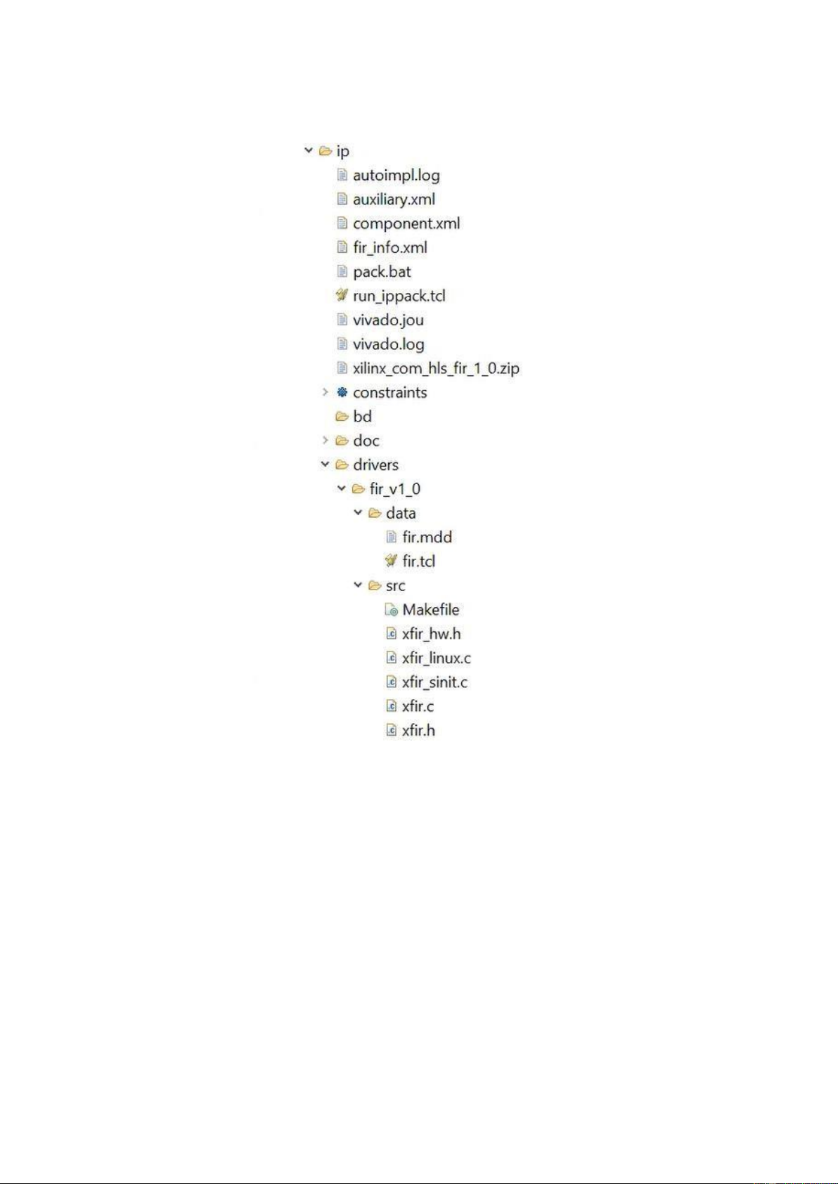
4. When the run is completed, expand the impl folder in the Explorer view and observe
various generated directories, such as ip, misc, verilog and vhdl.
Figure 8: IP-XACT adapter generated
Expand the ip directory and observe several files and sub-directories. One of the
sub-directory of interest is the drivers directory which consists of header, c, tcl, mdd, lOMoARcPSD| 36625228
and makefile files. Another file of interest is the zip file, which is the ip repository file
that can be imported in an IP Integrator design
Figure 9: Adapter’s drivers directory
5. Close Vivado HLS by selecting File > Exit.
3.7. Create a Vivado Project
Create an empty project targeting the part xc7z020clg400-1, and run the
provided tcl script to create an initial system.
1. Open Vivado by selecting Start > Xilinx Design Tools > Vivado 2018.2 2. Click
Create New Project to start the wizard. You will see the Create a New Vivado Project
dialog box. Click Next.
3. Click the Browse button of the Project Location field of the New Project form,
browse to {labs}\lab4, and click Select. lOMoARcPSD| 36625228
4. Enter audio in the Project Name field. Make sure that the Create Project
Subdirectory box is checked. Click Next.
5. Select RTL Project in the Project Type form, and click Next.
6. Click Next to skip Add Sources dialog boxes.
7. Click Next to skip Add Constraints dialog boxes
8. In the Default Part form, select Parts, and select xc7z020clg400-1. Click Next.
9. Check the Project Summary and click Finish to create an empty Vivado project.
10. In the Tcl Console, change the directory to {sources}/lab4 using the cd command.
11. Run the provided script file to create an initial system having audio_codec_ctrl and
axi_gpio peripherals by typing the following command:
source zybo_audio_create.tcl
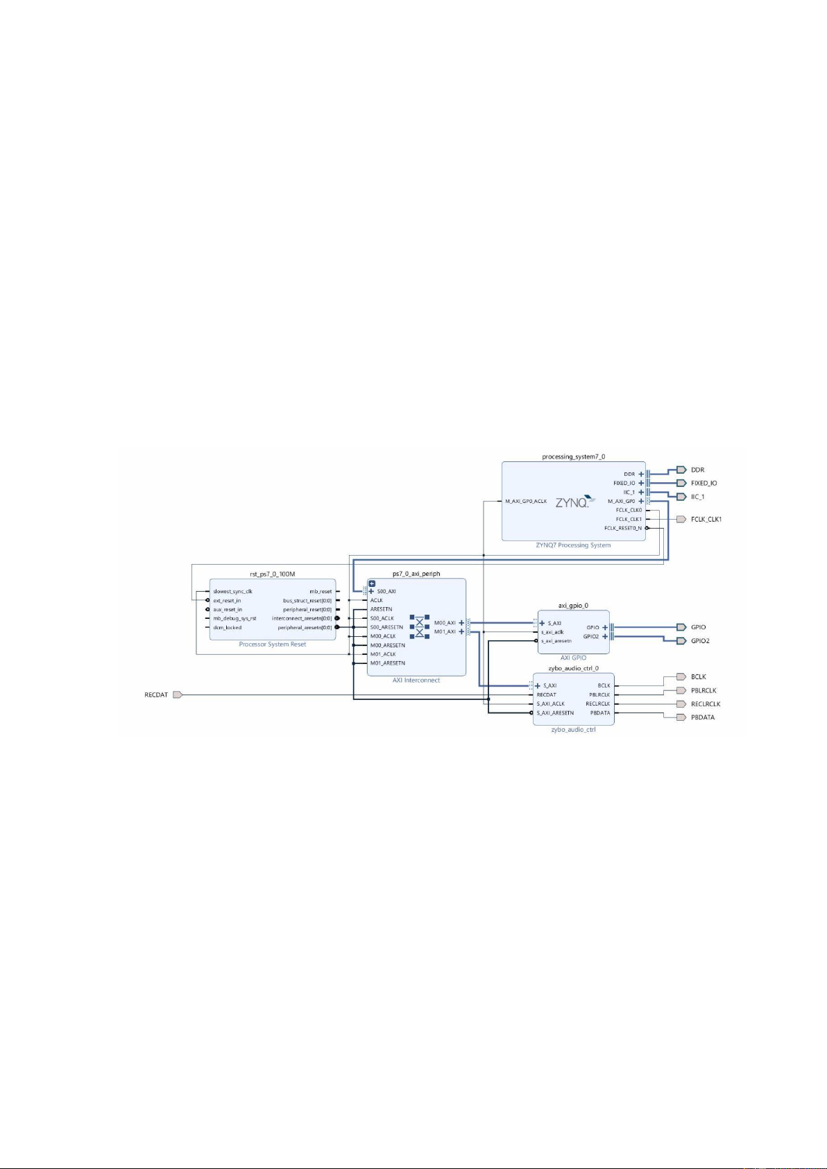
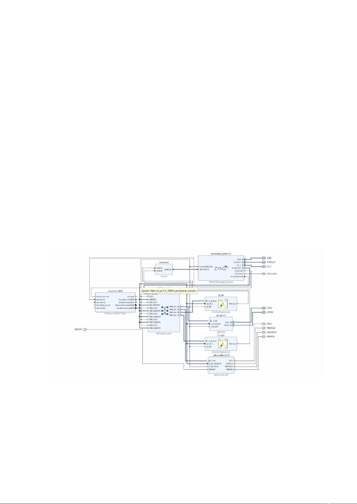
The script will be run and the initial system, shown below, will be created.
Figure 10: Block design made for Pynq
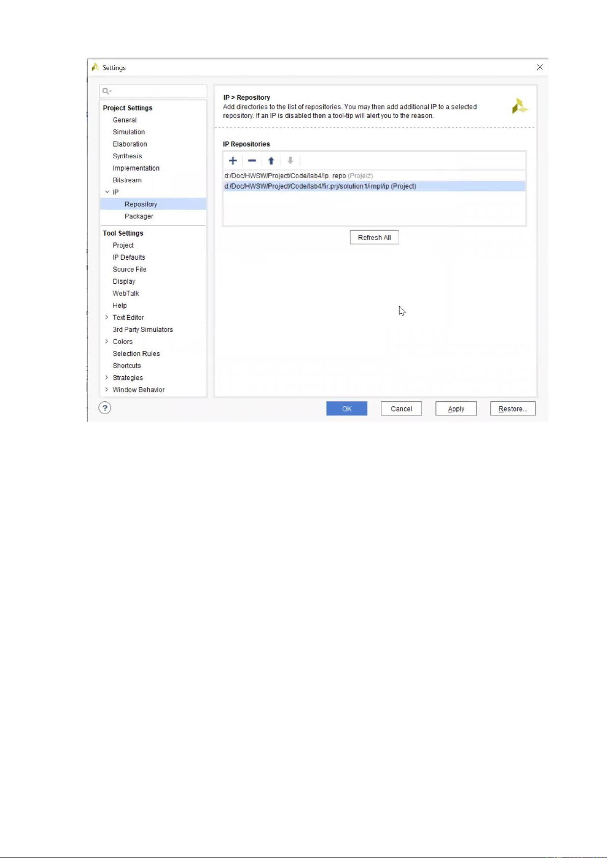
Add the HLS IP to the IP Catalog
1. Select Flow Navigator > Project Manager > Settings
2. Expand IP > Repository in the left pane.
3. Click the + button (The lab4/ip_repo directory has already been added). Browse to
{labs}\lab4\fir.prj\solution1\impl\ip and click Select.
The directory will be scanned and added in the IP Repositories window, and one IP entry will be detected. 4. Click OK. lOMoARcPSD| 36625228
Figure 11: Setting path to IP Repositories
5. Click OK to accept the settings
Instantiate fir_top core twice, one for each side channel, into the processing
system naming the instances as fir_left and fir_right.
1. Click the Add IP icon (+) and search for Fir in the catalog by typing Fir and double-
click on the Fir entry to add an instance.
Notice that the added IP has HLS logo in it indicating that this was created by Vivado HLS.
2. Select the added instance in the diagram, and change its instance name to fir_left
by typing it in the Name field of the Block Properties form in the left.
3. Similarly, add another instance of the HLS IP, and naming it fir_right.
4. Click on Run Connection Automation, and select All Automation.
5. Click on /fir_left/s_axi_fir_io and /fir_right/s_axi_fir_io. and verify that they will
both be connected to the M_AXI_GP0, and click OK.
Enable the PS-PL Interrupt ports > IRQ_F2P ports. Add an instance of concat
IP with two single-bit input ports. Connect input ports to the interrupt ports of the lOMoARcPSD| 36625228
two FIR instances and the output port to the IRQ_F2P port of the
processing_system7_0 instance.
1. Double-click on the processing_system7_0 instance to open the re-customization form.
2. Select the Interrupt entry in the left pane, click on the Fabric Interrupts check box in the right.
3. Expand the Fabric Interrupts > PL-PS Interrupt Ports > IRQ_F2P entry in the
right, and click the check-box of IRQ_F2P[15:0]. 4. Click OK.
5. Add an instance of the concat IP.
6. Connect the interrupt port of each of the FIR instances to the two input ports of the xlconcat_0 instance.
7. Connect the output port of the xlconcat_0 instance to the IRQ_F2P port of the
processing_system7_0 instance.
At this stage the design should look like shown below (you may have to click the regenerate button).
Figure 12: Generated design after IRQ_F2P interface enabled
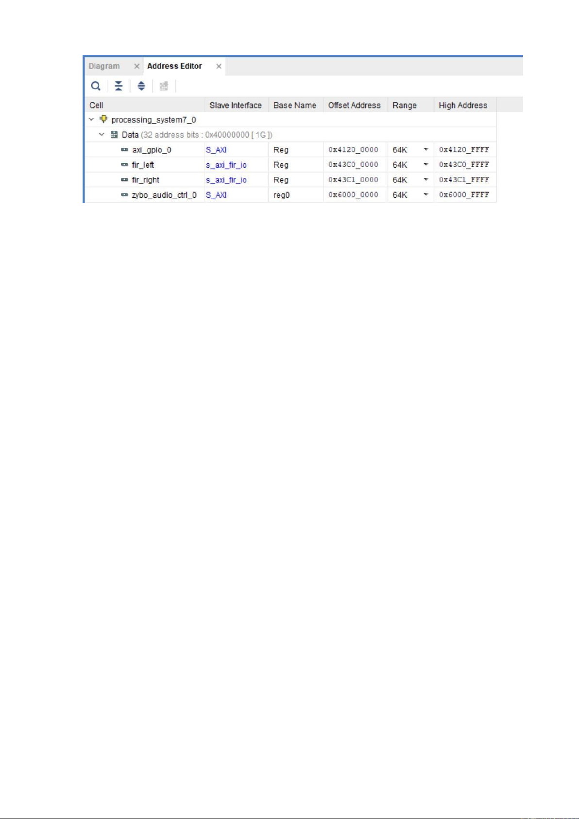
Verify addresses and validate the design. Generate the system_wrapper file,
and add the provided Xilinx Design Constraints (XDC). 1.
Click on the Address Editor, and expand the processing_system7_0 > Data if necessary.
The generated address map should look like as shown below. lOMoARcPSD| 36625228
Figure 13: Generated address map 2.
Run Design Validation (Tools > Validate Design) and verify there are no errors
3. In the sources view, right-click on the block diagram file, system.bd, and select
Create HDL Wrapper to update the HDL wrapper file. When prompted, click OK with
the Let Vivado manage wrapper and auto-update option.
4. Click Add Sources in the Flow Navigator
pane, select Add or Create
Constraints, and click Next.
5. Click the Add Files button, browse to the {sources}\lab4 folder, select
zybo_audio_constraints.xdc.
6. Click Copy constraints files into project and then click Finish to add the file.
7. Click on the Generate Bitstream in the Flow Navigator to run the synthesis,
implementation, and bitstream generation processes.
8. Click Save, Yes, and OK if prompted to start the process.
9. When the bit generation is completed, a selection box will be displayed with Open
Implemented Design option selected. Click Cancel.
3.8. Export to SDK and create Application Project
Export the hardware along with the generated bitstream to SDK.
1. Select File > Export > Export Hardware…
2. Make sure that Include Bitstream option is selected and click OK, leaving the target
directory set to local project directory.
3. Select File > Launch SDK 4. Click OK.
5. In SDK, select File > New > Board Support Package.
6. Click Finish with the default settings (with standalone operating system). lOMoARcPSD| 36625228
This will open the Software Platform Settings form showing the OS and libraries selections.
7. Click OK to accept the default settings, as we want to create a standalone_bsp_0
software platform project without requiring any additional libraries support.
The library generator will run in the background and will create xparameters.h file in the
{labs}\lab4\audio\audio.sdk\standalone_bsp_0\ps7_cortexa9_0\include directory.
8. Select File > New > Application Project.
9. Enter TestApp as the Project Name, and for Board Support Package, choose Use
Existing (standalone_bsp should be the only option)
10. Click Next, select Empty Application and click Finish
11. Select TestApp in the project view, right-click the src folder, and select Import
12. Expand General category and double-click on File System.
13. Browse to {sources}\lab4 folder and click OK.
14. Select both zybo_testapp.c and zybo_audio.h and click Finish to add the file to the project.
The program should compile successfully.
3.9. Verify the Design in Hardware
Connect a micro-usb cable between a PC and the JTAG port of the board.
Connect an audio patch cable between the Line In jack and the speaker
(headphone) out jack of a PC. Connect a headphone to the Line Out jack on the
board. Power On the board.
1. Connect a micro-usb cable between a PC and the JTAG port of the board.
2. Connect an audio patch cable between the Line In jack and the speaker out (headphone) jack of a PC.
3. Connect a headphone to the HP+MIC jack on board. Power ON the board.
4. Select Xilinx > Program FPGA.
5. Make sure that the system_wrapper.bit bitstream is selected and the BMM file field is blank. 6. Click Program. This will configure the FPGA. lOMoARcPSD| 36625228
7. Double-click corrupted_music_4KHz.wav or some other wave file of interest to
play it using the installed media player. Place it in the continuous play mode.
8. Right-click on the TestApp in the Project Explorer pane and select Run As >
Launch On Hardware (System Debugger).
The program will be downloaded and run. If you want to listen to corrupted signal
then set the SW0 OFF. To listened the filtered signal set the SW0 ON.
9. When done, power OFF the board.
10. Exit SDK and Vivado using File > Exit. lOMoARcPSD| 36625228 PART 4. CONCLUSION
You used the INTERFACE directive to create an IP-XACT adapter in this lab.
During the implementation phase, you created the IP-XACT adapter. You then used IP
Integrator to create a processor system, integrate the generated IP-XACT adapter, and
test the system with the provided application. lOMoARcPSD| 36625228 REFERENCE
1. “Creating a Processor System Lab”,https://github.com/xupgit/High-Level-
Synthesis-Flow-on-Zynq-using-Vivado-HLS/bl ob/master/Lab4.md
2. Vivado Board Files for Digilent FPGA Boards,
https://github.com/Digilent/vivado-boards
Tài liệu liên quan:
-

Creating a processorsystem | Môn Hardware/Software Codesign - Đại học Sư phạm Kỹ thuật Thành phố Hồ Chí Minh
170 85 -

Báo cáo dự án cuối kỳ | Môn Hardware/Software Codesign - Đại học Sư phạm Kỹ thuật Thành phố Hồ Chí Minh
149 75 -
Đề cương Môn Hardware/Software Codesign | Đại học Sư phạm Kỹ thuật Thành phố Hồ Chí Minh
125 63 -

Competitive Programming X-Sum Problem Solution | Môn Hardware/Software Codesign - Đại học Sư phạm Kỹ thuật Thành phố Hồ Chí Minh
114 57 -

Design Project Report Template for Electronics Engineering | Môn Hardware/Software Codesign - Đại học Sư phạm Kỹ thuật Thành phố Hồ Chí Minh
131 66