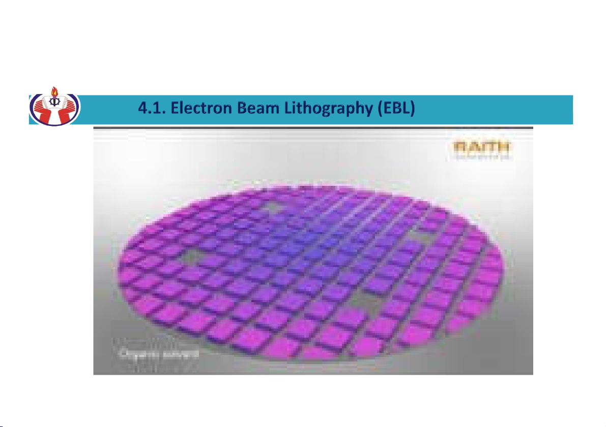
Chapter 4: Electron Beam Lithography Focus Ion Beam Machining | Bài giảng môn công nghệ chế tạo máy Trường đại học sư phạm kỹ thuật TP. Hồ Chí Minh
Mechanically deform a thermoplastic resist on the surface of a substrate in preparation for etching; Transfers a very thin layer of the substance onto the substrate surface in the pattern. EX: Transfer a thin film of thiols (a family of organic compounds derived from hydrogen sulfide) onto a gold surface; Light source;Light-436nm~157nm near UV, DUV to EUV (Optical lithography). Tài liệu giúp bạn tham khảo, ôn tập và đạt kết quả cao. Mời bạn đọc đón xem!
Môn: Công nghệ chế tạo máy 15 tài liệu
Trường: Trường Đại học Sư phạm Kỹ thuật Thành phố Hồ Chí Minh 4.3 K tài liệu
Tác giả:
Preview text:
Lecturer: Dr. Phan Quoc Bao MAC A H C I H N I ER N Y ER Y MAN A U N FACT C UR T I UR N I G N G TECH C N H OL O OG O Y Y DEPA EP R A T R M T EN M T EN JULY 6, 2022 • Beam of electron Electron-beam Lithography Optical Lithography X-ray (Photolithography) Lithography • UV light • X-rays •
EUV (extreme untraviolet) Lithographic techniques Ion Beam Lithography Micro-Nano Imprinting Lithography •
Mechanically deform a thermoplastic resist on the surface of a substrate in preparation for etching •
Transfers a very thin layer of the substance onto the substrate surface in the pattern
EX: Transfer a thin film of thiols (a family of organic compounds derived from hydrogen sulfide) onto a gold surface 2 • Light source
Light-436nm~157nm near UV, DUV to EUV (Optical lithography) X-ray 13nm~0.4nm (X-ray lithography)
Electron beam 10keV~100keV, (Electron beam lithography)
Ion beam 50keV~200keV, (Focus ion beam lithography) • Light source wavelength • Feature Size
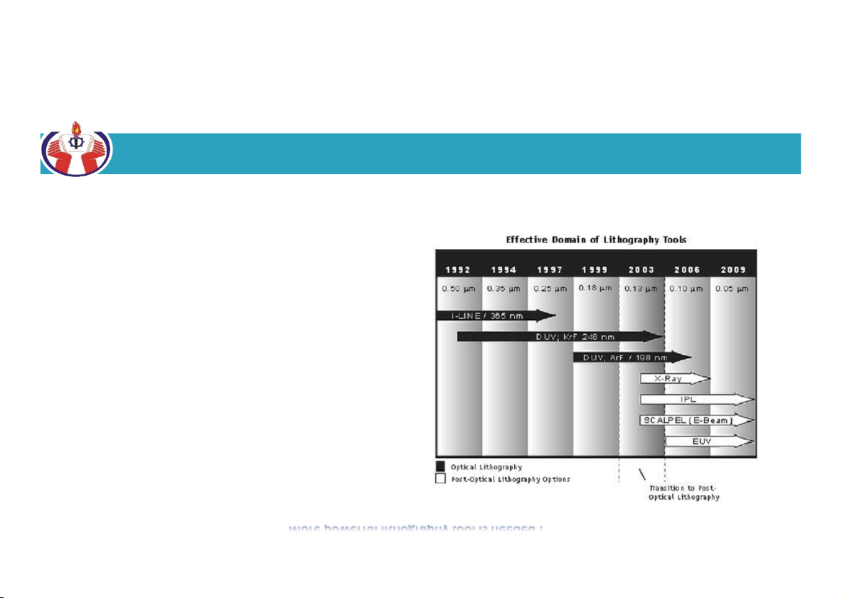
More powerful lithography tool is needed ! 3
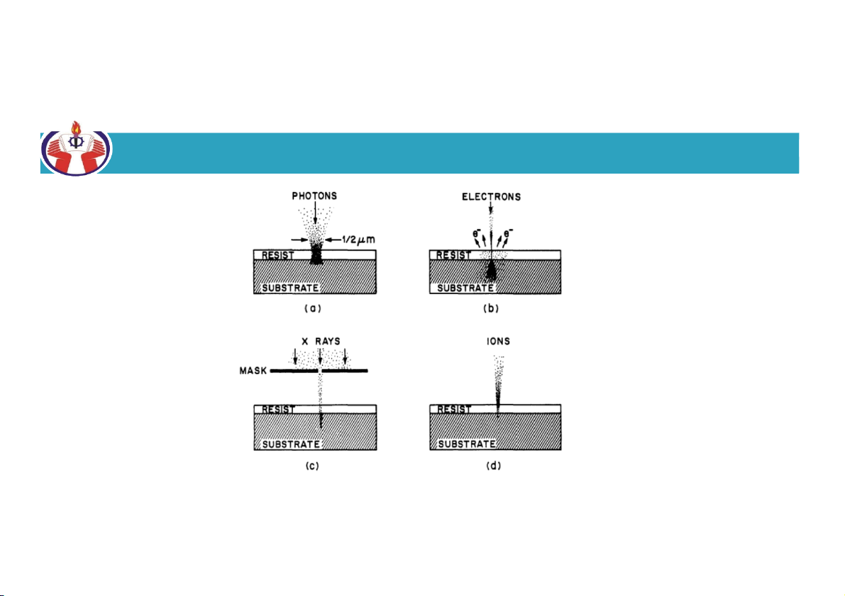
Types of lithographic methods.
(a) Optical lithography. (b) Electron lithography. (c) X-ray lithography. (d) Ion lithography 4
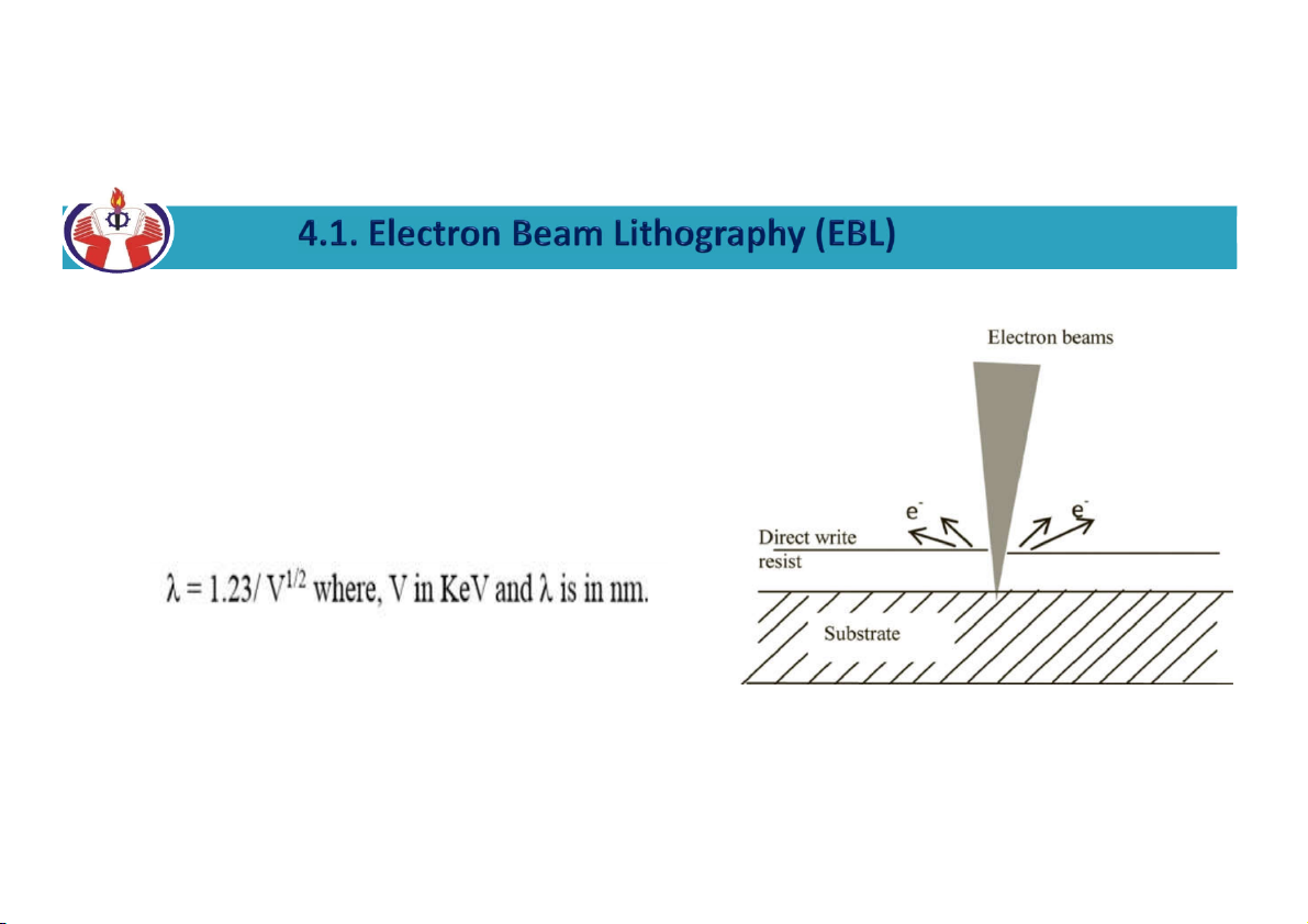
EBL: using accelerated electrons instead of photons. Like
photons, electron has also wave nature.
When electrons are accelerated through a potential V, wavelength is given by:
When V=10keV, λ=0.0123nm which is much smaller than the wavelength of UY light. The electron
beam lithography pattern can be transferred directly on the wafer without mask. 5
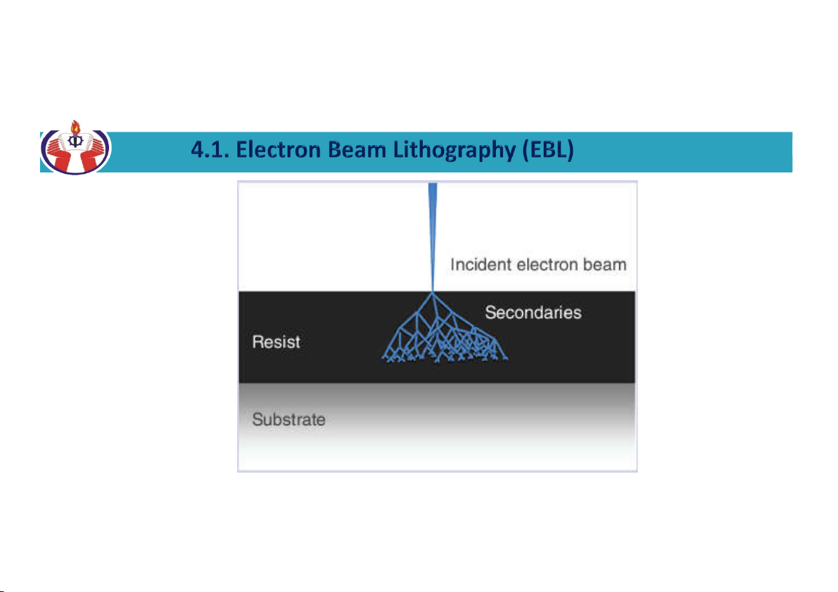
Collision of electrons with the substrate causes random scattering and
back scattering electron generation and also secondary electrons. 6 Schematic
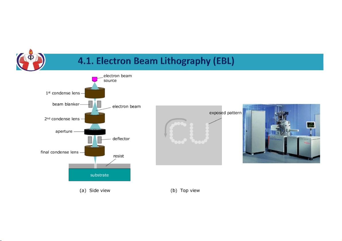
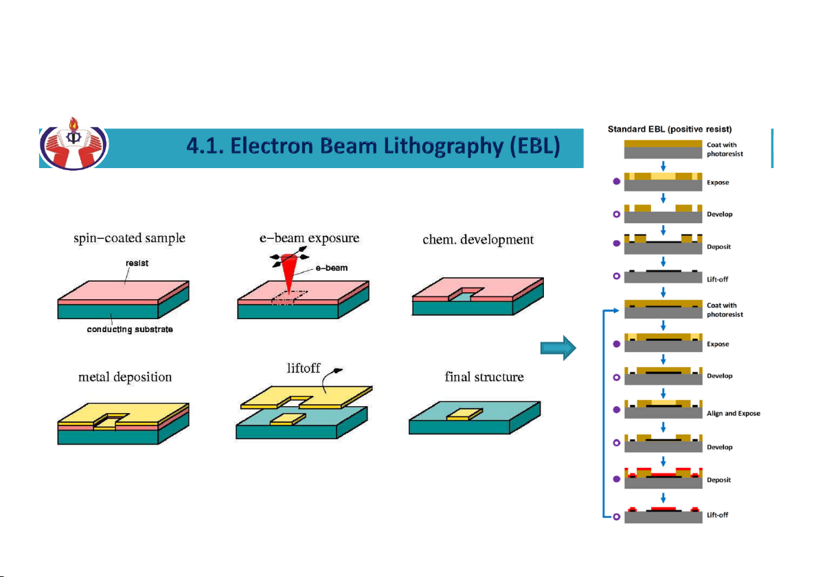
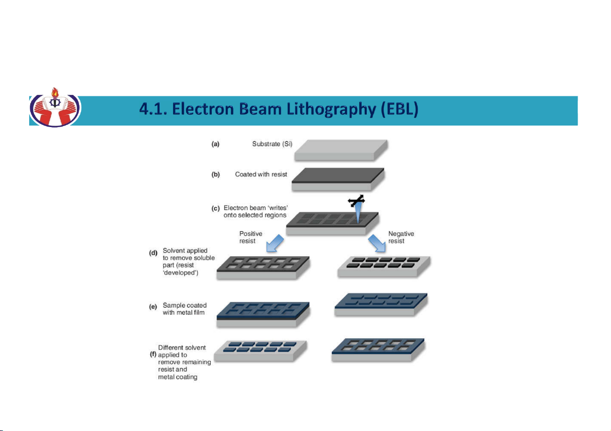
Electron beam is focused on a resist film to create a pattern by exposing dot by dot:
(a) side view of the lithography setup; (b) top view of the exposed pattern by a serial writing 7
E-beam can be directed to expose only certain regions of the wafer surface, thus eliminating the need for a mask.
High-quality electron-beam systems are expensive.
Time-consuming sequential nature of the exposure method, production rates are low compared
with the mask techniques of optical lithography.
E-beam tends to be limited to small production quantities. High maintenance cost
E-beam techniques are widely used for making the masks in UV lithography 8 9
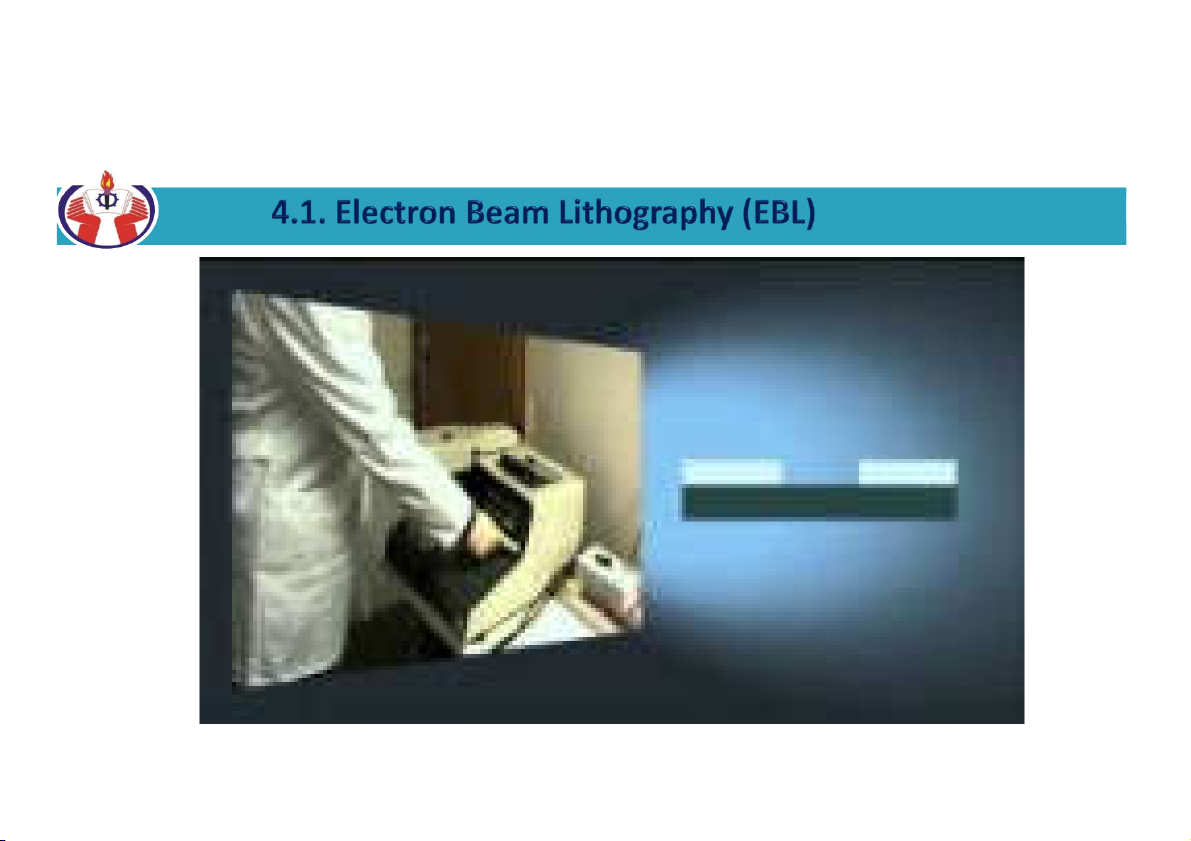
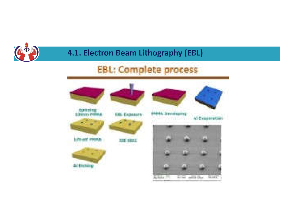
https://www.youtube.com/watch?v=PWV9pvdRBNY EBL Processes
Positive Resist & Negative Resist 11
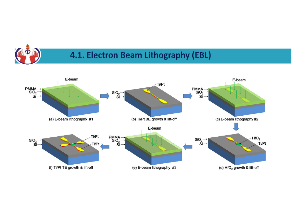
Resistive switching memories (RRAMs) used in cell structure, switching speed, operation power, and fabrication process
Fabrication procedure for the crossbar array based on metal nanowire arrays
Each layer such as the bottom electrode, the resistive switching layer and the top electrode, an e-beam lithography
step, a film deposition step, and a lift-off step are used 12
https://www.youtube.com/watch?v=25AsHRgBJDM 13 14
https://www.youtube.com/watch?v=dw9IvpilfUo 15
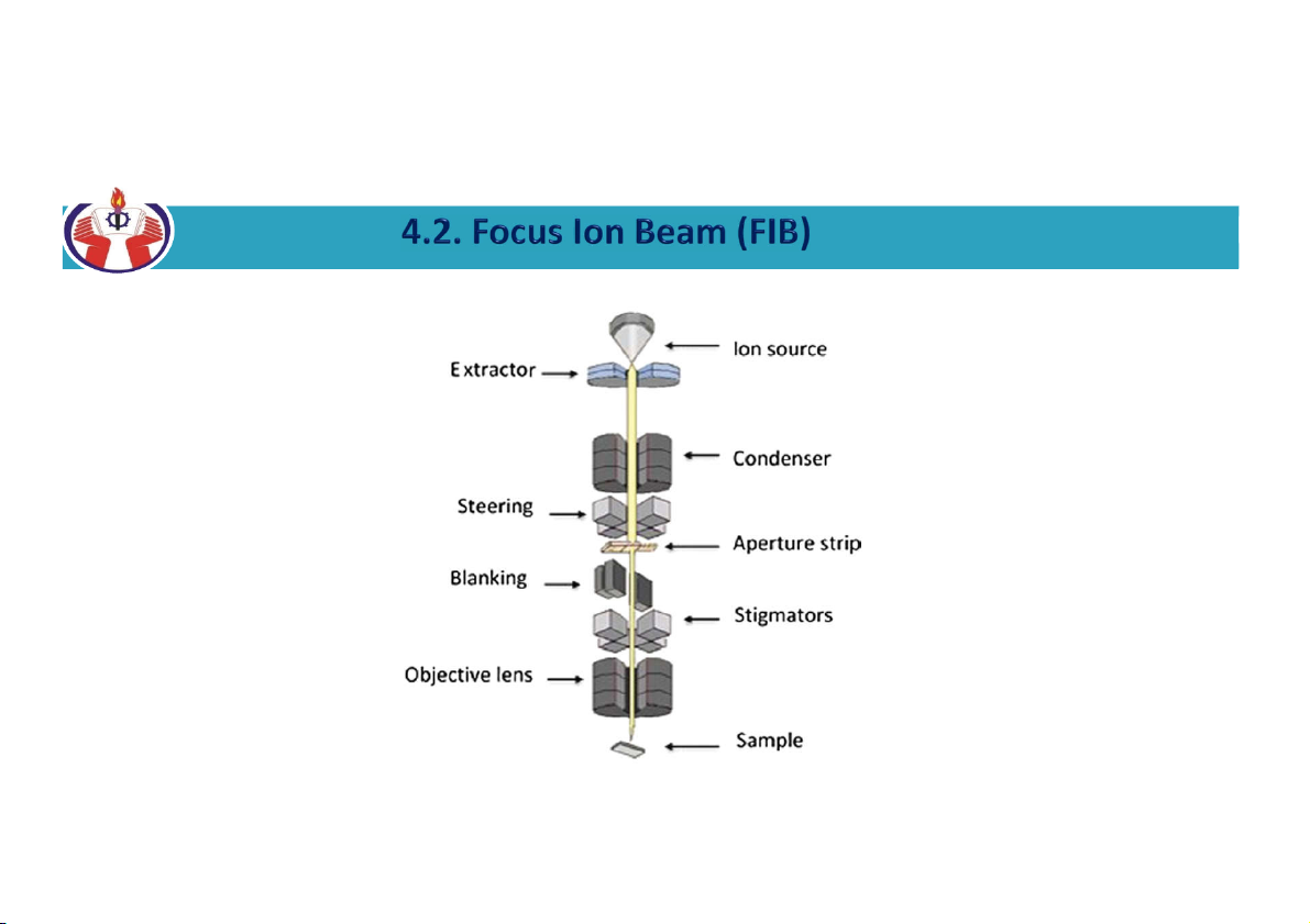
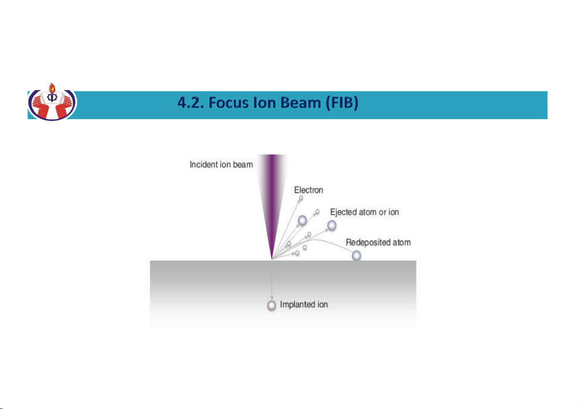
The internal component of a focused ion beam system 16 17 18
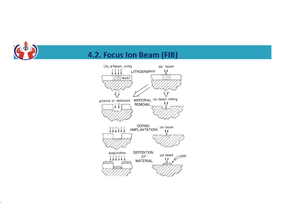
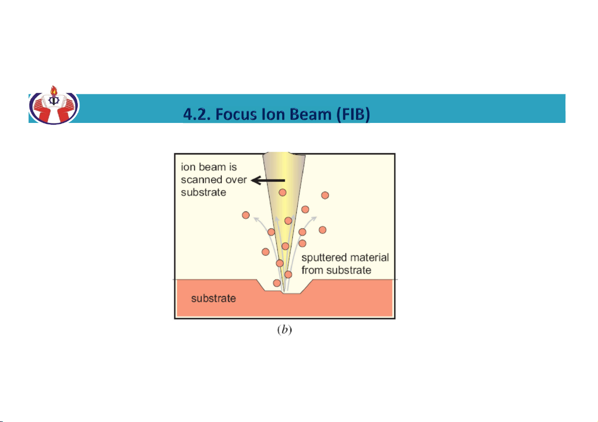
FIBs can be used for milling, imaging and deposition of materials (Sputtering Process)
Manufacture: - Atomic force microscopy tips
- Nanopillar fabrication for mechanical testing
- Cross-sectioning and failure investigation of integrated circuits
- Nanostructure fabrication for devices and sensors Sputtering Process
The removal of sample material is achieved using a high ion current beam.
Tài liệu liên quan:
-
Sổ tay Công nghệ chế tạo máy Tập 1 | Trường Đại học Sư phạm Kỹ thuật Thành phố Hồ Chí Minh
42 21 -

Đề thi cuối học kỳ 1 năm học 2020-2021 môn Vật liệu học | Trường Đại học Sư phạm Kỹ thuật Thành phố Hồ Chí Minh
42 21 -
Đề thi HK1Công nghệ chế tạo máy năm 2024 - 2025 | Trường Đại học Sư phạm kỹ thuật, thành phố Hồ Chí Minh
32 16 -
Báo cáo thực tập tốt nghiệp công ty TNHH cơ khí và thương mại Nhật Long | Nghành công nghệ chế tạo máy Trường đại học sư phạm kỹ thuật TP. Hồ Chí Minh
724 362 -
Thiết kế lò sấy gỗ | Tiểu luận môn Công nghệ chế tạo máy Trường đại học sư phạm kỹ thuật TP. Hồ Chí Minh
366 183