Chapter 5 - Cache Memory Concepts and Design Principles | Môn Computer Architecture and Organization Lab - Đại học Sư phạm Kỹ thuật Thành phố Hồ Chí Minh
Cache memoryis designed to combine the memory access time of expensive, high-speed memory combined with the large memory size of less expensive, lower-speed memory. Tài liệu được sưu tầm gồm 46 trang, giúp bạn ôn tập tốt hơn. Mời các bạn đón xem.
Môn: Computer Architecture and Organization Lab (COOL325364E) 10 tài liệu
Trường: Trường Đại học Sư phạm Kỹ thuật Thành phố Hồ Chí Minh 4.4 K tài liệu
Tác giả:


Preview text:
lOMoAR cPSD| 58605085 Chapter 5 Cache Memory
5.1 Cache Memory Principles 5.2 Elements of Cache Design Cache Addresses Cache Size
Logical Cache Organization Replacement Algorithms Write Policy Line Size Number of Caches Inclusion Policy
5.3 Intel x86 Cache Organization 5.4 The IBM z13 Cache Organization 5.5 Cache Performance Models Cache Timing Model
Design Option for Improving Performance
5.6 Key Terms, Review Questions, and Problems Learning Objectives
After studying this chapter, you should be able to:
Discuss the key elements of cache design.
Distinguish among direct mapping, associative mapping, and set-associative mapping.
Understand the principles of content-addressable memory.
Explain the reasons for using multiple levels of cache.
Understand the performance implications of cache design decisions.
With the exception of smaller embedded systems, all modern computer systems
employ one or more layers of cache memory. Cache memory is vital to achieving
high performance. This chapter begins with an overview of the basic principles of
cache memory, then looks in detail at the key elements of cache design. This is
followed by a discussion of the cache structures used in the Intel x86 family and
the IBM z13 mainframe system. Finally, the chapter introduces some
straightforward performance models that provide insight into cache design. 5.1 Cache Memory Principles
Cache memory is designed to combine the memory access time of expensive, high-speed
memory combined with the large memory size of less expensive, lower-speed memory. The concept
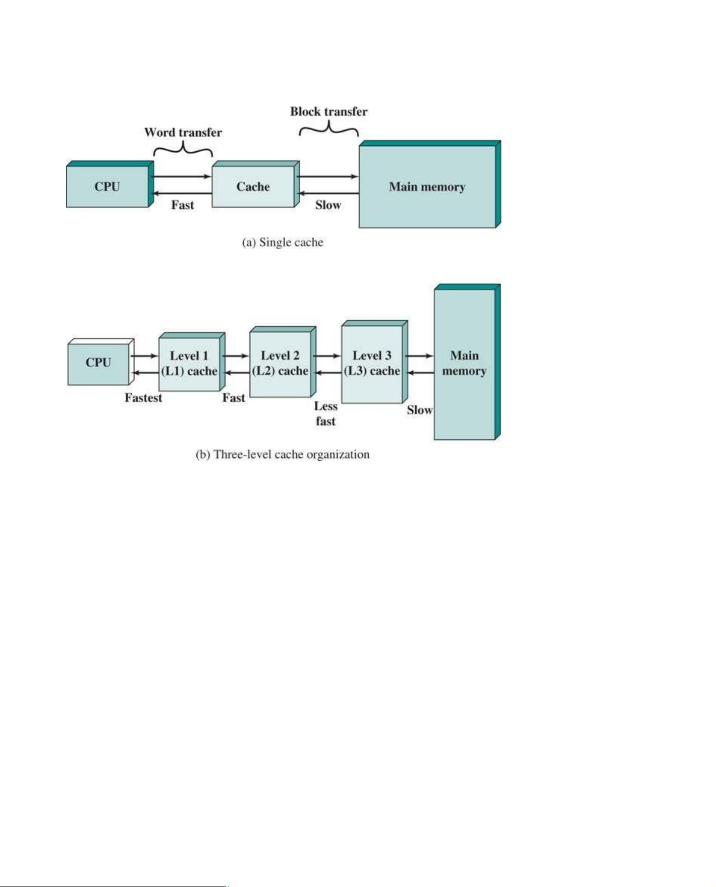
is illustrated in Figure 5.1a. There is a relatively large and slow main memory together with a
smaller, faster cache memory. The cache contains a copy of portions of the main memory. When the
processor attempts to read a word of memory, a check is made to determine if the word is in the
cache. If so, the word is delivered to the processor. If not, a block of main memory, consisting of lOMoAR cPSD| 58605085
some fixed number of words, is read into the cache and then the word is delivered to the processor.
Because of the phenomenon of locality of reference, when a block of data is fetched into the cache
to satisfy a single memory reference, it is likely that there will be future references to that same
memory location or to other words in the block.
Figure 5.1 Cache and Main Memory
Figure 5.1b depicts the use of multiple levels of cache. The L2 cache is slower and typically larger
than the L1 cache, and the L3 cache is slower and typically larger than the L2 cache.
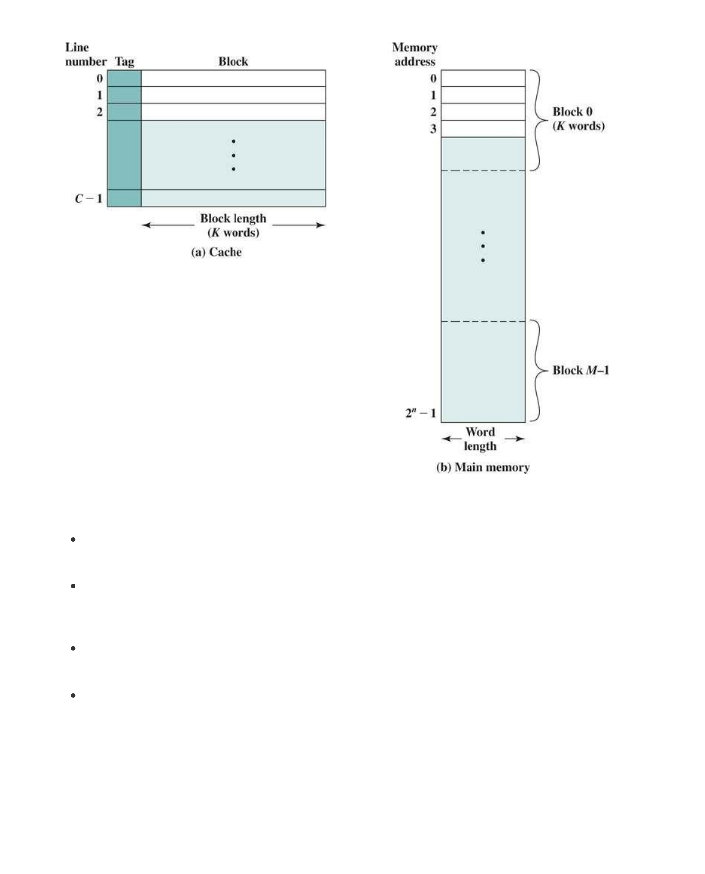
Figure 5.2 depicts the structure of a cache/main-memory system. Several terms are introduced: lOMoAR cPSD| 58605085
Figure 5.2 Cache/Main Memory Structure
Block: The minimum unit of transfer between cache and main memory. In most of the literature,
the term block refers both to the unit of data transferred and to the physical location in main memory or cache.
Frame: To distinguish between the data transferred and the chunk of physical memory, the term
frame, or block frame, is sometimes used with reference to caches. Some texts and some
literature use the term with reference to the cache and some with reference to main memory. It
use is not necessary for purposes of this text.
Line: A portion of cache memory capable of holding one block, so-called because it is usually
drawn as a horizontal object (i.e., all bytes of the line are typically drawn in one row). A line also includes control information.
Tag: A portion of a cache line that is used for addressing purposes, as explained subsequently. A
cache line may also include other control bits, as will be shown.
Main memory consists of up to 2n addressable words, with each word having a unique n-bit address.
For mapping purposes, this memory is considered to consist of a number of fixed-length blocks of K
words each. That is, there are M =2n/K blocks in main memory. The cache consists of m lines. Each
line contains K words, plus a tag. Each line also includes control bits (not shown), such as a bit to
indicate whether the line has been modified since being loaded into the cache. The length of a line,
not including tag and control bits, is the line size. That is, the term line size refers to the number of lOMoAR cPSD| 58605085
data bytes, or block size, contained in a line. They may be as small as 32 bits, with each “word”
being a single byte; in this case the line size is 4 bytes. The number of lines is considerably less than
the number of main memory blocks (m ≪M). At any time, some subset of the blocks of memory
resides in lines in the cache. If a word in a block of memory is read, that block is transferred to one
of the lines of the cache. Because there are more blocks than lines, an individual line cannot be
uniquely and permanently dedicated to a particular block. Thus, each line includes a tag that
identifies which particular block is currently being stored. The tag is usually a portion of the main
memory address, as described later in this section.
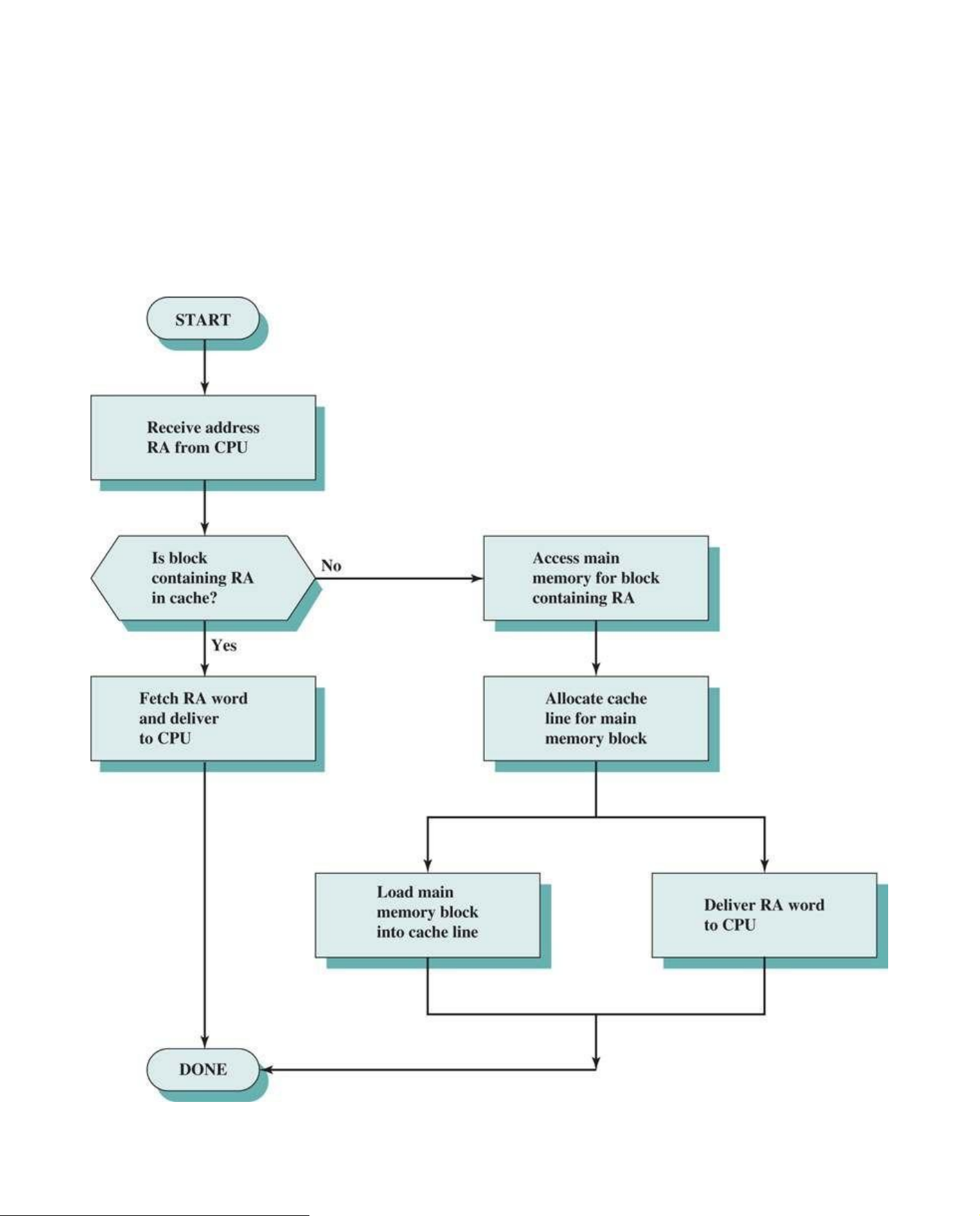
Figure 5.3 illustrates the read operation. The processor generates the read address (RA) of a word
to be read. If the word is contained in the cache (cache hit), it is delivered to the processor. lOMoAR cPSD| 58605085
Figure 5.3 Cache Read Operation
If a cache miss occurs, two things must be accomplished: the block containing the word must be
loaded in to the cache, and the word must be delivered to the processor. When a block is brought
into a cache in the event of a miss, the block is generally not transferred in a single event. Typically,
the transfer size between cache and main memory is less than the line size, with 128 bytes being a
typical line size and a cache-main memory transfer size of 64 bits (2 bytes). To improve
performance, the critical word first technique is commonly used. When there is a cache miss, the
hardware requests the missed word first from memory and sends it to the processor as soon as it
arrives. This enables the processor to continue execution while filling the rest of the words in the
block. Figure 5.3 shows these last two operations occurring in parallel and reflects the organization
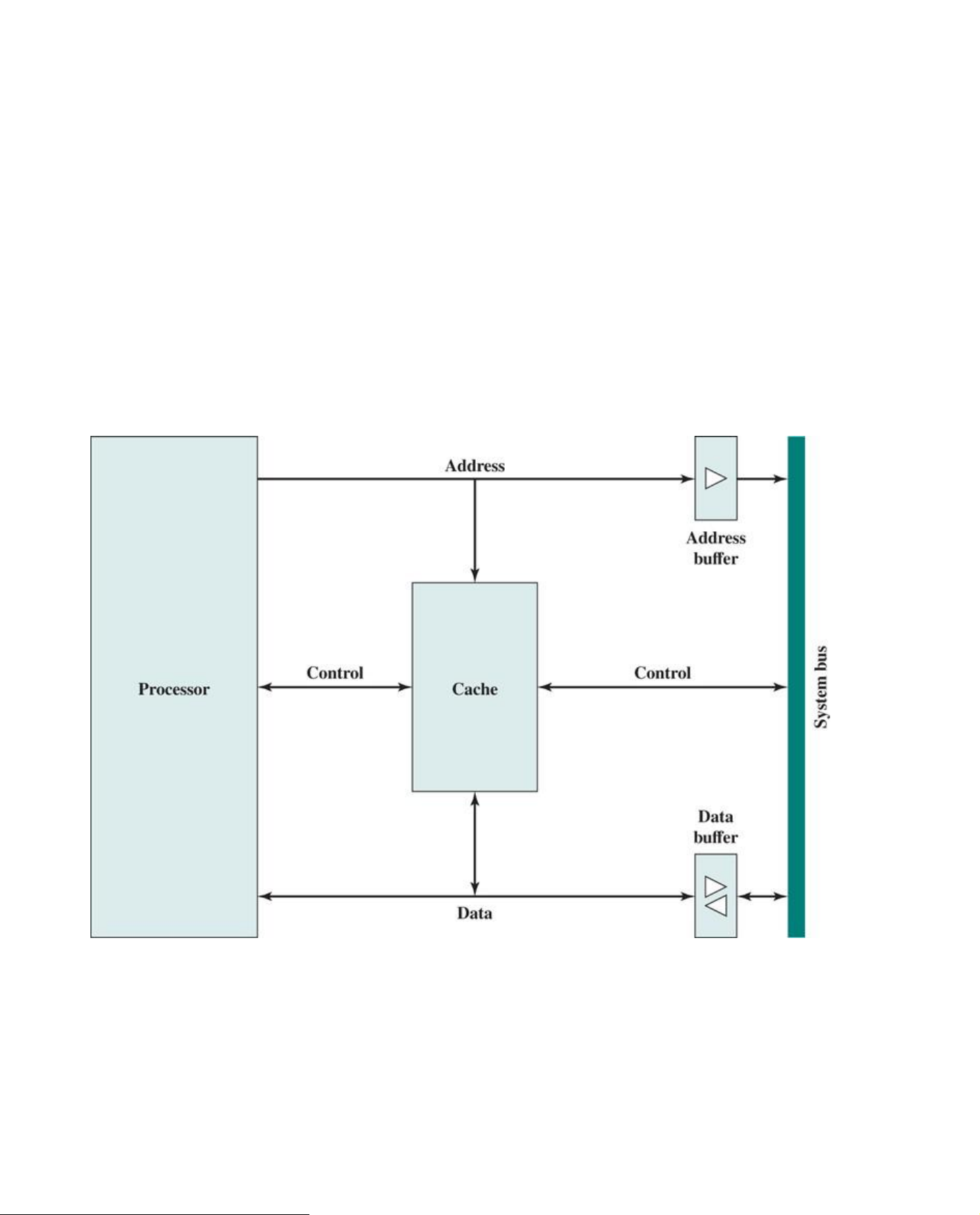
shown in Figure 5.4, which is typical of contemporary cache organizations. In this organization, the
cache connects to the processor via data, control, and address lines. The data and address lines
also attach to data and address buffers, which attach to a system bus from which main memory is
reached. When a cache hit occurs, the data and address buffers are disabled and communication is
only between processor and cache, with no system bus traffic. When a cache miss occurs, the
desired address is loaded onto the system bus and the data are returned through the data buffer to
both the cache and the processor.
Figure 5.4 Typical Cache Organization 5.2 Elements of Cache Design
This section provides an overview of cache design parameters and reports some typical results. We
occasionally refer to the use of caches in high-performance computing (HPC) . HPC deals with
supercomputers and their software, especially for scientific applications that involve large amounts
of data, vector and matrix computation, and the use of parallel algorithms. Cache design for HPC is
quite different than for other hardware platforms and applications. Indeed, many researchers have
found that HPC applications perform poorly on computer architectures that employ caches [BAIL93]. lOMoAR cPSD| 58605085
Other researchers have since shown that a cache hierarchy can be useful in improving performance
if the application software is tuned to exploit the cache [WANG99, PRES01].4 4 For a general
discussion of HPC, see [DOWD98].
Although there are a large number of cache implementations, there are a few basic design elements
that serve to classify and differentiate cache architectures. Table 5.1 lists key elements.
Table 5.1 Elements of Cache Design Write Policy Cache Addresses Write through Logical Write back Physical Line Size Cache Size Number of Caches Mapping Function Single or two level Direct Unified or split Associative Set associative Replacement Algorithm Least recently used (LRU) First in first out (FIFO) Least frequently used (LFU) Random Cache Addresses
Almost all nonembedded processors, and many embedded processors, support virtual memory, a
concept discussed in Chapter 9. In essence, virtual memory is a facility that allows programs to
address memory from a logical point of view, without regard to the amount of main memory
physically available. When virtual memory is used, the address fields of machine instructions
contain virtual addresses. For reads to and writes from main memory, a hardware memory
management unit (MMU) translates each virtual address into a physical address in main memory.
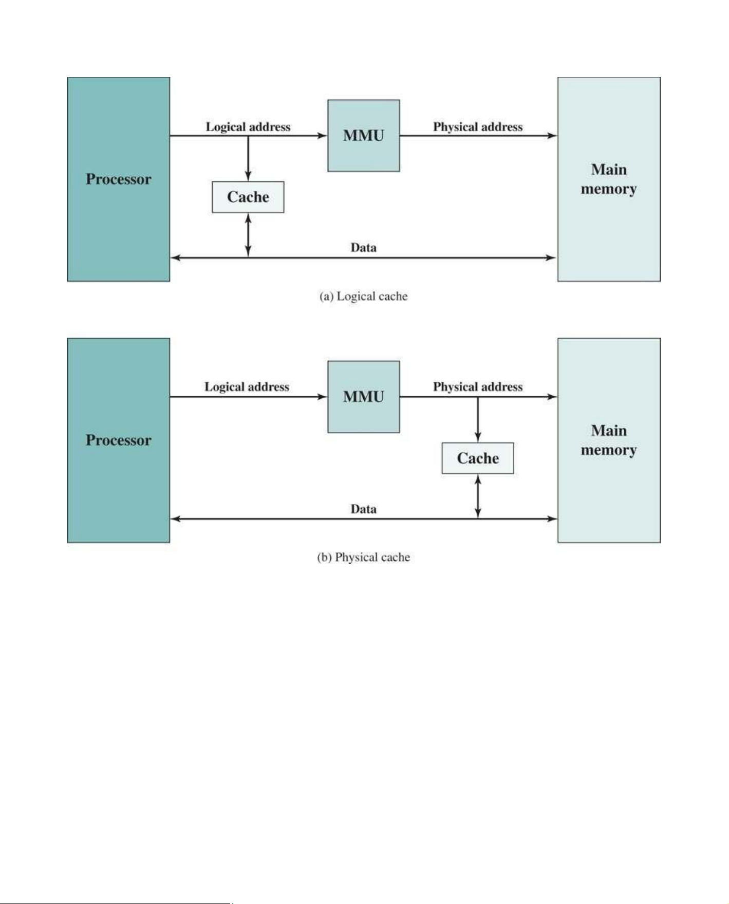
When virtual addresses are used, the system designer may choose to place the cache between the
processor and the MMU or between the MMU and main memory (Figure 5.5). A logical cache, also
known as a virtual cache, stores data using virtual addresses. The processor accesses the cache lOMoAR cPSD| 58605085
directly, without going through the MMU. A physical cache stores data using main memory physical addresses.
Figure 5.5 Logical and Physical Caches
One obvious advantage of the logical cache is that cache access speed is faster than for a physical
cache, because the cache can respond before the MMU performs an address translation. The
disadvantage has to do with the fact that most virtual memory systems supply each application with
the same virtual memory address space. That is, each application sees a virtual memory that starts
at address 0. Thus, the same virtual address in two different applications refers to two different physical
addresses. The cache memory must therefore be completely flushed with each application context
switch, or extra bits must be added to each line of the cache to identify which virtual address space this address refers to.
The subject of logical versus physical cache is a complex one, and beyond the scope of this text.
For a more in-depth discussion, see [CEKL97] and [JACO08]. lOMoAR cPSD| 58605085 Cache Size
The second item in Table 5.1, cache size, has already been discussed. We would like the size of the
cache to be small enough so that the overall average cost per bit is close to that of main memory
alone and large enough so that the overall average access time is close to that of the cache alone.
There are several other motivations for minimizing cache size. The larger the cache, the larger the
number of gates involved in addressing the cache. The result is that large caches tend to be slightly
slower than small ones—even when built with the same integrated circuit technology and put in the
same place on a chip and circuit board. The available chip and board area also limits cache size.
Because the performance of the cache is very sensitive to the nature of the workload, it is
impossible to arrive at a single “optimum” cache size. Table 5.2 lists the cache sizes of some current and past processors.
Table 5.2 Cache Sizes of Some Processors Processor Type L1 Cachea L2 cache Year of L3 Introduction Cache IBM 360/85 Mainframe 1968 16 to 32 kB — — PDP-11/70 Minicomputer 1975 1 kB — — IBM 3033 Mainframe 1978 64 kB — — IBM 3090 Mainframe 1985 128 to 256 kB — — Intel 80486 PC 1989 8 kB — — Pentium PC 1993 8 kB/8 kB 256 to 512 kB — PowerPC 620 PC 1996 32 kB/32 kB — — IBM S/390 Mainframe G6 1999 256 kB 8 MB — Pentium 4 PC/server 2000 8 kB/8 kB 256 kB — Itanium PC/server 2001 16 kB/16 kB 96 kB 4 MB Itanium 2 PC/server 2002 32 kB 256 kB 6 MB IBM 36 High-end server POWER5 2003 64 kB 1.9 MB MB CRAY XD-1 Supercomputer 2004 64 kB/64 kB 1MB — IBM 32 PC/server POWER6 2007 64 kB/64 kB 4 MB MB lOMoAR cPSD| 58605085 IBM z10 Mainframe 2008 64 kB/128 kB 3 MB 24-48 MB Workstaton/Server Intel Core i7 2011 6 × 32kB / 32kB 6 × 1.5MB 12 MB EE 990 IBM Mainframe/Server 2011 24 × 64kB / 128kB 24 × 1.5MB 24 MB zEnterprise L3 196 192 MB L4 IBM z13 Mainframe/server 2015 24 × 96kB / 128kB 24 × 2MB / 2MB 64 MB L3 480 MB L4 Workstation/server Intel Core i0- 2017 8 × 32kB / 32kB 8 × 1MB 14 MB 7900X
a Two values separated by a slash refer to instruction and data caches. Logical Cache Organization
Because there are fewer cache lines than main memory blocks, an algorithm is needed for mapping
main memory blocks into cache lines. Further, a means is needed for determining which main
memory block currently occupies a cache line
. The choice of the mapping function dictates how
the cache is logically organized. Three techniques can be used: direct, associative, and set-
associative. We examine each of these in turn. In each case, we look at the general structure and
then a specific example. Table 5.3 provides a summary of key characteristics of the three approaches.
Table 5.3 Cache Access Methods Method Organization
Access using Main Memory Address Mapping of Main Memory Blocks to Cache Sequence of m lines Direct
Line portion of address used to
Each block of main access cache line; Tag portion used Mapped memory maps to to check one unique line of for hit on that line. cache. lOMoAR cPSD| 58605085 Fully Sequence of m lines
Each block of main Tag portion of address used to check Associative memory can map
every line for hit on that line. to any line of cache. Set Sequence of m lines
Line portion of address used to Associative Each block of main organized as v sets
access cache set; Tag portion used to memory maps to
check every line in that set for hit on of k lines each one unique cache that line.
(m = v × k) set.
Example 5.1
For all three cases, the example includes the following elements: The cache can hold 64 kB.
Data are transferred between main memory and the cache in blocks of 4 bytes each. This
means that the cache is organized as 16K = 214 lines of 4 bytes each.
The main memory consists of 16 MB, with each byte directly addressable by a 24-bit address
(224 = 16M). Thus, for mapping purposes, we can consider main memory to consist of 4M blocks of 4 bytes each. Direct Mapping
The simplest technique, known as direct mapping, maps each block of main memory into only one
possible cache line. The mapping is expressed as
i = j modulo m where
i = cache line number j = main memory block number m
= number of lines in the cache
Figure 5.6a shows the mapping for the first m blocks of main memory. Each block of main memory
maps into one unique line of the cache. The next m blocks of main memory map into the cache in
the same fashion; that is, block Bm of main memory maps into line L0 of cache, block Bm +1 maps into line L1, and so on. lOMoAR cPSD| 58605085
Figure 5.6 Mapping from Main Memory to Cache: Direct and Associative
The mapping function is easily implemented using the main memory address. Figure 5.7 illustrates
the general mechanism. For purposes of cache access, each main memory address can be viewed
as consisting of three fields. The least significant w bits identify a unique word or byte within a block
of main memory; in most contemporary machines, the address is at the byte level. The remaining s
bits specify one of the 2s blocks of main memory. The cache logic interprets these s bits as a tag of s
− r bits (most significant portion) and a line field of r bits. This latter field identifies one of the m = 2r
lines of the cache. To summarize, lOMoAR cPSD| 58605085
Figure 5.7 Direct-Mapping Cache Organization
Address length = (s + w ) bits s + w
Number of addressable units = 2 words or bytes w
Block size = line size = 2 words or bytes s + w 2 s
Number of blocks in main memory = w = 2 2 r
Number of lines in cache = m = 2 r + w Size of cache = 2 words or bytes
Size of tag = (s − r ) bits
The effect of this mapping is that blocks of main memory are assigned to lines of the cache as follows: Cache line Main memory blocks assigned s 0
0 , m , 2m , … , 2 − m lOMoAR cPSD| 58605085 s 1
1 , m + 1 , 2m + 1 , … , 2 − m + 1 ⋮ ⋮ ((m − 1)) s m
− 1 , 2m − 1 , 3m − 1 , … , 2 − 1
Thus, the use of a portion of the address as a line number provides a unique mapping of each block
of main memory into the cache. When a block is actually read into its assigned line, it is necessary
to tag the data to distinguish it from other blocks that can fit into that line. The most significant s − r bits serve this purpose.
Figure 5.7 indicates the logical structure of the cache hardware access mechanism. When the
cache hardware is presented with an address from the processor, the Line Number portion of the
address is used to index into the cache. A compare function compares the tag of that line with the
Tag field of the address. If there is a match (hit), an enable signal is sent to a select function, which
uses the Offset field of the address and the Line Number field of the address to read the desired
word or byte from the cache. If there is no match (miss) then the select function is not enabled and
data is accessed from main memory, or the next level of cache. Figure 5.7 illustrates the case in
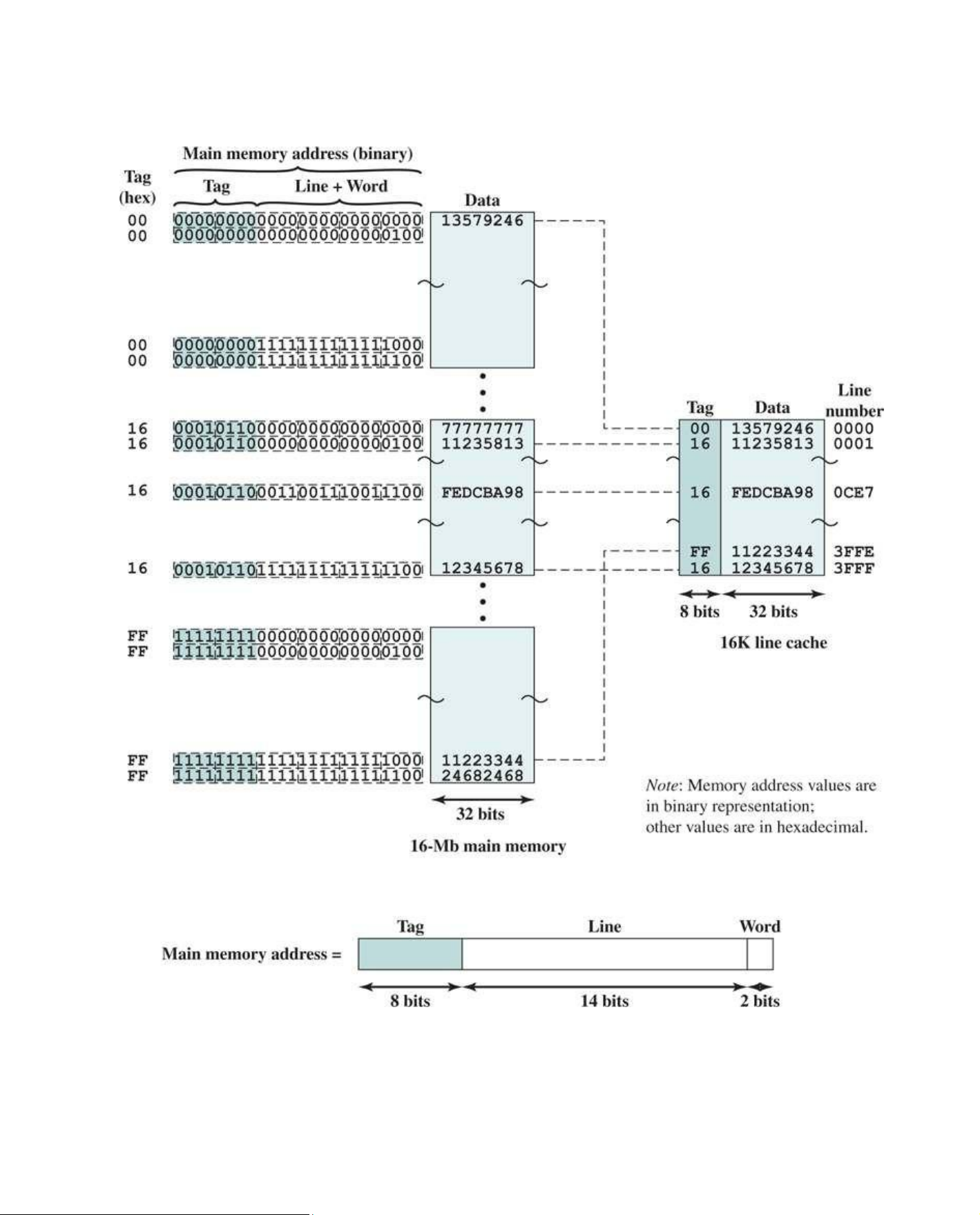
which the line number refers to the third line in the cache and there is a match, as indicated by the heavier arrowed lines. Example 5.1a
Figure 5.8 shows our example system using direct mapping. In the example, 5 m = 16K = 214 and
14 i = jmodulo 2 . The mapping becomes
5 In this and subsequent figures, memory values are represented in hexadecimal notation. See Chapter 9 for
a basic refresher on number systems (decimal, binary, hexadecimal). Cache Line
Starting Memory Address of Block 0 000000, 010000, …, FF0000 1 000004, 010004, …, FF0004 ⋮ ⋮ 14 00FFFC, 01FFFC, …, FFFFFC 2 − 1
Note that no two blocks that map into the same line number have the same tag number. Thus,
blocks with starting addresses 000000, 010000, …, FF0000 have tag numbers 00, 01, …, FF, respectively.
Referring back to Figure 5.3, a read operation works as follows. The cache system is presented
with a 24-bit address. The 14-bit line number is used as an index into the cache to access a
particular line. If the 8-bit tag number matches the tag number currently stored in that line, then the lOMoAR cPSD| 58605085
2-bit word number is used to select one of the 4 bytes in that line. Otherwise, the 22-bit tag-plus-
line field is used to fetch a block from main memory. The actual address that is used for the fetch
is the 22-bit tag-plus-line concatenated with two 0 bits, so that 4 bytes are fetched starting on a block boundary.
Figure 5.8 Direct Mapping Example
The direct mapping technique is simple and inexpensive to implement. Its main disadvantage is that
there is a fixed cache location for any given block. Thus, if a program happens to reference words lOMoAR cPSD| 58605085
repeatedly from two different blocks that map into the same line, then the blocks will be continually
swapped in the cache, and the hit ratio will be low (a phenomenon known as thrashing). Aleksandr Lukin/123RF
Selective Victim Cache Simulator
One approach to lower the miss penalty is to remember what was discarded in case it is needed
again. Since the discarded data has already been fetched, it can be used again at a small cost.
Such recycling is possible using a victim cache. Victim cache was originally proposed as an
approach to reduce the conflict misses of direct mapped caches without affecting its fast access
time. Victim cache is a fully associative cache, whose size is typically 4 to 16 cache lines, residing
between a direct mapped L1 cache and the next level of memory. This concept is explored in Appendix B.
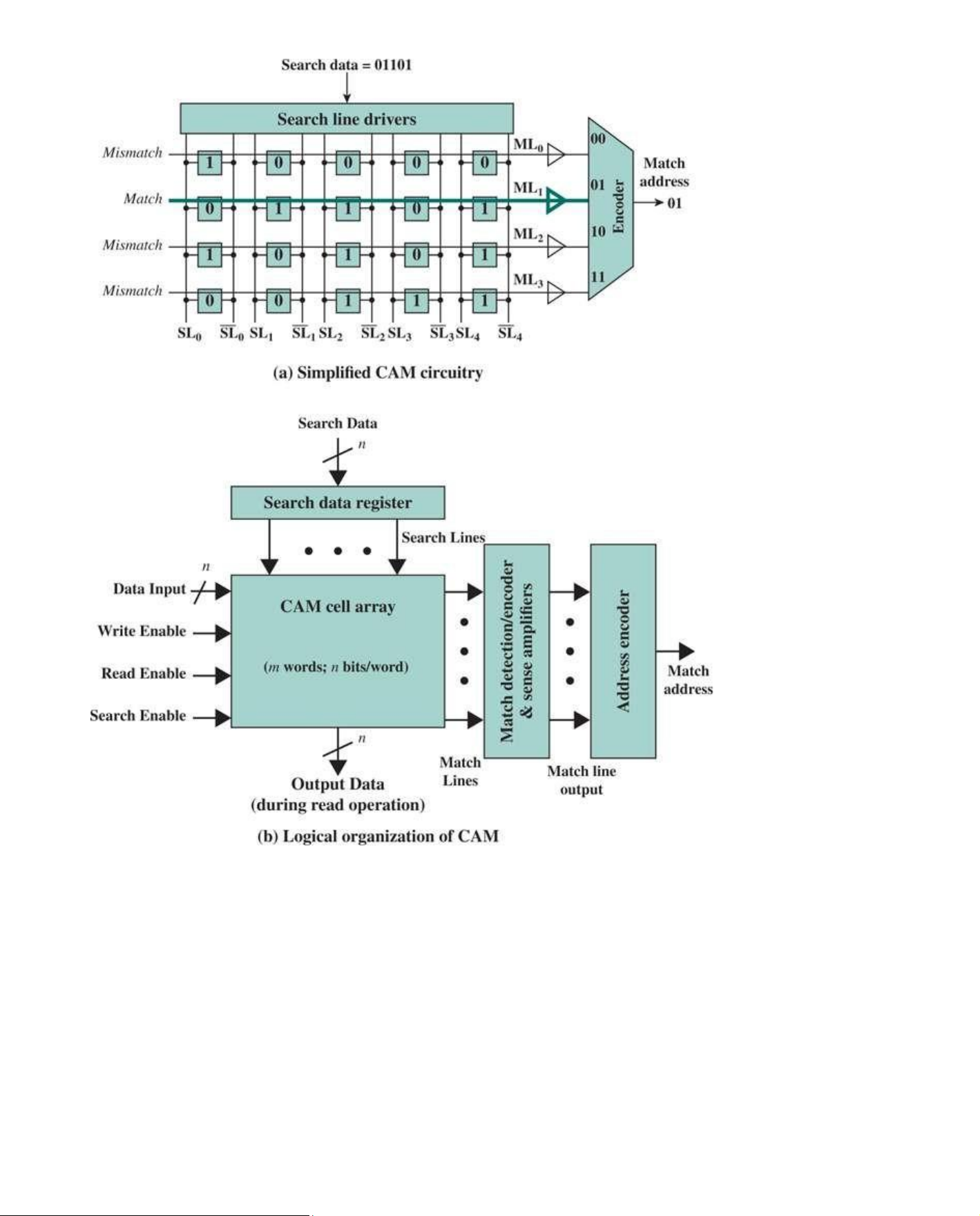
CONTENT-ADDRESSABLE MEMORY
Before discussing associative cache organization, we need to introduce the concept of
contentaddressable memory (CAM), also known as associative storage [PAGI06]. Content-
addressable memory (CAM) is constructed of static RAM (SRAM) cells (see static RAM) but is
considerably more expensive and holds much less data than regular SRAM chips. Put another way,
a CAM with the same data capacity as a regular SRAM is about 60% larger [SHAR03].
A CAM is designed such that when a bit string is supplied, the CAM searches its entire memory in
parallel for a match. If the content is found, the CAM returns the address where the match is found
and, in some architectures, also returns the associated data word. This process takes only one clock cycle.
Figure 5.9a is a simplified illustration of the search function of a small CAM with four horizontal
words, each word containing five bits, or cells. CAM cells contain both storage and comparison
circuitry. The is a match line corresponding to each word, feeding into match line sense amplifiers,
and there is a differential search line pair corresponding to each bit of the search word. The encoder
maps the match line of the matching location to its encoded address. lOMoAR cPSD| 58605085
Figure 5.9 Content-Addressable Memory
Figure 5.9b shows a logical block diagram of a CAM cell array, consisting of m words of n bits each.
Search, read, and write enable pins are used to enable one of the three operating modes of the
CAM. For a search operation, the data to be searched is loaded in an n-bit search register that
sets/resets the logic states of the search lines. The logic within and between cells of a row is such
that a match lines is asserted if and only if all the cells in a row match the search line values. A
simple read operation, as opposed to a search, is performed to read the data stored in the storage
nodes of CAM cells using Read Enable control signal. The data words to be stored in CAM cell
array are provided during a write operation through data input port. lOMoAR cPSD| 58605085 ASSOCIATIVE MAPPING
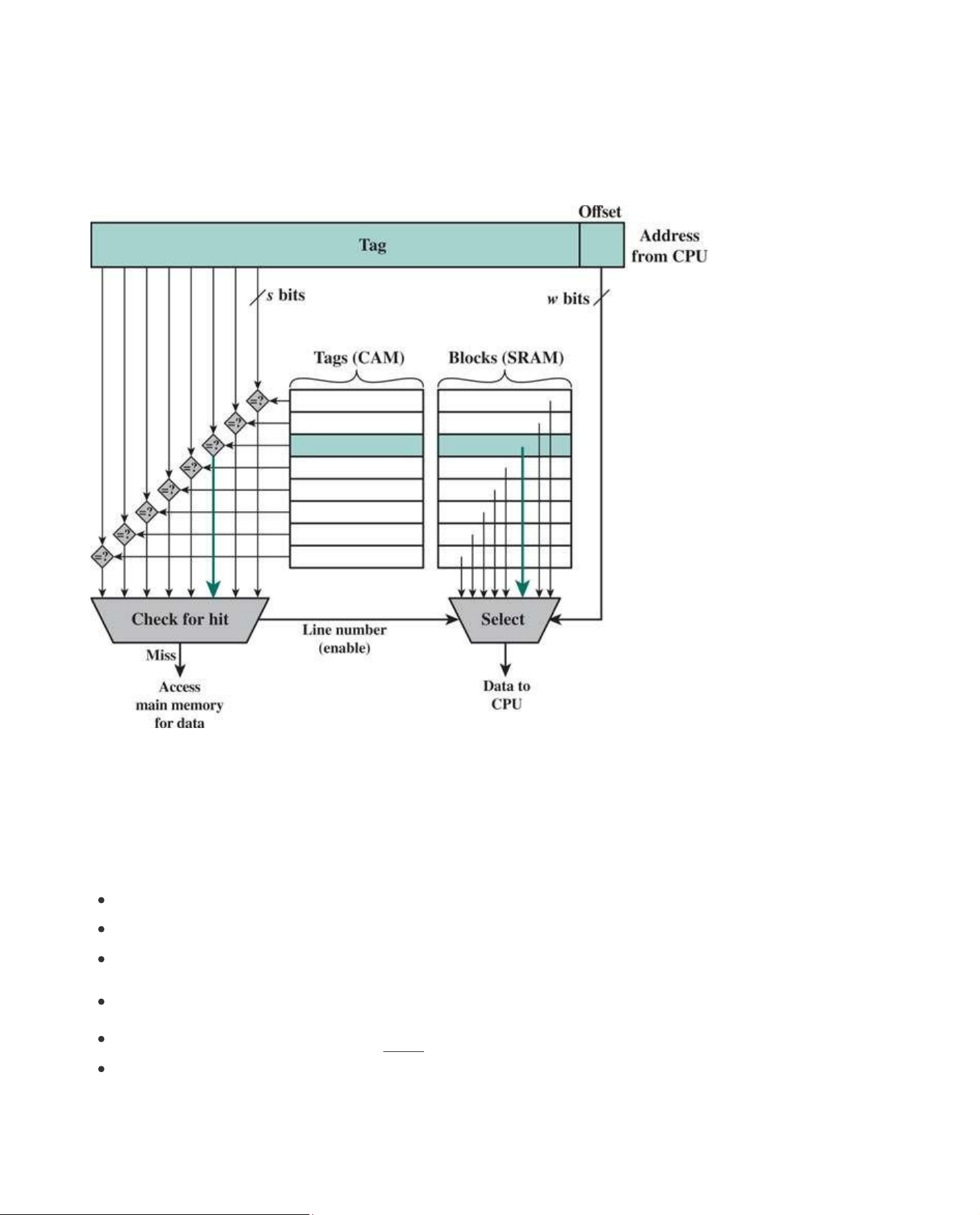
Associative mapping overcomes the disadvantage of direct mapping by permitting each main memory
block to be loaded into any line of the cache (Figure 5.6b). In this case, the cache control logic
interprets a memory address simply as a Tag and a Word field. The Tag field uniquely identifies a
block of main memory. To determine whether a block is in the cache, the cache control logic must
simultaneously examine every line’s tag for a match. Figure 5.10 illustrates the logic.
Figure 5.10 Fully Associative Cache Organization
Note that no field in the address corresponds to the line number, so that the number of lines in the
cache is not determined by the address format. Instead, if there is a hit, the line number of the hit is
sent to the select function by the cache hardware, as shown in Figure 5.9. To summarize,
Address length = (s + w ) bits s + w
Number of addressable units = 2 words or bytes w
Block size = line size = 2 words or bytes s + w 2 s
Number of blocks in main memory = w = 2 2
Number of lines in cache = undetermined lOMoAR cPSD| 58605085
Size of tag = sbits Example 5.1b
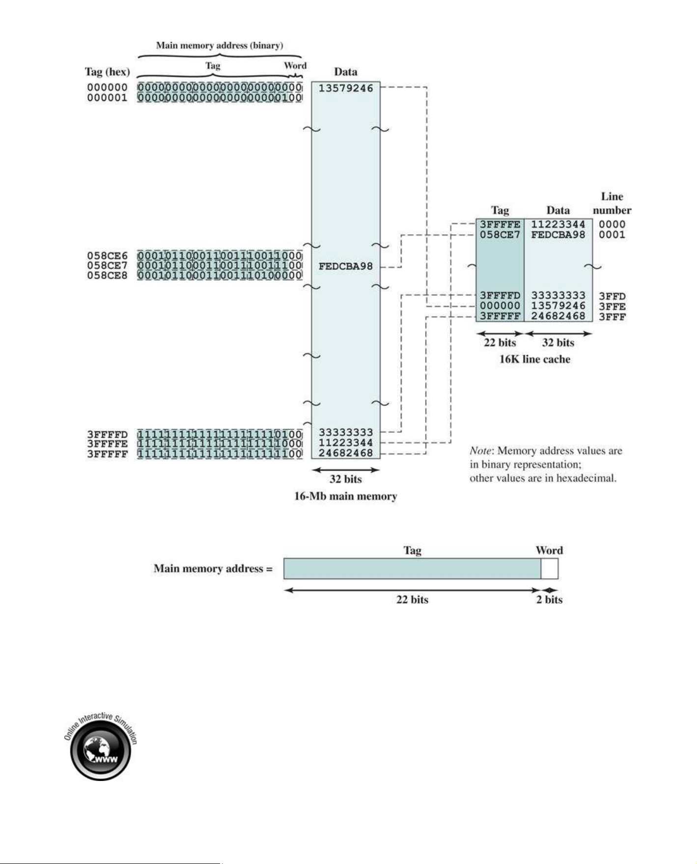
Figure 5.11 shows our example using associative mapping. A main memory address consists of a
22-bit tag and a 2-bit byte number. The 22-bit tag must be stored with the 32-bit block of data for
each line in the cache. Note that it is the leftmost (most significant) 22 bits of the address that form
the tag. Thus, the 24-bit hexadecimal address 16339C has the 22-bit tag 058CE7. This is easily seen in binary notation: Memory address 0001 0110 0011 0011 1001 1100 (binary) 1 6 3 3 9 C (hex) Tag (leftmost 22 bits) 00 0101 1000 1100 1110 0111 (binary) 0 5 8 C E 7 (hex) lOMoAR cPSD| 58605085
Figure 5.11 Associative Mapping Example
With associative mapping, there is flexibility as to which block to replace when a new block is read
into the cache. Replacement algorithms, discussed later in this section, are designed to maximize
the hit ratio. The principal disadvantage of associative mapping is the complex circuitry required to
examine the tags of all cache lines in parallel. Aleksandr Lukin/123RF lOMoAR cPSD| 58605085
Cache Time Analysis Simulator
SET-ASSOCIATIVE MAPPING
Set-associative mapping is a compromise that exhibits the strengths of both the direct and
associative approaches while reducing their disadvantages.
In this case, the cache consists of number sets, each of which consists of a number of lines. The relationships are m = v × k
i = j modulo v where i = cache set number j
= main memory block number m = number of lines in the cache v = number of sets k
= number of lines in each set This is referred to as k-way set-associative mapping. With set-
associative mapping, block B can be j mapped
into any of the lines of set j. Figure 5.12a illustrates this mapping for the first v blocks of main memory.
As with associative mapping, each word maps into multiple cache lines. For set-associative mapping,
each word maps into all the cache lines in a specific set, so that main memory block B0 maps into set
0, and so on. Thus, the set-associative cache can be physically implemented as v associative caches,
typically implemented as v CAM memories. It is also possible to implement the set-associative cache
as k direct mapping caches, as shown in Figure 5.12b. Each direct-mapped cache is referred to as a
way, consisting of v lines. The first v lines of main memory are direct mapped into the v lines of each
way; the next group of v lines of main memory are similarly mapped, and so on. The direct-mapped
implementation is typically used for small degrees of associativity (small values of k) while the
associative-mapped implementation is typically used for higher degrees of associativity [JACO08].
Tài liệu liên quan:
-

Revise C++: Create Your First OOP Project Guide | Môn Computer Architecture and Organization Lab - Đại học Sư phạm Kỹ thuật Thành phố Hồ Chí Minh
99 50 -

Bài 1 - Lập trình điều khiển đèn giao thông và RTC | Môn Computer Architecture and Organization Lab - Đại học Sư phạm Kỹ thuật Thành phố Hồ Chí Minh
149 75 -

Final Report Môn Computer Architecture and Organization Lab | Đại học Sư phạm Kỹ thuật Thành phố Hồ Chí Minh
126 63 -

Summary of HDL Coding Techniques & Considerations | Môn Computer Architecture and Organization Lab - Đại học Sư phạm Kỹ thuật Thành phố Hồ Chí Minh
134 67 -

Giới thiệu về Dữ liệu, Thông tin và Cơ sở dữ liệu | Môn Computer Architecture and Organization Lab - Đại học Sư phạm Kỹ thuật Thành phố Hồ Chí Minh
99 50