Design and Analysis of Current Mirror Circuits on HSPICE 180nm Technology
Design and Analysis of Current Mirror Circuits on HSPICE 180nm Technology. Tài liệu được sưu tầm giúp bạn tham khảo, ôn tập và đạt kết quả cao. Mời bạn đọc đón xem.
Môn: Tài liệu Tổng hợp 3.6 K tài liệu
Trường: Tài liệu khác 3.9 K tài liệu
Tác giả:
Preview text:
International Journal on Recent and Innovation Trends in Computing and Communication ISSN: 2321-8169 Volume: 5 Issue: 6 1191 – 1195
_______________________________________________________________________________________________
Design and Analysis of Current Mirror Circuits on HSPICE 180nm Technology S. Archana, Dr. B. K. Madhavi, Dr. I V Murlikrishna ECE dept. BRECW ECE dept, SWEC, Gandipet JNT University, Hyderabad, India Hyderabad, India Hyderabad , India
archanasubhash2006@yahoo.co.in
bkmadhavi2009@gmail.com iyyanki@gmail.com
Abstract— Current mirrors are one of the most common buildings blocks both in analog and mixed-signal VLSI circuits. Current
mirrors are very useful elements for performing current mode analog signal processing. It generated dc current in direct ratio with
reference current.Thus used for biasing integratred circuits also as active load in amplifier design, scaling and replication purpose.
This paper presents design and analysis of basic NMOS and PMOS current mirror with various conditions and also few concepts
likecurrent steering and scaling, source degenerative circuit to improve output impedance.Synopsys HSPICE circuit simulator
with Stanford NMOS and PMOS model at 180nm technology atVDD of 1.8V is used for simulation of all circuit. Simulation
result shows NMOS current mirror power consumption of 3.9μW while PMOS current mirror takes 25μW
power. Source degenerative circuit shows output impedance of 1203MΩ.
Keywords-VLSI,HSPICE,CM
__________________________________________________*****_________________________________________________ I. I NTRODUCTION µ �
Transistors are frequently used active device in analog ICs. � = − 2 2 �
For operation of ICs, proper biasing is essential. A current 1 (1)
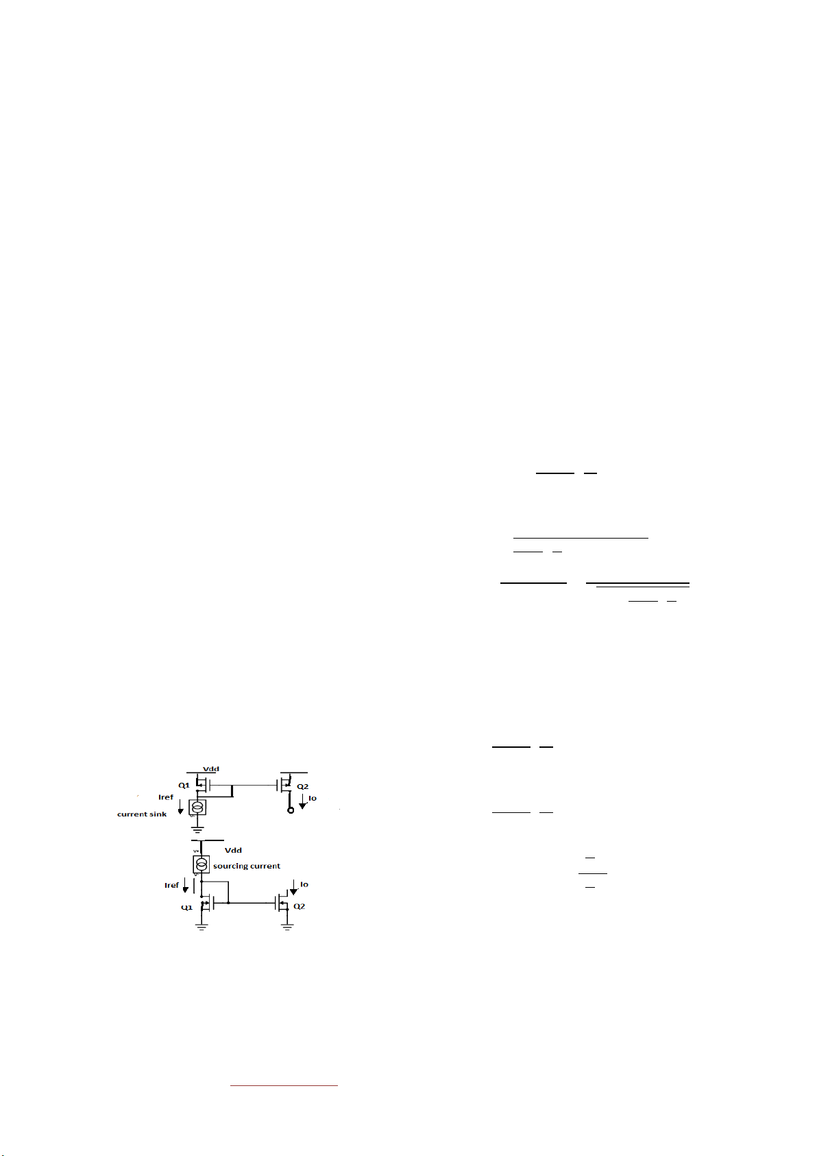
mirror is an element with at least three terminalswhich can be where
used as source or sink as shown in figure 1. The common −
terminal is connected to a power supply or ground,The output � = µ �
current is equal to the input current multiplied by a desired − 2 2 � 1
current gain[1]. If the gain is unity, the input current is − 1
reflected to the output, leading to the name current mirror. = � − µ �
Current mirrors are very useful elements for performing � ( 2 �
current mode analog signal processing.They are used in design 1
of neural network based current mode winner take all circuit to
If different W/L ratio transistors are used, current
determine min or max among n input signals.Therefore their
mirrors can be used as current multiplier as
designs must fulfill the following requirements [2]: shownbelow.
1. Input impedance should be zero
2. Output impedance should be infinite From the figure 1
3.Output current should be constant over wide swing of voltage µ �
4. Accurate copy of input current. − 2 = � 2 � 1 µ � − 2 = � 2 � 2 � � = 2 . � � 1 (2) II.
SIMPLE NMOS CURRENT MIRROR
Figure 1NMOS andPMOS current source and sink
Current mirror acts as a resistor and its internal resistance is
Neglecting channel length modulation,
internal resistance of transistor M2. M1 is used to provide
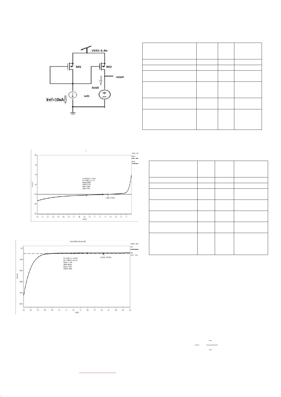
biasing[3].Figure2 is designed for reference current of 460μA. 1191
IJRITCC | June 2017, Available @ http://www.ijritcc.org
_______________________________________________________________________________________
International Journal on Recent and Innovation Trends in Computing and Communication ISSN: 2321-8169 Volume: 5 Issue: 6 1191 – 1195
_______________________________________________________________________________________________
III. NMOS CASCODE CURRENT MIRROR WITH VSS AND IREF=10 ΜA
In our simulation we look at a 1/0.5 current mirror for
10 μ A where we load the mirror output with a voltage source.
This voltage is dc sweeped and we look at the output current.
We can get the perfect mirror output current, when we have
VDS = VGS[3]. To achieve this we use a cascode to set VDS
of the output transistor M3 to its VGS as shown in figure 5.
Gate of transistor is biased properly which keeps the transistor
in linear region. For this we need a cascode VGS voltage of
twice the threshold voltage for the input current[4]. As we can
see in the plot the current is more stable. This is because VDS
of M3 is now fixed to a value where the early effect cancelled
as a diode connected NMOS transistor has VGS = VDS so we
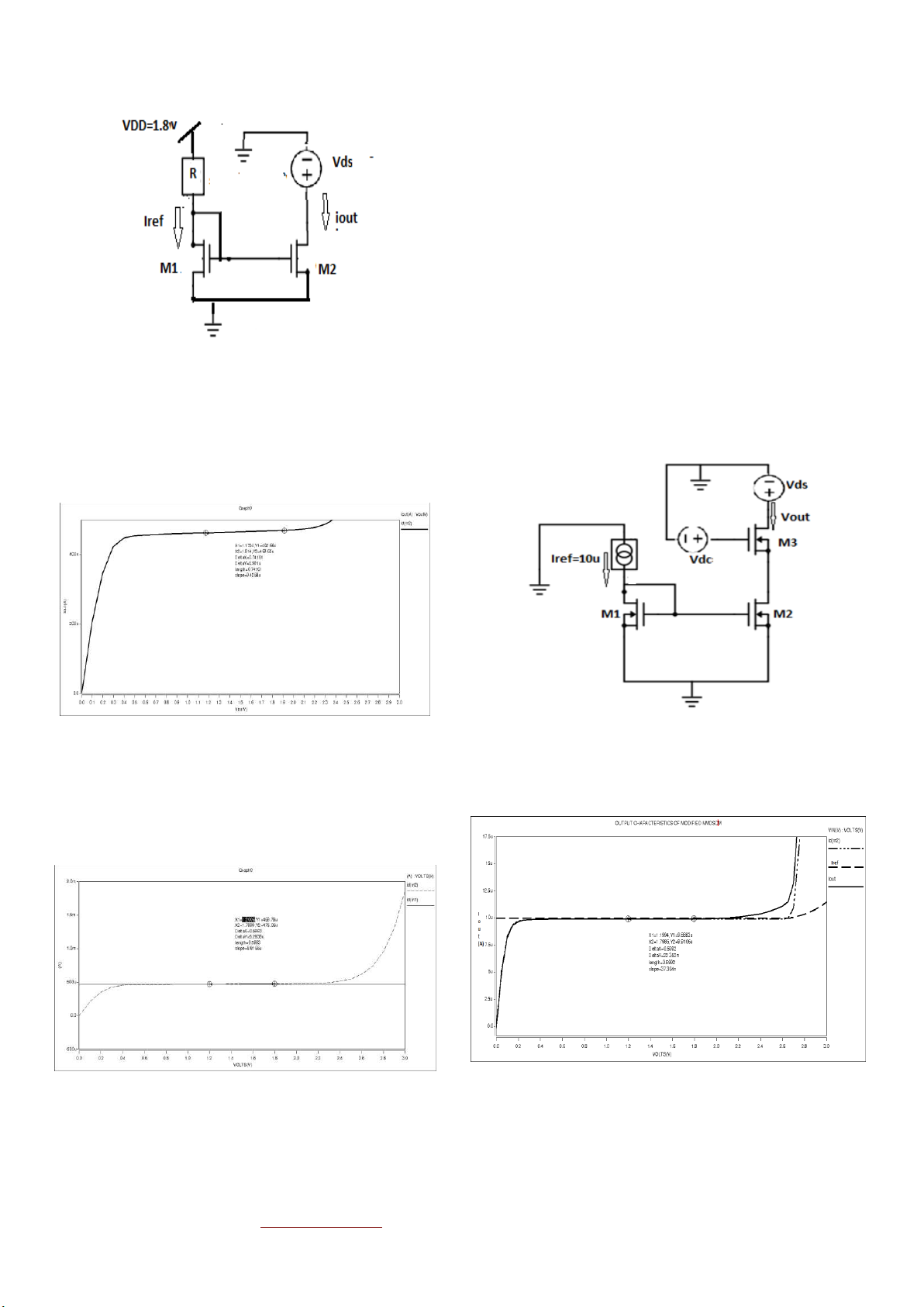
Figure 2 NMOS current mirror without VSS for Iref=460 μA
see that the curve has a quadratic part and a linear part which
As shown in figure 2, reference current is copied in output
is defined by the early voltage i.e. 1/vearly = lambda[5].
transistor M2 after proper biasing. Based in the given data of
Power dissipation is reduced as compared to basic NMOS
reference current of 460μA, R= 2K,select appropriate value of
current mirror but gain is slightly reduced as shown in table 1.
W/L ratio for both transistors such that Iout will be same as that
Iref by using standard current equation(2) DC analysis was
done. Figure3 shows the response for output characteristics.
Figure 5 Cascode NMOS CM for Iref=10μA
Figure 3 Output characteristics of basic NMOS CM
DC Analysis shows output is stable for more duration
Analysis shows output current is almost equal to input current.
compared to basic NMOS current mirror. Figure 6 shows
Various parameters calculated are listed in table 1.Same circuit output characteristics.
was simulated by applying VSS of -1.8V to improve output
voltage swing at the cost of high power dissipation.. The DC
simulated result is as shown in figure 4.
Figure 6 Output characteristics of cascode NMOS CM
Figure 4 Output characteristics of basic NMOS CM with VSS 1192
IJRITCC | June 2017, Available @ http://www.ijritcc.org
_______________________________________________________________________________________
International Journal on Recent and Innovation Trends in Computing and Communication ISSN: 2321-8169 Volume: 5 Issue: 6 1191 – 1195
_______________________________________________________________________________________________
IV. SIMPLE PMOS CURRENT MIRROR
Table 1 Comparison of various basic NMOS CM NMOS Current Mirror Iref(A) Gain Power dissipation (W) without VSS with R 460μ 1 1.24m with VSS,R 460μ 1 4.57m With current source and 460u 0.99 679 μ 2 NMOS Modified with current 460u 0.95 512 μ source and 3 NMOS(cascode) With current source and 10μ 1 3.9μ 2 NMOS Modified with current 10μ 0.89 1.186μ source and 3 NMOS to
Figure 7 Basic PMOS current mirror reduce power dissipation
Figure 7 shows schematic diagram for basic PMOS
current mirror.DC analysis without VSS and with
VSSshows output characteristics as shown in figure 8
Table 2 shows comparison between various PMOS current and 9. mirror analyzed in our work.
Table 2 Comparison of various basic PMOS CM PMOSCurrent Iref Gain Power Mirror (A) dissipation (W) without VSS with R 460μ 1 1.47m with VSS,R 460μ 1 3.9m With current source 460u 1 1.42m and 2 PMOS With VSS,current 460u 1 169m source and 2 PMOS Modified with current 460u 1 1.485m source and 3 PMOS With current source 10μ 1 25μ
. Figure 8 Output characteristics of basic PMOS CM and 2 PMOS 10μ Modified with current 1 28.5μ source and3 PMOS to reducepower dissipation V. CURRENT STEERING CIRCUIT
Current steering plays an important role in design of
determining highest or lowest signal strength input signal [6].
This concept is used in winner take all circuit used as MAX or
MIN circuit in pattern recognition applications.Drain current
of M3 comes from drain of M4[7]. Hence I4=I3 can steer a
current from NMOS current mirror to PMOS current mirror or
vice versa as shown in figure 10. NMOS transistor should
Figure 9 Output characteristics of basic PMOS CM with VSS
match mutually also PMOS transistor should match such that
Table 1 shows comparison for various NMOS current mirrors Vth4=Vth5[11,12]. analyzed. �5 5 � � = = 1 4 4 � 1193
IJRITCC | June 2017, Available @ http://www.ijritcc.org
_______________________________________________________________________________________
International Journal on Recent and Innovation Trends in Computing and Communication ISSN: 2321-8169 Volume: 5 Issue: 6 1191 – 1195
_______________________________________________________________________________________________ (3)
Thus source current I5 can be related to reference current Iref as . �5 3 5 � � � = . 1 4 � � (4)
Figure 12 Schematicof Currentmirror for scaling purpose
. The change is due to channel length modulation factor[8].
Table 3 shows DC characteristics for the same. Figure 11 showsoutput characteristics.
Figure 13Output characteristics of Current mirror for scaling purpose
Figure 10Current steering circuit
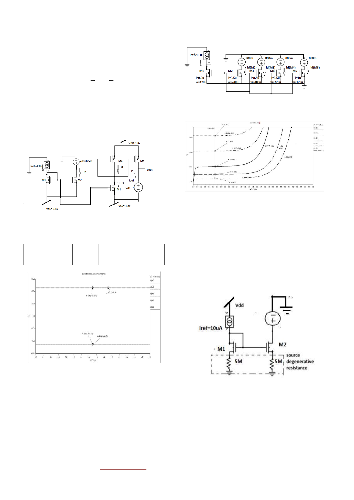
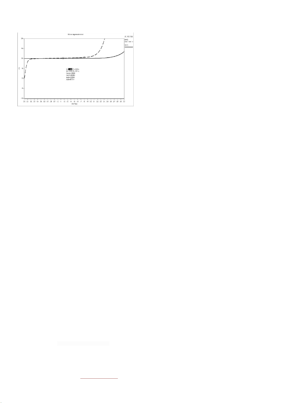
VII SOURCE DEGENERATION CURRENT MIRROR
TABLE 3 DC CHARACTERISTICS OF CURRENT
Schematic diagram for source degeneration current mirror is as STEERING CIRCUIT
shown in figure 14.It is used to improve output
impedance[10,13]. Table 4 compares output impedance without Iref(A) Rin(Ω) R0(Ω) Gain Power R and with R dissipation(W) 460μ 530 178K 0.98 2.4750m
(source degeneration circuit).It is found that rout is improved
by a factor 500. Figure 15 shows output characteristics of
source degenerative resistance circuit.
Figure 11 Output characteristics of current steering circuit
VI. CURRENT MIRROR FOR SCALING PURPOSE
Figure 14Source degeneration circuit
Depending on aspect ratio output current can be made integral
Without source degeneration output impedance was 2MΩ
multiple of reference current[9]. Figure 12 shows its use in
while with source degeneration circuit it is improved and is
scaling. Transistor M2 has twice width of transistor M1 hence equal to 1203MΩ .
Id(M2) is doubled while for M5 width is halved hence
Id(M5)also halved. Figure 13shows output response. Voltage
source power dissipation was 104.8854μwatts. 1194
IJRITCC | June 2017, Available @ http://www.ijritcc.org
_______________________________________________________________________________________
International Journal on Recent and Innovation Trends in Computing and Communication ISSN: 2321-8169 Volume: 5 Issue: 6 1191 – 1195
_______________________________________________________________________________________________
[10] BjörnEversmann, Martin Jenkner, Franz Hofmann, Roland,”A 128
128 CMOS Biosensor Array for Extracellular Recording of Neural
Activity” IEEE Journal of solid state circuits Vol. 38, No(12) on 12
December 2003 IEEE tranactions on circuits and systems II
Express Vol(51) issue(3), March 2004, pp 124-129
[11] BeniaminDragoi.,“IEEE improved first generation current
conveyor based on self cascode current mirror”,18th
Telecommunications forum Telforserbia, Belgrade,Nov 23- 25,2010.
[12] Khalil Monfaredi, Hassan FArajiBAghtash,MAsidAbbasi,” A
novel low power vert low voltage high performance current
mirror” International scholarly and scientific research and Innovation International Journal of Electrical
Computers,Energetic,Electronic and Communication Engineering Vol 4 No(4),2010,pp1454-1458.
[13] Hassan FarajiBaghtash,S A Azari ,”Very low impedance low
Figure 9 Output characteristics of source degeneration circuitt
power current mirror”, Analog Integrated IC and signal processing .Vol66 issue (1),2011pp 9-18. CONCLUSION
Simulation on various designs of basic NMOS
current mirror using HSPICE 180n technology at VDD of
1.8V shows input impedance is least in simple NMOS current
mirror. Power dissipation of PMOS current mirror is more
than NMOS current mirror. Power dissipation is least in
modified cascode arrangement.For low power design it is
useful. Apart from this various concepts useful in analog VLSI
signal processing like use of current steering circuit, current
scaler circuit, source degeneration circuit are analyzed. ACKNOWLEDGMENT I would like to thank my guide Dr. B.K
Madhavimadam,whose constant support inspired me to work
on this topic. I also thank my guide Dr. I V Murali Krishna for
his valuable suggestions and guidance. REFERENCES
[1] C A Mead ,” Analog VLSI and neural systems”, Addison Wesley, 1989
[2] E. Sackinger, W. Guggenbuhl ,” A high-swing, high impedance
MOS cascode circuit”, IEEE J. Solid State Circuits, Vol 25 No(1),1990, pp 289-298
[3] S S Rajput S S .Jamur “,A high performance current mirror for
low voltage designs”,Asia pacific conference on circuits and systems,Dec 2000, pp 170-173
[4] S S Rajput S SJamur ,” Low voltage Low power high
performance current mirror for portable analogue and mixed mode
applications”, IEEE proceedings circuits devices and systems Vol
148 No(5) Oct 2001, pp 273-278
[5] K H Cheung, Chi Che chain, Chun fu Chung “Accurate current
mirror with high output impedance”, IEEE Electronics circuitsand a. systems Conference 0-7803-7057-0, , 2.5 September,2002, pp 565-568.
[6] RazaviBehzad,”Design of Analog CMOS Integrated circuits”, 2002
[7] Rajput, S. S., Low voltage current mode circuit structures and their
applications Thesis, Indian Institute of Technology, Delhi,2002.
[8] S S Rajput Jamur,”A Current Mirror for Low Voltage, High
Performance Analog Circuits Analog IC and signal
processing”,Vol36,No(3)Sept ,2003,pp 221–233
[9] K.-H. Cheng, T.-S. Chen and C.-W. Kuo ,”“High Accuracy
Current Mirror with Low Settling Time”,Proceedings of the 46th
IEEE International Midwest Symposium on Circuits and Systems ,2003pp 1189-1192. 1195
IJRITCC | June 2017, Available @ http://www.ijritcc.org
_______________________________________________________________________________________
Tài liệu liên quan:
-

Ung dung game hoa trong cac chien dich MKT
18 9 -

Bao cao Chi so TMDT Viet Nam 2025
15 8 -

Thông tư quy định về việc phân quyền, phân cấp và phân định thẩm quyền quản lý nhà nước về giáo dục cho chính quyền địa phương
24 12 -
Nghị quyết về phát huy các giá trị di sản văn hóa gắn với phát triên du lịch bền vững tỉnh Khánh Hòa đến năm 2025, định hướng đến năm 2030
14 7 -

Quyết định phê duyệt Chiến lược phát triển du lịch Việt Nam đến năm 2030
13 7