Design of a Low Cost Short Range Underwater Acoustic Modem | Đại học Bách Khoa, Đại học Đà Nẵng
Design of a Low Cost Short Range Underwater Acoustic Modem | Đại học Bách Khoa, Đại học Đà Nẵng giúp sinh viên tham khảo, ôn luyện và phục vụ nhu cầu học tập của mình cụ thể là có định hướng, ôn tập, nắm vững kiến thức môn học và làm bài tốt trong những bài kiểm tra, bài tiểu luận, bài tập kết thúc học phần, từ đó học tập tốt và có kết quả cao cũng như có thể vận dụng tốt những kiến thức mình đã học
Môn: Công nghệ web 18 tài liệu
Trường: Trường Đại học Bách khoa, Đại học Đà Nẵng 1.7 K tài liệu
Tác giả:

Preview text:
Design of a Low-Cost, Underwater Acoustic Modem
for Short-Range Sensor Networks B. Benson, Y. Li, R. Kastner
B.Faunce, K. Domond, D. Kimball, C. Schurgers
Department of Computer Science and Engineering
California Institute for Telecommunications and
University of California San Diego Information Technology, UCSD La Jolla, CA 92093 La Jolla, CA 92093
Abstract- A fundamental impediment to the use of dense
long-range, expensive systems rather than small, dense, and
underwater sensor networks is an inexpensive acoustic modem.
cheap sensor-nets [6]. It is widely recognized that an open-
Commercial underwater modems that do exist were designed for
architecture, low cost underwater acoustic modem is needed to
sparse, long range, applications rather than for small, dense,
truly enable advanced underwater ecological analyses.
sensor nets. Thus, we are building an underwater acoustic
modem starting with the most critical component from a cost
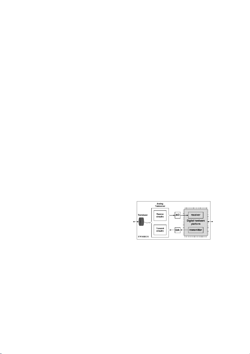
Underwater acoustic modems consist of three main
perspective – the transducer. The design substitutes a
components (Figure 1): (1) an underwater transducer, (2) an
commercial transducer with a homemade transducer using cheap
analog transceiver (matching pre-amp and amplifier), and (3)
piezo-ceramic material and builds the rest of the modem’s
a digital platform for control and signal processing. A
components around the properties of the transducer to extract as
substantial portion of the cost of the modem is the underwater
much performance as possible. This paper presents the design transducer; commercially available underwater omni-
considerations, implementation details, and initial experimental
directional transducers (such as those as seen in existing results of our modem.
research modem designs [7-9]) cost on the order of $2K-$3K. I. INTRODUCTION
Commercial transducers are expensive, due to the cost of
Our fundamental knowledge of aquatic ecosystems is
ensuring consistent quality control of manufacturing
increasing at a tremendous rate due to the physical, chemical
piezoelectric materials and potting compounds, expensive
and biological time-series data from long term sensors. As a
calibration equipment and time-consuming characterization,
result, research sites around the world are being equipped with
all further exacerbated by low volume production. Therefore,
a broad range of sensors and instruments. Despite the
much of the design for the low-cost modem lies in finding an
substantial effort to monitor ecological aspects of aquatic
appropriate substitute for the custom commercial transducer.
systems, the infrastructure needed for sensor networks in
Jurdak et al. substituted the transducer with generic,
marine and freshwater systems without question lags far
inexpensive, speakers and microphones, but were only able to
behind that available for terrestrial counterparts.
obtain a data rate of 42 bps for a transmission range of 17m
There is increasing interest in the design and deployment of
[10]. Benson et. al substituted a custom transducer with a
underwater acoustic communication networks. For example,
commercially available fish finder transducer (which cost $50),
the Persistent Littoral Undersea Surveillance Network
but was only able to obtain a data rate of 80 bps for a
(PLUSNet) demonstrates multi-sensor and multi-vehicle anti-
transmission range of 6m [11]. Furthermore, these fish finders
submarine warfare (ASW) by means of an underwater
have a < 5 degree beam width, making them less than ideal for
acoustic communications network [1]. A short range shallow most deployment scenarios.
water network to monitor pollution indicators in Newport Bay,
CA is proposed in [2]. A network of acoustic modems akin to
motes is proposed for low power, short range acoustic
communications for seismic monitoring [3]. A swarm of
acoustically networked autonomous drifters is envisioned to
monitor phenomena as they are subjected to ocean currents [4].
A 1km x 1km underwater wireless network of 10s of
temperature sensors is envisioned to obtain high temporal and
spatial resolution observations within the coral reef lagoon at
the Moorea Coral Reef Long Term Ecological Research Station [5].
Figure 1. Major components of an underwater acoustic modem
In order to make more short-range underwater acoustic
communication networks a reality, the cost of underwater
In this paper, we present the design of a short-range
acoustic modems must come down. Commercial off-the-shelf
underwater acoustic modem starting with the most critical
(COTS) underwater acoustic modems are not suitable for
component from a cost perspective – the transducer. The
short-range (~ 100m) underwater sensor-nets: their power
design substitutes a commercial underwater transducer with a
draws, ranges, and price points are all designed for sparse,
homemade underwater transducer using cheap piezoceramic
978-1-4244-5222-4/10/$26.00 ©2010 IEEE
material and builds the rest of the modem’s components
ensure the leads would not pick up unwanted electromagnetic
around the properties of the transducer to extract as much
noise and attached the leads using solder with 3% silver.
performance as possible. We describe the design
The piezoelectric ceramic needs to be encapsulated in a considerations, implementation details, and initial
potting compound to prevent contact with any conductive
experimental results of our modem prototype.
fluids. Urethanes are the most common material used for
The remainder of this paper is organized as follows.
potting because of their versatility. The most important design
Section II describes the design of our homemade transducer
consideration is to find a urethane that is acoustically
and its experimentally determined electrical and mechanical
transparent in the medium that the transducer will be used; this
is more important for higher frequency or more sensitive
properties. Section III describes the design of our analog
applications where the wavelength and amplitude is smaller
transceiver and Section IV describes the design transceiver.
than the thickness of the potting material. Generally, similar
We present experimental results in Section V and compare the
density provides similar acoustical properties. Mineral oil is
power and cost of our modem to existing modem designs in
another good way to pot the ceramics because it is inert and
Section VI. We conclude with a discussion on future work in
has similar acoustical properties as water. Some prefer using Section VII.
mineral oil to urethane because it is not permanent. However, II. TRANSDUCER
the oil still needs to be contained by something, which is often
a urethane tube. We selected a two-part urethane potting
In this section we describe the design of our homemade
compound, EN12, manufactured by Cytec Industries [13] as it
transducer, explaining the reasons behind the selection of its
has a density identical to that of water, providing for efficient
piezo-ceramic, urethane compound, and wire leads. We then
mechanical to acoustical energy coupling.
present the transducer’s experimentally determined electrical
Creating a transducer by potting the ceramic shifts its
and mechanical properties which are used to govern the rest of
resonance frequency due to the additional mass moving the modem design.
immediately around the transducer. The extent of the shift A. Transducer Design depends on the potting compound’s characteristics. Underwater transducers are typically made from
Characteristics can vary depending on the type, age,
piezoelectric materials – materials (notably crystals such as
temperature, and mixing method of the compound. The
lead zirconate titanate and certain ceramics) that generate an
amount of potting can influence resonance frequency as well.
electric potential in response to applied mechanic stress and
Having tight control over these variables to ensure exact
produce a stress or strain when an electric field is applied. For
reproducibility requires expensive equipment. To keep costs
underwater communication, transducers are usually omni-
low, we used a simplistic potting method, pouring and mixing
directional in the horizontal plane to reduce reflection off the
the compound by hand in a thermostat controlled lab.
surface and bottom. This is especially important for shallow
Experimental results described in the next subsection indicate water communications.
that the transducer variations caused in our simplistic potting
The 2D omni-directional beam pattern can be achieved
procedure are suitable for our intended application.
using a radially expanding ring or using a ring made of several
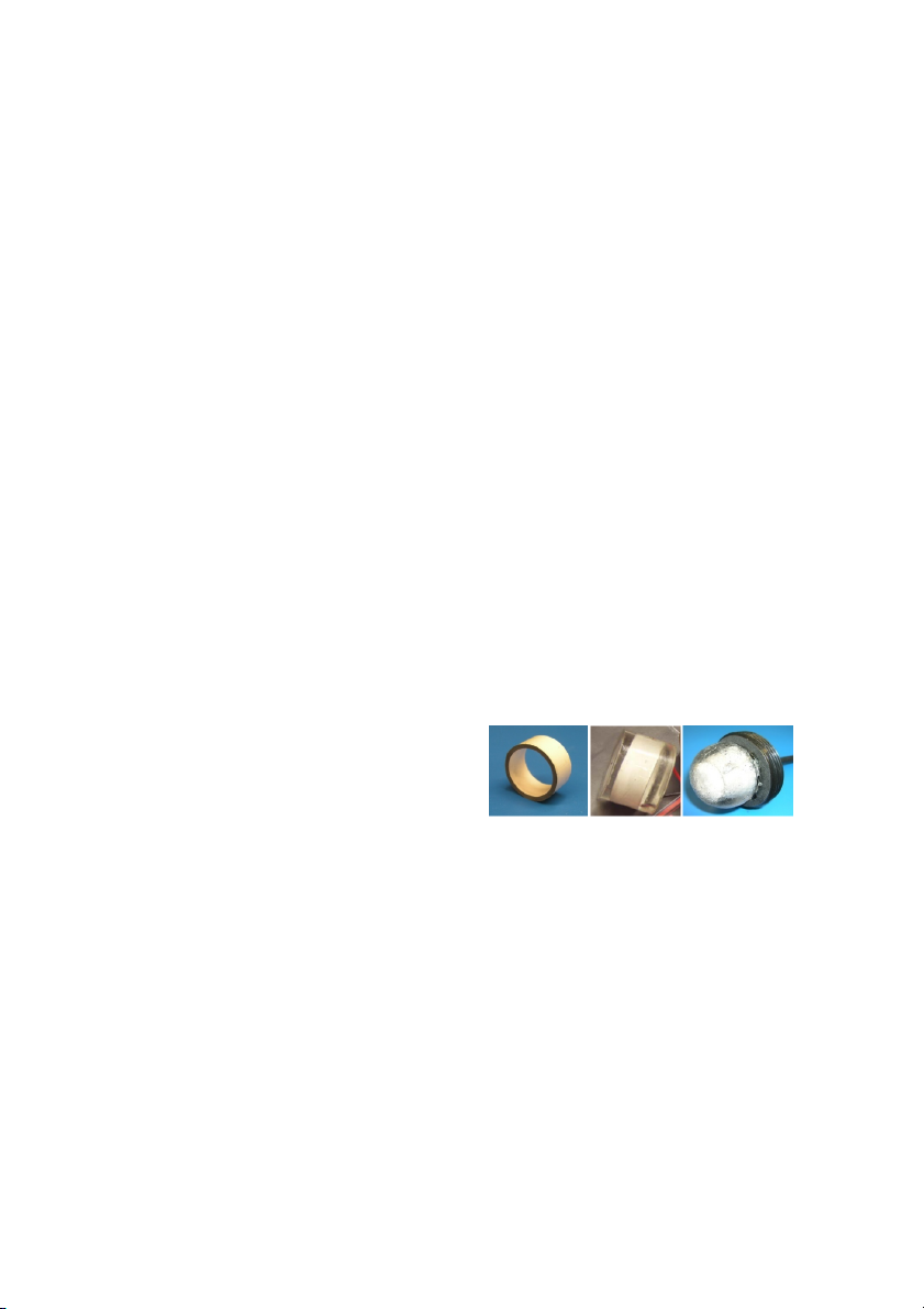
Figure 2 shows the piezo-ceramic ring, the potted ceramic,
ceramics cemented together. A radially expanding ceramic
and the transducer in the potting compound mounted to a
ring provides 2D omni-directionality in the plane
prototype plate to be attached to the modem housing. The total
perpendicular to the axis and near omni-directionality in
cost of our transducer, including the ceramic, leads, potting
planes through the axis if the height of the ring is small
and labor is approximately $50.
compared to the wavelength of sound being sent through the
medium [12]. The radially expanding ceramic is relatively
inexpensive to manufacture. A ring made of several ceramics
cemented together provides greater electromechanical
coupling, power output, and electrical efficiency; the piezoelectric constant and coupling coefficient are
approximately double that of a one-piece ceramic ring [Ken1].
They work better because the polarization can be placed in the
Figure 2. From left to right: The raw piezoelectric ring ceramic, the potted
direction of primary stresses and strains along the
ceramic, the transducer in the potting compound mounted to a prototype plate
to be attached to a modem housing.
circumference. However, these are much more difficult to
manufacture and are therefore much more expensive than a
B. Transducer Properties
one piece radial expanding piezoelectric ceramic ring. We
For a single radially expanding ceramic ring, the resonance
thus selected to use a single radially expanding ring, a <$10
frequency occurs when the circumference approximately
Steminc model SMC26D22H13SMQA to achieve an omni-
equals the operating wavelength [12, 14]. In air, this frequency
directional beam pattern at low-cost.
is about 41 kHz for every inch in diameter of a solid radially
The most common method of making transducers from a
expanding ceramic ring; for the ring made of several ceramics
ring ceramic is to add two leads, and pot it for waterproofing
cemented together, in the case that there is not inactive
[12]. We used shielded cables for the transducer leads to
material (such as electrodes or cement), the resonance
frequency is approx 37 kHz for every inch [12]. The
The experimental procedure to d etermine the transducer’s
SMC26D22H13SMQA has an outer diameter of 1.024 inches,
TVR and RVR included placing our transducer in water 1
a wall thickness of 0.1 inches and a height of 0.512 inches.
meter apart from a reference transducer with a known TVR
Steminc specifies that the ceramic ring has a nominal
and RVR (in our case, an ITC1042 [16]) in the middle of a 3
resonance frequency of 43kHz +/- 1.5kHz. Experimentally
meter deep, 2 meter wide cylindric
c al test tank, and collecting
measuring the impedance of two different ceramics (Figure 3)
signals swept across frequencies, 31 k-90kHz in 1kHz
shows the ceramics do fall within this specification. The
increments, sent from the reference transducer to our
resonance frequency (~43kHz) and anti-resonance frequency
transducer and vice versa. We then calc ulated the RVR and
(~45kHz) occur at minimum and maximum impedances,
TVR of our transducer based on the collected data and the respectively [14, 15].
reference’s TVR and RVR. Figures 5 and 6 show the TVR and RVR of transducer T1. T1 TVR 144 142 m 140 1 @ 138 /V a P u 136 1 re B 134 d 132
Figure 3. The SMC26D22H13SMQA ceramic impedance (and
resonance frequency) in air of two ceramics (T1, T2) 13030 40 50 60 70 80 90
As stated in the previous subsection, potting the ceramic Frequency [kHz]
shifts the resonance frequency due to the additional mass
Figure 5. Experimentally determined transmitting voltage response for
moving immediately around the transducer. Figu re 4 shows transducer T 1
the extent of this shift and the relatively small variation T1 RVR
(caused by the ceramic’s variation and the po tting procedure) -190
between two different transducers (potted us ing the ceramics
T1 and T2 from Figure 3). Transmitt ing around the -195
transducer’s resonance frequency (35kHz) provides the most
efficient electrical to acoustical energy coupling [12,14]. a -200 P u /1 V -205 1 re B -210 d -215 -22030 40 50 60 70 80 90 Frequency [kHz]
Figure 6. Experimentally determined receiving voltage response for transducer T 1
Figure 4. The transducer impedance and resonance frequency (~35kHz) of
The max response of the TVR an d RVR do not necessarily
transducers potted from ceramics T1 and T2
occur at the transducer’s electrical resonance (as seen in
Figures 5 and 6), but the transducer’s resonance frequency still
To characterize the transducer’s electro-mechanical
falls near the peak. The sharp peak s and valleys of TVR and
p roperties, we experimentally measured its transmitting
RVR can be attributed to inefficiencies in the calibration
voltage response (TVR) and its receiving voltage response
procedure and characteristics of resonance that are directly
(RVR). The TVR is defined as the soun d pressure level
related to geometry of the PZT. To obtain a flatter, smoother
experienced at 1m range, generated by the transducer per 1 V
TVR and RVR (such as those for [16]), more expensive
of input Voltage and is a function of frequenc y. The RVR is a
ceramics and manufacturing and calibration procedures are
measure of the voltage generated by a plane wave of unit required.
acoustic pressure at the receiver and is a function of frequency.
In addition to the TVR and RVR, an important parameter of
per unit depending on the quantity produced. The transmitter
a transducer is how much voltage it can tolerate before it
and receiver portions of the analog transceiver are described in
breaks A typical Type I PZT’s can experience up to 12 volts
more detail in the following subsections.
AC per .001 inches wall thickness without much effect to its
electro-mechanical properties[17]. Thus, voltages up to
1200Vpp or 425Vrms should be used for our transducer.
Using the passive sonar equation we can calculate the
expected max distance the transducer will be able to send a
signal given a Source Level (SL), the transmission loss (TL,
due to spreading and absorption loss in the water), and the
noise level (NL) of the ocean. SNR = SL – TL - NL (1)
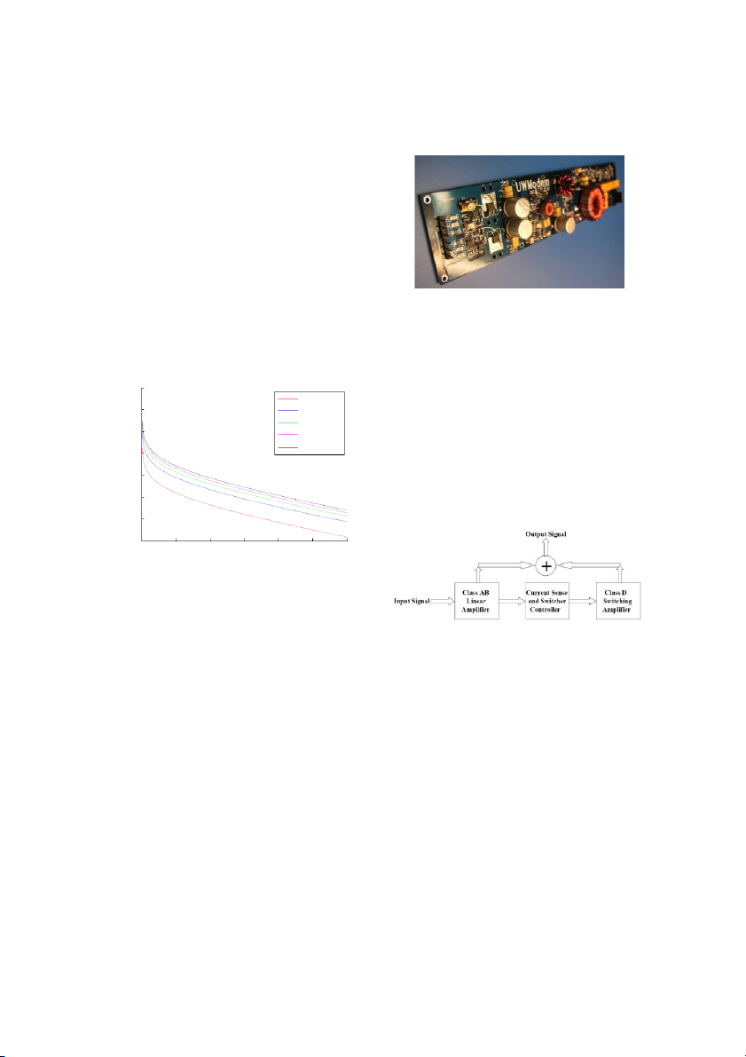
Figure 7 shows the expected max distance achievable for
the transducer transmitting at the transducer’s resonance Figure 8. Analog Transceiver
frequency at various voltages assuming a noise level of 50 dB
r 1 uPa.. Transmitting 425 Vrms, for an SNR of 10 dB re 1 C. Analog Transmitter
uPa at the receiver, the transducer could theoretically send a
The transmitter was designed to operate for signal inputs
signal up to 2800 meters. The receive voltage at 10 dB SNR
in a range of 0 – 100kHz. The architecture is unique
(determined using the RVR) is 820uV.
andconsists of two different amplifiers working in tandem
(Figure 9). The primary amplifier is a highly linear Class AB SNR vs. Range
amplifier that provides a voltage gain of 23 while achieving a 120
power efficiency of about 50%. The output of the Class AB 25 Vrms 100
amplifier is connected to current sense circuitry that in turn 125 Vrms
controls the secondary amplifier, which is a Class D switching 225 Vrms 80
amplifier. The Class D amplifier is inherently nonlinear but 325 Vrms
possesses an efficiency of approximately 95%. With both of 425 Vrms 60
the amplifiers driving the load and working together, the R N
transmitter achieves a highly linear output signal while S 40
maintaining a power efficiency greater than 75%. Due to its
high linearity, the transmitter may be used with any 20
modulation technique that can be programmed into the digital 0 hardware platform. -20 0 500 1000 1500 2000 2500 3000 Distance (m)
Figure 7. SNR vs. range for various transmit voltages based on transducer
T1’s TVR. The graph assumes transmission at 35kHz and an ocean noise level of 50 dB re 1uPa.
The transducer’s experimentally determined electrical and
mechanical properties govern the design choices for the rest of
the modem design. The following section describes the
Figure 9. Analog transmitter block diagram. The transmitter uses two analog transceiver.
amplifiers two achieve efficiency III. ANALOG TRANSCEIVER
A power management circuit is provided to adjust the
The analog transceiver (Figure 8) consists of a high power
output power in real-time to match it to the actual distance
transmitter and a highly sensitive receiver both of which are
between transmitter and receiver. The ability to provide a
optimized to operate in the transducer’s resonance frequency
low-power output has several important benefits: (1) less
range (Figure 4). The transmitter is responsible for amplifying
interference for nearby ongoing communications; (2) reduced
the modulated signal from the digital hardware platform and
noise pollution and (3) considerable power savings. The
sending it to the transducer so that it may be transmitted
current configuration of the transmitter is equipped with a
through the water. The receiver amplifies the signal that is
power management system that can switch between output
detected by the transducer so that the digital hardware
levels of 2, 12, 24 and 40 watts. The power management
platform can effectively demodulate the signal and analyze the
system has been designed so that the transmitter will maintain
transmitted data. The transceiver costs between $125 and $225
maximum efficiency over this wide range of power output
levels. The system is controlled by a low current 5 volt signal
underwater acoustic modem including, but not limited to, the
from the digital hardware platform so that t h h e power may be
choice of modulation scheme and hardware platform for its
dynamically controlled for different operating conditions.
implementation. We selected to implement frequency shift
keying, (FSK) on a field programmable gate array (FPGA) for D. Analog Receiver our modem prototype.
FSK is a fairly simple modula tion scheme that has been
widely used in underwater commun ications over the past two
decades due to its resistance to time an d frequency spreading
Figure 10. Analog receiver b lock diagram. The receivers provides high gain in
of the underwater acoustic channel [7,18]. Other modulation
a narrow band around the transducer’s reso nance
schemes such as phase shift keying [7], direct sequence spread
spectrum (DSSS) [8] and orthogonal division frequency
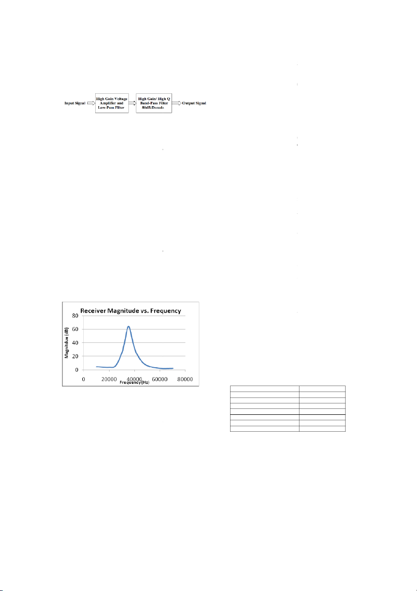
The receiver’s architecture consists of a set of narrow (high
multiplexing (OFDM) [19, 20] are now being considered for
Q) filters with high gain (Figure 10). These filters are based
higher data rate underwater applications, but the proven
on biquad band-pass filters, and essentially combine the tasks
robustness of FSK and its simplicity makes it an attractive
of filtering and amplification. The receiver is configured so
modulation scheme as the first prototype for our low-cost,
that it only amplifies signals around 35 kHz (to match the
low-power, low-data rate application.
electrical resonance frequency of the tra a nsducer) while
Reconfigurable systems (e.g., FPGAs) are a class of
attenuating low frequencies at a rate of 120dB per decade and
computing architectures that allow tradeoffs between
high frequencies at rate of 80dB per decade (Figure 11). The
flexibility and performance [21-23 ]. They strike a balance
receiver must be able to amplify only the e frequencies of
between solely hardware and solely software solutions, as they
interest because of the large amount of noise associated with
have the programmability and non-recurring engineering costs underwater acoustic signals. The current receiver
of software with performance capacity and energy efficiency
configuration consumes about 375 mW when in standby mode
approaching that of a custom hardware implementation [23].
and less than 750 mW when fully engaged. The relatively
Reconfigurable systems are known to provide the performance
high power consumption (in comparison to that of the WHOI
needed to process complex digital signal processing
Micromodem (200mW)) [7] is a result of the e receiver’s high
applications and especially provid e increased performance
gain (65dB) which is capable of sufficientl y amplifying an
benefits for highly parallel algorithms [24]. Furthermore, they
input signal as small as a few hundred microv olts allowing the
are programmable allowing the same device to be used to
receiver to pick up signals at longer distances (such as the
implement a variety of different communication protocols.
820uV received signal described in section I I). An ultra-low
Once the designs are ready in FPGA, they can relatively easily
p ower wake up circuit will be added to the receiver to
be moved to an ASIC to reduce both the area, cost and power
considerably reduce power consumption. A few receiver consumption.
component values can be changed to widen it s bandwidth (but
The following subsections describe an overview of the FSK
decrease its gain) to allow for transmission of modulation
modem implementation and its HW/SW co-design for
schemes that require more bandwidth. accurate control and I/O. A. FSK Modem Design
Table I shows the FSK modem’s time and frequency
parameters which were selected based on the properties of the
transducer. The ‘mark’ frequency represents the frequency
used to represent a digital ‘1’ when converted to baseband and
the ‘space’ frequency represents the frequency used to
represent a digital ‘0’ when conv erted to baseband. The
sampling frequency is used for sending and receiving the
modulated waveform on the carrier frequency while the
baseband frequency is used for all b b aseband processing. TABLE I. FSK MODEM PARAMETERS
Figure 11. The measured frequency response of the analog reciever Properties Assignment Modulation FSK Carrier frequency 35 KHz IV. DIGITAL TRANSCEIVER Mark frequency 1 KHz
The digital transceiver is responsible for physical layer Space frequency 2 KHz Symbol duration 5 ms
communication, i.e., implementing a su itable baseband Sampling Frequency 800 KHz processing scheme (including modulation, filtering, Baseband Frequency 16 KHz
synchronization, etc.) for the application an d d environment of
interest. There are many design choices that must be
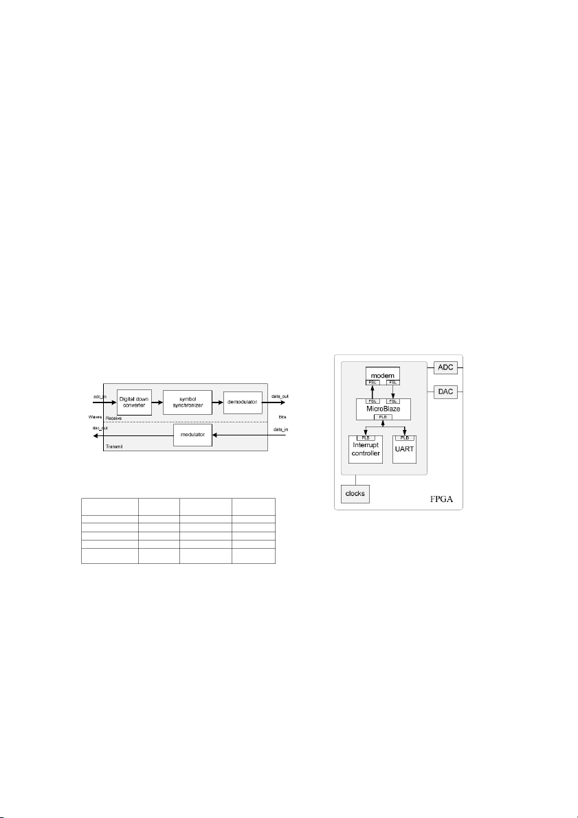
Figure 12 illustrates a block diagram of our FPGA
considered when designing a digital tra nsceiver for the
implementation of an FSK modem. In receive mode, the input
signal adc_in is the received analog signal from the analog to
with standard optimization. The resources reported for the
digital converter, sampled at the sampling frequency, which
total modem include the resources for the complete HW/SW
consists of a modulated wave form (when data is present) and
co-design as described in the next subsection (Figure 13).
noise. The following digital down converter (DDC) recovers
Using the resource values in the XPower Estimator 9.1.03, for
the signal to the digital baseband according to the FSK
an even lower power device, the Spartan-6 XC6SLX150T, the
modulation scheme and known carrier frequency and allows
power consumption estimation for the complete modem
for subsequent processing at the lower, baseband frequency. A design is 233 mW.
symbol synchronizer is then required to locate the start of the B.
first symbol of a data packet to set accurate sampling and FSK HW/SW Co-design
We used Xilinx Platform Studio 10.1 to design a HW/SW
decision timing for subsequent demodulation. The
co-design for the digital modem to allow for accurate control
synchronizer is based on correlation with a known reference
and I/O. The co-design consists of the digital modem, a
sequence (a 15-bit Gold code translated to an FSK waveform
UART (Universal Asynchronous Receiver Transmitter) to
where a ‘-1’ is represented with the space frequency and a ‘1’
connect to serial sensors or to a computer serial port for
is represented with the mark frequency). When the reference
debugging, an interrupt controller to process interrupts
and receiving sequence exactly align with each other, the
received by the UART or the modem, logic to configure the
correlation result reaches a maximum value and the
on board ADC, DAC, and clock generator, and MicroBlaze,
synchronization point is located. Details of the symbol
an embedded microprocessor to control the system (Figure 13).
synchronizer’s implementation can be found in [25]. The
The MicroBlaze processor is a 32-bit Harvard reduced
demodulator block is disabled until it obtains a valid symbol
instruction set computer (RISC) architecture optimized for
synchronization clock from the symbol synchronizer. The
implementation in Xilinx FPGAs. It interfaces to the digital
demodulator adopts a matched filter FSK demodulation
modem through two fast simplex links (FSLs), point-to-point,
scheme described making use of two bandpass filters (one
uni-directional asynchronous FIFOs that can perform fast
centered on the mark frequency and one centered on the space
communication between any two design elements on the
frequency) to decode the sequence. The decoded bit stream
FPGA that implement the FSL interface. The MicroBlaze
data_out is then sent to the host computer and translated to a
interfaces to the interrupt controller and UART core over a readable message.
peripheral local bus (PLB), based on the IBM standard 64-bit
In transmit mode, the modem receives a bit stream
PLB architecture specification.
(data_in) and modulates the bit stream into an FSK waveform
using a cosine look up table. The modulated waveform,
sampled at the sampling frequency, is sent to the analog
transceiver through the digital to analog converter (dac_out).
Figure 12. Block diagram of an FPGA implementation of an FSK modem TABLE II. FSK MODEM RESOURCES Occupied LUTs BRAMs slices Modulator 95 184 9 DDC 284 541 9
Figure 13. HW/SW Co-Design for the digital modem Demodulator 1025 1980 1 Synchronizer 12000 22101 2
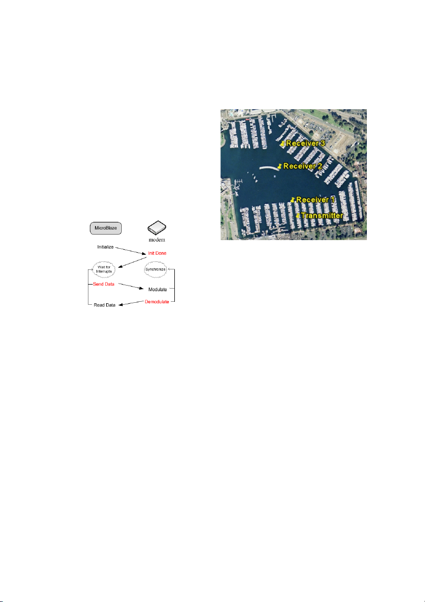
Upon start-up, the MicroBlaze initializes communication Total modem 16,706 29,076 55
with the modem by sending a command signal through the
FSL bus signaling the modem to turn on. When the modem is
ready to begin receiving signals, it sends an interrupt back to
Each component of the digital modem (modulator, digital
MicroBlaze to indicate initialization is complete. The modem
down converter, synchronizer, and demodulator) was designed
then begins the down conversion and synchronization process,
in Verilog and tested individually in ModelSim to verify its
processing the signal received from the ADC and looking for a
operation. Table II shows the FPGA hardware resources
peak above the threshold to indicate a packet has been
occupied for each component of the acoustic modem design
received. If the modem finds a peak above the threshold, it
finds the synchronization point, and demodulates the packet.
receive signal was just above 200mVpp at this distance and
The demodulated bits are stored in the FSL FIFO. When the
hence could just be detected above the converter’s noise.
full packet has been demodulated, the modem sends an
This test proved that our analog hardware could transmit a
interrupt indicating a packet has been received and the
considerable distance and would likely be able to transmit a
MicroBlaze may retrieve the packet from the FSL. The
much farther distance given a low-noise power supply at the
modem then returns to synchronization, searching for the next
receiver and further improvements to the analog transceiver. incoming packet.
After initialization, the MicroBlaze remains idle, waiting
for interrupts either from the modem or UART. If it receives
an interrupt from the modem indicating that a packet has been
demodulated, the MicroBlaze reads the bits from the FSL
FIFO and sends the bits over the UART to be printed on a
computer’s Hyperterminal for verification. If the MicroBlaze
receives an interrupt from the UART, indicating that the user
would like to send data, the MicroBlaze sends a command to
the modem to send the bitstream the MicroBlaze places in the
FSL. The modem then modulates the data from the FSL and
sends the modulated waveform to the DAC for transmission.
The MicroBlaze then returns to waiting for interrupts from the
modem or the UART and the modem returns to
synchronization, searching for the next incoming packet. This
control flow is depicted in Figure 14.
Figure 15. Mission Bay Analog Transmitter and Receiver Locations
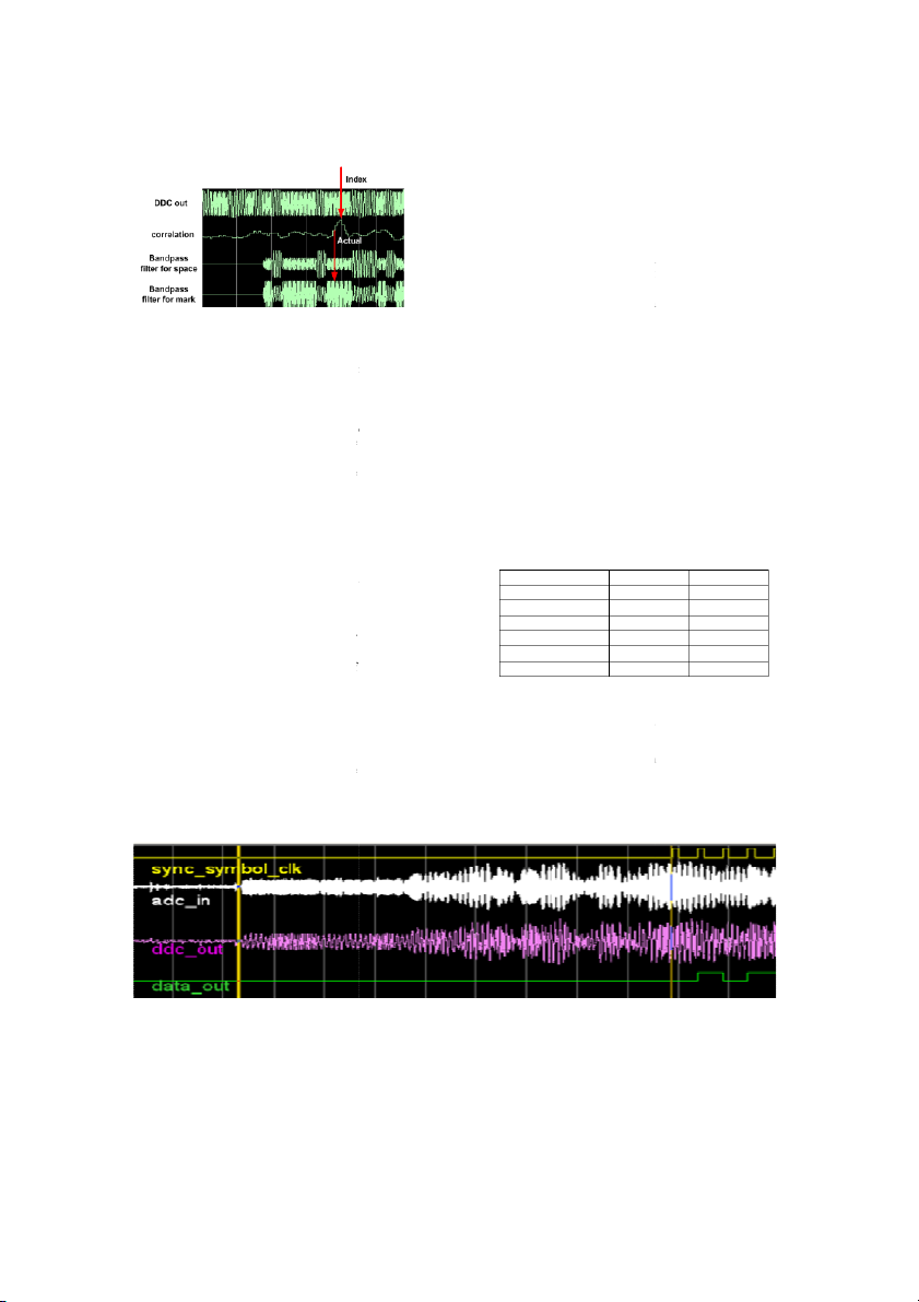
For digital testing, we purchased a prototype test
platform, the DINI DMEG-AD/DA, that includes analog to
digital and digital to analog converters, a Xilinx Virtex-4
FPGA, an onboard oscillator, and a serial port and
downloaded the HW/SW co-design to the board. We set our
initial test sequence as sending the 15 bit Gold Code of
‘011001010111101’ followed by a 100 bit packet of
randomized ones and zeros. We sent the signal through a 12
Figure 14. Modem Control Flow. Interrupts are shown in red
inch bucket of water and used the DINI board to synchronize
and demodulate the data. Figure 16 shows a snapshot of the V. INITIAL RESULTS
post place and route hardware simulation result for our digital
modem design described in Verilog HDL.
In order to verify the operation of our modem, we first
The four signals in the figure are: the output signal of the
tested the analog components (the transducer and analog
down converter (DDC out), the output of the reference cross
transceiver) and digital components (the digital transceiver)
correlation block (correlation) used for synchronization, and
separately. For the analog testing, we took our modem
the output of the two bandpass filters in the demodulator. In
hardware to Mission Bay, San Diego, CA and placed one
the DDC out signal one can observe the FSK realization of the
transceiver and transducer on the dock to act as the transmitter
Gold Code followed by the first 8 bits of data (the digital ‘0’
and placed another transceiver and transducer on a boat to act
being represented by the sparse waveform and the digital ‘1’
as the receiver. The transmitter was powered by power
being represented by the dense waveform). The bandpass
supplies on the dock and the receiver was powered by a power
filters are enabled in the demodulator when the correlation
supply connected to an inexpensive RadioShack AC/DC
result first rises above the threshold (not shown). The vertical
converter that unfortunately produced a substantial amount of
arrow labeled “Index” illustrates the synchronized peak found noise (200mVpp).
by the hardware which is a known clock delay from the start
We sent a 35kHz sinusoid from the transmitter to the
of the data (vertical arrow labeled “Actual”). The bit stream
receiver placed at three different locations as shown in Figure
demodulated from the “Actual” peak are sent to the FSL
15: 1. 75 meters, 2. 235 meters, and 3. 350 meter away. We
buffer to be read by the MicroBlaze and printed to the
were able to successfully detect the signal at 350m by
Hyperterminal. The bits written to the Hyperterminal revealed
applying 66Vrms across the transmit transducer, however the
0% error rate for the 100 bit packet from the 12 inch plastic
b ucket. The test was repeated with different data bits 10 times
It can easily be seen in Figure 17 that the data can be all producing 0% error.
accurately demodulated for the first few symbols of the
received packet as there is a clear distinction between the
mark and space frequencies. However, a strong multipath
arrives at the receiver after about the 7th symbol, severely
distorting the signal making accurate demodulation impossible.
Concrete pools are one of the most difficult underwater
channels due to extremely strong multipath and most other
underwater acoustic modems fail in this environment.
Although we obtained 30% erro r rate in the concrete pool,
we were encouraged by the results and are confident in an
environment with less severe multipath, the modem can
Figure 16. Snapshot of hardware simula tion result for
perform well. We are currently developing a power supply 12” bucket test
board, battery pack, and waterrtight housing (that can
withstand pressures at depth of up to 100m) so we can test our
Because the bucket produced such pe rfect data, we
modem in the open ocean in order to assess its true
generated data in Matlab with packet lengths of 10000 performance.
symbols and sent the signals to the hardware for
synchronization and demodulation. These packets achieved a
VI. MODEM COMPARISON AND CONCLUSION
bit error rate of 10-2 at 10dB SNR.
Our anticipated cost and power estimates for the full
Feeling confident that our analog and digital hardware
modem prototype (not including batteries or housing) are
components worked properly, we conducte d an initial full
shown in Table III. The power consumption of the analog
system test at the UCSD Canyon View poo l, a 50m x 25m
transceiver depends on its mode. The interfaces (ADC and
concrete pool with 1m depth on the shallow e nd and 5m depth
DAC) are specified as TBD (to be determined) as the ADC
on the deep end. As the pool provided outdo or power outlets,
and DAC on our evaluation board are over specified and too
we were able to power both the transmitter and receiver off
power consuming for our intended design. power supplies.
At 50 meters distance, we sent a packet of 400 symbols TABLE III.
followed by a 400 symbol clearing period followed by another
COST AND POWER ESTIMATES FOR THE
p acket of 400 symbols using only 6.5Vrms across the transmit UNDERWATER MODEM
transducer. The transducers were submerged to a depth of 10 Cost ($) Power (W)
cm and placed along the 50m side of the pool to avoid Transducer 50 N/A
swimmers. The digital hardware was able to successfully Transceiver 125 1- 40
detect the start of each packet, but failed to accurately Digital Components 75 0.2
demodulate the data, achieving 30% bit error rate. Figure 17 Power Supply 100 TBD
shows the first few symbols of the first received packet, at Interfaces TBD TBD
10dB SNR, starting with the 15 symbol ref f erence sequence Total ~$250
followed by four data bits. The bold yellow v ertical bar marks
the start of the reference sequence (easily seen above the
We compare our design with three commercial modems,
initial noise) and the light yellow vertical bar denotes what the
two designed at private firms (LinkQuest and Teledyne
synchronizer determined to be the start of data.
Benthos) and one designed at Woods Hole Oceanographic
Sync_symbol_clk denotes the symbol clock synchronized to
Institute in Table IV. Note that the distance and bit rates
the start of the first data symbol. Adc_in shows the input to
reported for the modems are the maximum distance and rates
the ADC, ddc_out shows the downconvert e e d, downsampled
achievable under ideal conditions. Also note that the price of
signal used for all digital processing and data_out shows the
the commercial modem designs is based on market prices demodulated bits.
whereas our design cost is based solely on parts costs and
assembly labor. However the parts price of the commercial
Figure 17. Snapshot of 50m Canyon Pool Test Results
TABLE IV. UNDERWATER ACOUSTIC MODEM COMPARISON Transmission Transmit & Firmware and software Data rate Cost distance Receive power design Teledyne 12 W 2400 bps 2-6 km $10,000 Proprietary Benthos 0.4 W 4 W LinkQuest 9600 bps 1500 m $8,000 Proprietary 0.8 W 80 bps (FH- WHOI FSK) 10-100 W All design information Micro- 1-10 km $8,000 300-5400 200 mW – 2W is available online. Modem (PSK) UCSD 1 – 40 W All design information 200 bps 2 km $600 Modem 1W will be available online.
modems is still much more than the full price of our modem as
[8] R. A. Iltis, H. Lee, R. Kastner, D. Doonan, T. Fu, R. Moore, and M.
commercial transducers used in the designs solely cost a few
Chin, "An Underwater Acoustic Telemetry Modem for Eco-Sensing," thousand dollars.
Proceedings of MTS/IEEE Oceans, 2005.
[9] DSP Implementation of OFDM: H. Yan, S. Zhou, Z. Shi, and B. Li, “A
From this comparison we observe that our modem currently
DSP implementation of OFDM acoustic modem,” in Proceedings of
stands as low-cost, comparable power alternative to existing
ACM International Workshop on Underwater Networks, 2007.
modem designs. In the future, to further reduce power
[10] Jurdak, R.; Aguiar, P.; Baldi, P.; Lopes, C.V., "Software Modems for
consumption, we plan to explore the possibilities to provide
Underwater Sensor Networks," OCEANS 2007 - Europe vol., no., pp.1-6, 18-21 June 2007
signal detection at even lower power levels. This is paramount
[11] B. Benson, G. Chang, D. Manov, B. Graham, and R. Kastner, "Design
to building a modem that has low listening power, which is
of a low-cost acoustic modem for moored oceanographic applications,"
also a key requirement to ensure long lifetime on a limited
Proceedings of ACM International Workshop on Underwater Networks,
battery supply. We plan to eventually utilize a design that has 2006.
[12] Sherman, C.H.; Butler, J.L.Transducers and Arrays for Underwater
a programmable gain, which is dynamically controlled by the
Sound. New York : Springer, 2007.
digital hardware platform. In addition, further changes to the
[13] Cytec Industries. http://www.cytec.com.
circuit design of the transceiver will be made to further
[14] Wilson, O.B. An Introduction to Theory and Design of Sonar
increase its efficiency and digital transceiver implementations
Transducers. Peninsula Pub, 1985.
[15] Revision of DOD-STD-1376A, Ad Hoc Subcommittee Report on
of advanced modulation techniques will be explored. Piezoceramics (1 APRIL 1986).
[16] ITC-1042. Deep Water Omnidirectional Transducer. http://www.itc- ACKNOWLEDGMENT
transducers.com/itc_page.asp?productID=11&type=3&subtypename=Ca
This work was supported in part by the China Scholarship
libration%20Standards&headline=Calibration%20Standards
[17] Morgan ElectroCeramics. http://www.morganelectroceramics.com
Council, National Science Foundation Grant #0816419 and a
[18] Kilfoyle D. B., Baggeroer A. B. 2000. “The State of the Art in
National Science Foundation Graduate Research Fellowship.
Underwater Acoustic Telemetry”, IEEE Journal of Oceanic Engineering,
We would like to thank Douglas Palmer, Diba Mirza, John Vol. 25, No.1, (January 2000)
Hildebrand, Feng Tong, Brent Hurley for their assistance and
[19] Yan H., Zhou S., Shi Z., and Li B. 2007. “A DSP implementation of
OFDM acoustic modem”, In Proc. of the ACM International Workshop support with this project.
on Underwater Networks (WUWNet), (Montreal, Quebec, Canada, September 14, 2007) REFERENCES
[20] Kang T. and Litis R. A. 2008. “Matching Pursuits Channel Estimation for
an Underwater Acoustic OFDM Modem” In Proc. of the 2008 IEEE
[1] Grund, M.; Freitag, L.; Preisig, J.; Ball, K., "The PLUSNet Underwater
International Conference on Acoustics, Speech, and Signal Processing Communications System: Acoustic Telemetry for Undersea
Surveillance," OCEANS 2006
Special Session on Physcial Layer Challenges in Underwater Acoustic
[2] R. Jurdak, C. V. Lopes and P. Baldi. Battery Lifetime Estimation
Communications, (Las Vegas, Nevada, April 2008)
And Optimization for Underwater Snsor Networks. Sensor Network
[21] K. Bondalapati and V. K. Prasanna, "Reconfigurable computing
Operations, Wiley/IEEE Press. May, 2006.
systems," Proceedings of the IEEE, vol. 90, pp. 1201-17, 2002.
[3] J. Wills, W. Ye, and J. Heidemann, "Low-power acoustic modem for
[22] K. Compton and S. Hauck, "Reconfigurable computing: a survey of
dense underwater sensor networks," Proceedings of ACM International
systems and software," ACM Computing Surveys, vol. 34, pp. 171-210,
Workshop on Underwater Networks, 2006. 2002.
[4] J. Jaffe and C. Schurgers, "Sensor networks of freely drifting
[23] R. Kastner, A. Kaplan, and M. Sarrafzadeh, Synthesis Techniques and
autonomous underwater explorers," Proceedings of ACM International
Optimizations for Reconfigurable Systems. Boston: Kluwer Academic,
Workshop on Underwater Networks, 2006. 2004.
[5] Brooks, Andy. Deputy Program Director, Moorea Coral Reef LTER.
[24] R. Tessier and W. Burleson, "Reconfigurable computing for digital signal
Personal Correspondence August 24, 2009.
processing: a survey," Journal of VLSI Signal Processing Systems for
[6] J. Heidemann, Y. Li, A. Syed, J Wills and W. Ye, "Research
Signal, Image, and Video Technology, vol. 28, pp.7-27, 2001.
Challenges and Applications for Underwater Sensor Networking",
[25] Y. Li, B. Benson, X. Zhang, and R. Kastner. “Hardware Implementation
Proceedings of the IEEE Wireless Communications and Networking
of Symbol Synchronization for Underwater FSK.” IEEE International Conference (WCNC2006), 2006.
Conference on Sensor Networks, Ubiquitous, and Trustworthy
[7] L. Freitag, M. Grund, S. Singh, J. Partan, and P. Koski, "The WHOI Computing, 2010.
Micro-Modem: An acoustic communications and navigation system for
multiple platforms," in IEEE Oceans Europe. 2005.
Tài liệu liên quan:
-

Đề cương môn công nghệ web- Trường Đại học bách khoa - Đại học đà nẵng.
84 42 -
Đề cương môn công nghệ web- Trường Đại học bách khoa - Đại học đà nẵng.
57 29 -

Đề cương môn công nghệ web- Trường Đại học bách khoa - Đại học đà nẵng.
71 36 -

Đề cương môn công nghệ web- Trường Đại học bách khoa - Đại học đà nẵng.
67 34 -

Đề cương môn công nghệ web- Trường Đại học bách khoa - Đại học đà nẵng.
62 31