Gain-Enhancement Differential Amplifier Using Positive Feedback
Gain-Enhancement Differential Amplifier Using Positive Feedback. Tài liệu được sưu tầm giúp bạn tham khảo, ôn tập và đạt kết quả cao. Mời bạn đọc đón xem.
Môn: Tài liệu Tổng hợp 3.6 K tài liệu
Trường: Tài liệu khác 3.9 K tài liệu
Tác giả:
Preview text:
Gain-Enhancement Differential Amplifier Using Positive Feedback
Phuoc T. Tran, Herbert L. Hess, Kenneth V. Noren, Suat Ay
University of Idaho, Moscow, Idaho, U.S.A.
Abstract—This paper presents a differential amplifier design
In addition, the new design circuit has a built-in tuning
with gain enhancement using positive feedback. Comparing
strategy for an adjustable gain or tuning out the process-
with the standard complementary metal-oxide-semiconductor
voltage-temperature variations.
(CMOS) differential amplifier, the new circuit has improved
specifications, such as higher small-signal voltage gain, output
This paper is organized as follows: Section II discusses a
voltage swing, and large bandwidth. In addition, the circuit has
a built-in tuning capability for adjustable gain or tuning out the
conventional CMOS differential amplifier with a gain
process-voltage-temperature (PVT) variations. This paper also
equation and its relationship between ro , L , and sat , DS V of a
presents a comparison of noise and power dissipation that was
MOSFET. Section III introduces the basic theory of positive
performed using Spice simulations.
feedback system. Sections IV presents the new design
circuit. Section V shows the advantages of the new circuit.
Key words: gain enhancement, positive feedback, cross-coupled, differential amplifier
Section VI provides simulation results and is followed by the conclusion in Section VII. I. INTRODUCTION II. CMOS DIFFERENTIAL AMPLIFIER
In CMOS technology, the size for the gate channel length
of complementary MOS transistors has been reduced from
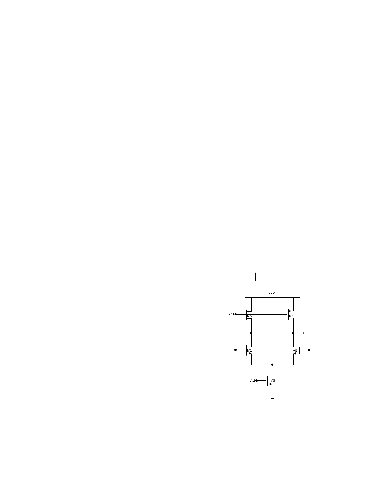
The circuit in Fig. 1 is a conventional CMOS differential
micrometers to submicron, which is known as short channel. amplifier in analog circuits [1] – [2]. The circuit is used to
One of the most problematic issues with integrated circuit provide a voltage gain, which heavily depends on the output
(IC) is scaling down the gate channel length of the transistor resistance of both PMOS and NMOS transistors. The output
devices for low-voltage, which poses a significant problem resistance in turn depends on channel length of MOSFET’s.
for analog circuits. Scaling down devices to submicron or The gain equation of the differential amplifier in Fig. 1 can be
smaller levels means lowering the output resistance of the written as
MOSFET; as a result, the small-signal gain of the differential pair is reduced [1] – [3]. AV g ,1 m 2 on r || op r (1)
To recover that small-signal gain, the output resistance is
increased by arranging the MOSFET devices vertically,
which this is known as cascode [1] – [2]. Cascoding
increases the differential gain significantly, but it also causes
a reduction in the overhead voltage. Consequently, this
reduces the output signal swings of the differential amplifiers. 1o o2
This paper addresses the problems of gain decrease and
output signal swing reduction by representing the concept of 1i
a cross-coupled differential pair with a positive feedback. i2
This concept provides an alternative solution with significant
advantages. The cross-couple differential pair means having
the MOSFET devices configured laterally rather than
vertically for the differential pair’s gain enhancement. Thus,
the laterally configured amplifier circuit increases the small-
signal voltage gain and also preserves the higher output voltage swings.
Figure 1 A Conventional CMOS diff-amp circuit
978-1-4673-2527-1/12/$31.00 ©2012 IEEE 718
From [1], the relationship between r
IV. GAIN-ENHANCEMENT CROSS-COUPLED o , L , and sat , DS V for
a MOSFET device operating in the saturation region is DIFF-AMP CIRCUIT
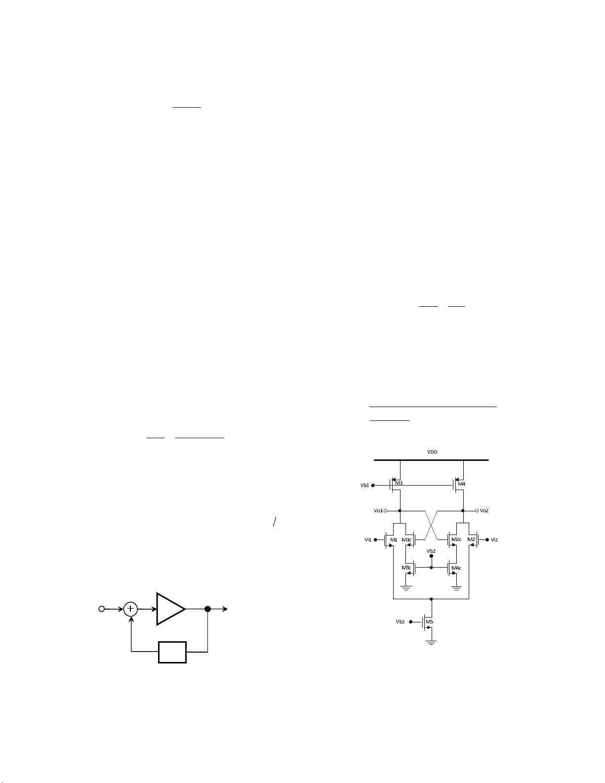
The topology circuit in Fig. 3 proposes with of the 2 L r
concept using of uses positive feedback strategy. The o (2) 2 V
proposed circuit is a fully-symmetric differential amplifier, , DS sat
which has the cross-coupled MOS transistors that feedback
Based on (2), a shorter channel length MOSFET yields between the input and the output nodes. This circuit’s cross-
lesser output resistance. Therefore, the small-signal gain of coupling is “horizontal” rather than “vertical”, and it
that diff-amp is also smaller.
generates a negative transconductance, g . At the output m
nodes, the negative conductance cancels the positive output III. POSITIVE FEEDBACK SYSTEM
conductance of the PMOS load transistors and NMOS
differential-pair. As a result, a very high DC gain of the
Positive feedback in analog circuits has not been as differential amplifier is generated.
widely used as negative feedback systems because it was
believed that positive feedback results in unstable and
To derive the small-signal gain equation for the new
uncontrollable system. However, if the circuit with the design circuit, let us focus on the center part of the circuit
positive feedback is designed properly, the system is displayed in Fig. 4, which is a pair of cross-couple controllable [4].
MOSFETs. The short circuit transconductance equation can be defined as
Moreover, positive feedback can be beneficial for gain
enhancement circuits [4] - 8]. Because the intrinsic gain of Io Io
MOS transistors has been degraded significantly in scaled- Gm (4) V V
down technologies, a positive feedback can provide a solution c 1 g o2
to the increase in small-signal gain. Several papers have been
published describing how positive feedback enhances the
By using the small-signal model, the short-circuit amplifier gain [4] - [8].
transconductance of the cross-couple MOSFETs is being analyzed as follows:
Fig. 2 shows the schematic diagram of a positive feedback
system. The quantity A i s the feed forward amplifier Solve for G m
network. The quantity B is the feedback network. g c 1 m
The expression for the transfer ratio in Fig. 2 is as follows: G m r (5) c 1 o o r 3c g c1 m ro3c g c 1 mb ro c 3 Ys As r c 1 o (3) Xs 1 As s The As
s term is the “loop gain” of the system. The
loop gain values must be greater than zero but less than one
to ensure the feedback is positive. When the loop gain As
s is equal to one, the denominator of (3) becomes
zero; thus, the value of the transfer function Ys Xs
becomes infinity. At this point, the pole is moved to the
right-half plane, and the circuit becomes unstable. Also,
designing too close to the origin of the axes i s not
recommended because of the instability concern. Xs A s Ys s
Figure 3 Gain-enhancement diff-amp using positive feedback
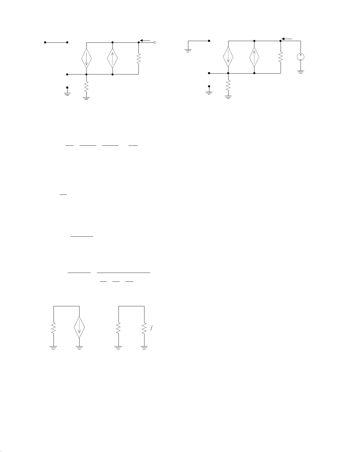
Figure 2 Diagram of positive feedback system 719 I i o t c 1 g o2 c 1 g o2 1 o g g r g g c 1 mb c 1 sb r V c 1 m 1 gs c 1 mb c 1 sb c 1 m 1 gs t c 1 o c 1 o s c 1 c 1 s c 1 b r c 1 b r o3c o3c
Figure 4 Small-signal model of cross-couple MOSFETs which is used to
Figure 6 Small-signal model of cross-couple MOSFETs derive Gm
used to derive output resistance with a test voltage V. ADVANTAGES
Using the equivalent circuit in Fig. 5, R can be written as
These are a number of advantages related to the new 1 o 1 o o2 1 R (6)
design cross-coupled differential amplifier circuit. One of the Io Gmo2 Gmo2 Gm
advantages that is that the circuit has a wider output voltage
swing, approximately ten percent better compared that to
The next step is to determine the output resistance of a known published positive feedback circuits in [5] – [7].
cross-coupled circuit by using a test voltage, which is shown
in Fig. 6. The output resistance, R
First, from the circuit in Fig. (1) and other circuits in [5] – o, can be solved as
[7], for a minimum voltage swing, the voltage swing is the V
same for all compared circuits. t R o r c 1 o ro3c g c 1 m g c 1 mb r c1 o ro3c (7) i t min V OV V (10)
Thus, the overall transfer function of small-signal gain is
However, the maximum voltage swing of the literature given by
circuits is reduced by a threshold voltage from where V DD is. Its equation is written as V V A o2 1 o g d 1 m r || r || R || R 1 o o3 o (8) Vid max V DD V THp V (11) which also can be rewritten as
For the circuit concept presented in this paper, the
maximum voltage swing is higher because the P-channel V V g A o2 1 o 1 m
MOSFETs only require to lower by an overdrive voltage, d (9) id V 1 1 1
which is several times lower than a threshold voltage. The G m equation can be written as r 1 o o r 3 R o max V DD V OV V (12) 1 o 2 o
Thus, the range of the voltage swing of the literature
circuits is lower compared to that of the new gain
enhancement cross-coupled circuit. R o G 1 G m o2 Ro m
An additional advantage of the circuit is a built-in tuning
strategy that can be used for an adjustable gain. With the adjustable bias voltage, b
V 2 , it can set the circuit up for
Figure 5 Equivalent circuit of transconductance, G
different levels of desirable voltage gain. See Fig. 3. m b V 2
is connected to the gates of the NMOS transistors M1b and
M2b, which are positioned below the cross-couple circuit. The voltage of b
V 2 essentially keeps M3c and M4c devices
operating in saturation and determines the output resistance
of the cascade current mirror. For a different value of b V 2 , a 720
different output resistance is generated at the drains of the
cross-couple circuit. A different voltage gain is produced. VII. CONCLUSION
Finally, the advantage of the new design circuit is that the
The new diff-amp with positive feedback circuit has an same
improved small-signal gain like other published positive b
V 2 bias voltage of the circuit that was used for
adjusting voltage gain can also be used to compensate for the feedback circuits. The new diff-amp has a preserved high
effects of the process, voltage, and temperature variations. voltage swing and has a large gain bandwidth. The new
For example, if the circuit experiences process, voltage, or circuit also has a built-in tuning strategy for an adjustable
temperature variation, the variation can cause a significant gain or tuning out the PVT variations. The penalty of noise
change in threshold voltage and result in a different voltage and unity gain is higher compared to a standard CMOS diff-
gain, which can cause serious problems for any system. To amp.
tune out or compensate for this variation effect, the voltage of b
V 2 is adjusted to a value where the circuit can restore its REFERENCES
voltage gain to the previous level. [1]
R. Jacob Baker, “CMOS: Circuit Design, Layout, and Simulation,”
Wiley-IEEE Press, 2nd Edition, 2005. [2]
B. Razavi, “Design of Analog CMOS Integrated Circuits,” VI. SIMULATION RESULTS McGraw-Hill Edition, 2001. [3]
M. Pude, C. Macchietto, P. Singh, J. Burleson, P.R. Mukund,
The characteristics of the two diff-pair circuits are
“Maximum Intrinsic Gain Degradation in Technology Scaling,”
compared as follows: a standard CMOS diff-amp in Fig. 1
Semiconductor Device Research Symposium, 2007 International, pp. 1-2, 20007.
and a diff-amp with positive feedback circuit presented in this [4]
M.E. Schlarmann, S.Q. Malik, R.L. Geiger, “Positive Feedback
paper. All circuits were designed with same power
Gain-Enhancement Techniques for Amplifier Design,” IEEE
consumption and 1.0V supply voltage in the IBM 90nm
International Symposium on Circuits and Systems, Volume 2, May
CMOS process and were simulated using LT Spice. The 2002. [5]
M. M. Amourah, R. L. Geiger, "All digital transistor high gain
simulations results are shown in Table I, where the DC-gain
operational amplifier using positive feedback technique," Circuits
of a diff-amp with positive feedback circuit is higher than that
and Systems, 2002. ISCAS 2002. IEEE International Symposium on
of a standard CMOS diff-amp circuit, but its noise volume 1, pp. I-701 - I-704.
performance and unity gain frequency are less favorable [6]
M.M. Amourah, R.L. Geiger, “A High Gain Strategy with Positive-
Feedback Gain Enhancement Technique,” IEEE International
compared to a standard CMOS diff-amp.
Symposium on Circuits and Systems, pp. 631-634, May 2001. [7]
R. Wang, R. Harjani, “Partial Positive Feedback for Gain
TABLE I Comparison of diff-amp’s characteristics
Enhancement of Low-Power CMOS OTAs,” Analog Integrated Circuit Standard CMOS Diff-amp with positive
Circuits and Signal Processing, Special issue, Vol. 8 Issue 1, pp. characteristics diff-pair feedback 21–35, July 1995. Supply voltage 1.0V 1.0V [8]
M. Pude, P. R. Mukund, P. Singh, K. Paradis, J. Burleson,, Power dissipation 10 W 10 W
“Amplifier Gain Enhancement with Positive Feedback,” Circuits
and Systems (MWSCAS), 2010 53rd IEEE International Midwest Gain 39dB 59dB
Symposium, PP 981 – 984. Output noise (10 KHz) 0.9 mV Hz 10.4 mV Hz Phase margin 90.5o 89.7o Unity gain freq. 23GHz 3.5GHz 721
Tài liệu liên quan:
-

Ung dung game hoa trong cac chien dich MKT
18 9 -

Bao cao Chi so TMDT Viet Nam 2025
15 8 -
Thông tư quy định về việc phân quyền, phân cấp và phân định thẩm quyền quản lý nhà nước về giáo dục cho chính quyền địa phương
24 12 -
Nghị quyết về phát huy các giá trị di sản văn hóa gắn với phát triên du lịch bền vững tỉnh Khánh Hòa đến năm 2025, định hướng đến năm 2030
14 7 -
Quyết định phê duyệt Chiến lược phát triển du lịch Việt Nam đến năm 2030
13 7