Hamming Code and Error Correction Techniques in Memory Systems | Môn Kiến trúc máy tính 1 - Đại học Xây Dựng Hà Nội
Hamming Code and Error Correction Techniques in Memory Systems Môn Kiến trúc máy tính 1. Tài liệu được sưu tầm gồm 14 trang, giúp bạn ôn tập tốt hơn. Mời các bạn đón xem.
Môn: Kiến trúc máy tính 1 (structural analysys 1) 23 tài liệu
Trường: Trường Đại học Xây Dựng Hà Nội 540 tài liệu
Tác giả:


Preview text:
lOMoAR cPSD| 58970315
Figure 5.8 Hamming Error-Correcting Code
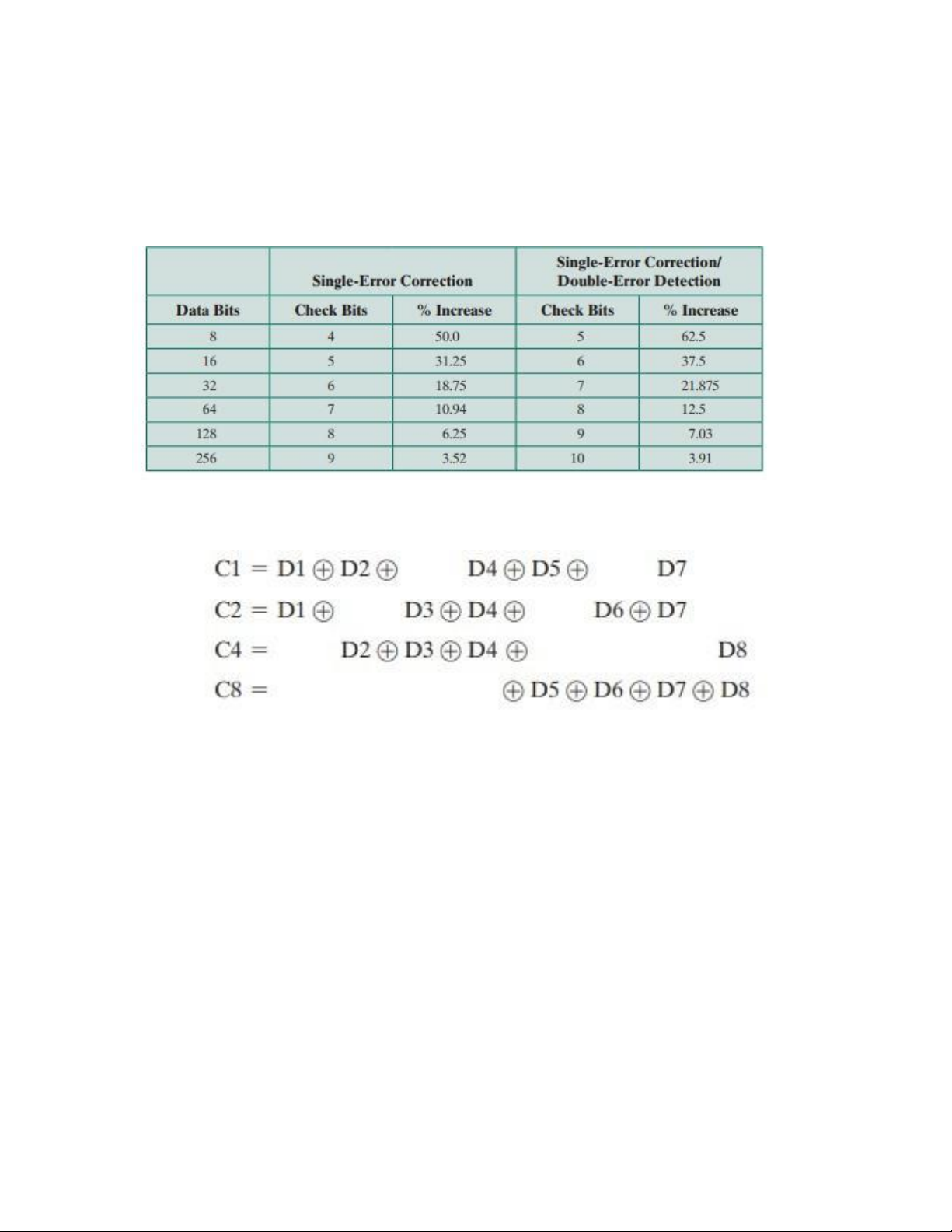
Thus, eight data bits require four check bits. The first three columns of Table 5.2 lists
the number of check bits required for various data word lengths.
For convenience, we would like to generate a 4-bit syndrome for an 8-bit data word
with the following characteristics:
■If the syndrome contains all Os, no error has been detected.
■ If the syndrome contains one and only one bit set to 1, then an error has occurred
in one of the 4 check bits. No correction is needed.
■ If the syndrome contains more than one bit set to 1, then the numerical value of the
syndrome indicates the position of the data bit in error. This data bit is inverted for correction. lOMoAR cPSD| 58970315
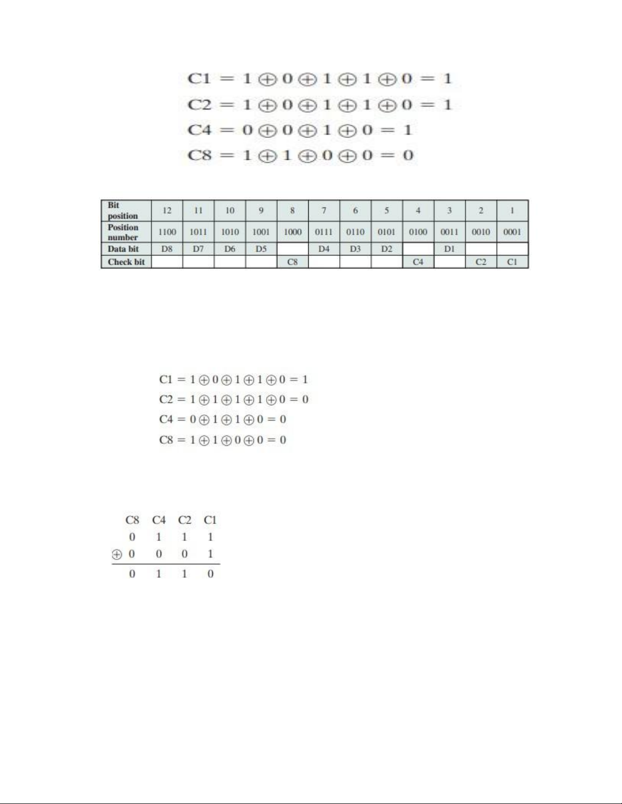
To achieve these characteristics, the data and check bits are arranged into a 12-bit
word as depicted in Figure 5.9. The bit positions are numbered from 1 to 12. Those
bit positions whose position numbers are powers of 2 are designated as check
178 CHAPTER 5/ INTERNAL MEMORY
Table 5.2 Increase in Word Length with Error Correction
bits. The check bits are calculated as follows, where the symbol designates the exclusive-OR operation:
Each check bit operates on every data bit whose position number contains a 1 in the
same bit position as the position number of that check bit. Thus, data bit pos-itions
3, 5, 7, 9, and 11 (D1, D2, D4, D5, D7) all contain a 1 in the least significant bit of
their position number as does C1; bit positions 3, 6, 7, 10, and 11 all contain a 1 in
the second bit position, as does C2; and so on. Looked at another way, bit position n
is checked by those bits C such that ∑ = n. For example, position 7 is checked by₁
bits in position 4, 2, and 1; and 7 = 4+2+1.
Let us verify that this scheme works with an example. Assume that the 8-bit input
word is 00111001, with data bit D1 in the rightmost position. The calculations are as follows: lOMoAR cPSD| 58970315
Figure 5.9 Layout of Data Bits and Check Bits 5.2/ERROR CORRECTION
Suppose now that data bit 3 sustains an error and is changed from 0 to 1. When the
check bits are recalculated, we have
When the new check bits are compared with the old check bits, the syndrome word is formed:
The result is 0110, indicating that bit position 6, which contains data bit 3, is in error.
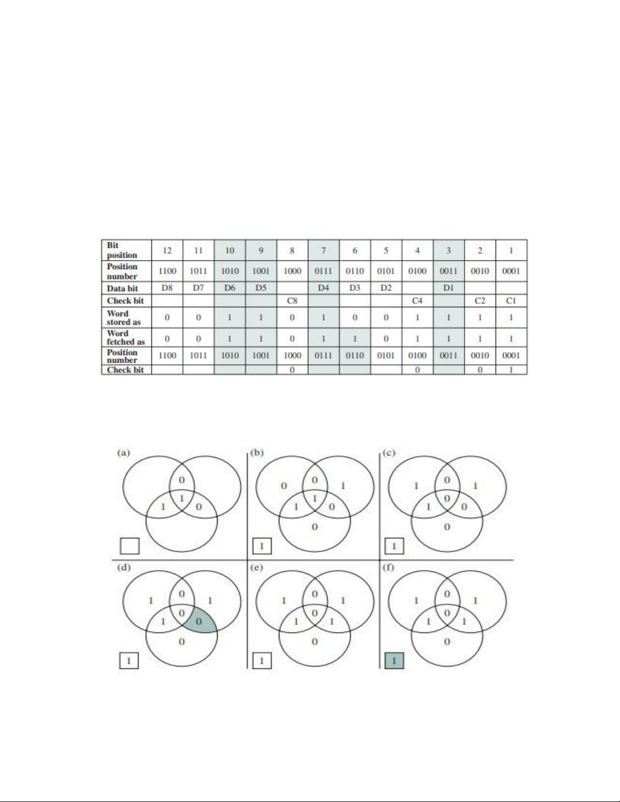
Figure 5.10 illustrates the preceding calculation. The data and check bits are
positioned properly in the 12-bit word. Four of the data bits have a value 1 (shaded
in the table), and their bit position values are XORed to produce the Hamming code
0111, which forms the four check digits. The entire block that is stored is
001101001111. Suppose now that data bit 3, in bit position 6, sustains an error and
is changed from 0 to 1. The resulting block is 001101101111, with a Hamming code
of 0001. An XOR of the Hamming code and all of the bit position values for nonzero lOMoAR cPSD| 58970315
data bits results in 0110. The nonzero result detects an error and indicates that the error is in bit position 6.
The code just described is known as a single-error-correcting (SEC) code. More
commonly, semiconductor memory is equipped with a single-error-correcting,
double-error-detecting (SEC-DED) code. As Table 5.2 shows, such codes require one
additional bit compared with SEC codes.
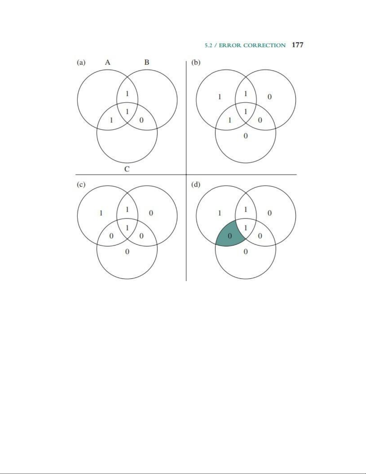
Figure 5.11 illustrates how such a code works, again with a 4-bit data word. The
sequence shows that if two errors occur (Figure 5.11c), the checking procedure goes
astray (d) and worsens the problem by creating a third error (e). To overcome
Figure 5.10 Check Bit Calculation 180 CHAPTER 5/INTERNAL MEMORY
Figure 5.11 Hamming SEC-DEC Code
the problem, an eighth bit is added that is set so that the total number of 1s in the
diagram is even. The extra parity bit catches the error (f). lOMoAR cPSD| 58970315
An error-correcting code enhances the reliability of the memory at the cost of added
complexity. With a 1-bit-per-chip organization, an SEC-DED code is generally
considered adequate. For example, the IBM 30xx implementations used an 8bit SEC-
DED code for each 64 bits of data in main memory. Thus, the size of main memory
is actually about 12% larger than is apparent to the user. The VAX computers used a
7-bit SEC-DED for each 32 bits of memory, for a 22% overhead. Contemporary
DRAM systems may have anywhere from 7% to 20% overhead [SHAR03]. 5.3 DDR DRAM
As discussed in Chapter 1, one of the most critical system bottlenecks when using
high-performance processors is the interface to internal main memory. This interface
is the most important pathway in the entire computer system. The basic building
block of main memory remains the DRAM chip, as it has for decades; until recently,
there had been no significant changes in DRAM architecture since the early 1970s.
The traditional DRAM chip is constrained both by its internal architecture and by its
interface to the processor's memory bus.
We have seen that one attack on the performance problem of DRAM main memory
has been to insert one or more levels of high-speed SRAM cache between the DRAM
main memory and the processor. But SRAM is much costlier than DRAM, and
expanding cache size beyond a certain point yields diminishing returns.
In recent years, a number of enhancements to the basic DRAM architecture have
been explored. The schemes that currently dominate the market are SDRAM and
DDR-DRAM. We examine each of these in turn. Synchronous DRAM
One of the most widely used forms of DRAM is the synchronous DRAM (SDRAM).
Unlike the traditional DRAM, which is asynchronous, the SDRAM exchanges data
with the processor synchronized to an external clock signal and running at the full
speed of the processor/memory bus without imposing wait states.
In a typical DRAM, the processor presents addresses and control levels to the
memory, indicating that a set of data at a particular location in memory should be
either read from or written into the DRAM. After a delay, the access time, the DRAM
either writes or reads the data. During the access-time delay, the DRAM performs
various internal functions, such as activating the high capacitance of the row and
column lines, sensing the data, and routing the data out through the output buff-ers.
The processor must simply wait through this delay, slowing system performance. lOMoAR cPSD| 58970315
With synchronous access, the DRAM moves data in and out under control of the
system clock. The processor or other master issues the instruction and address
information, which is latched by the DRAM. The DRAM then responds after a set
number of clock cycles. Meanwhile, the master can safely do other tasks while the
SDRAM is processing the request.
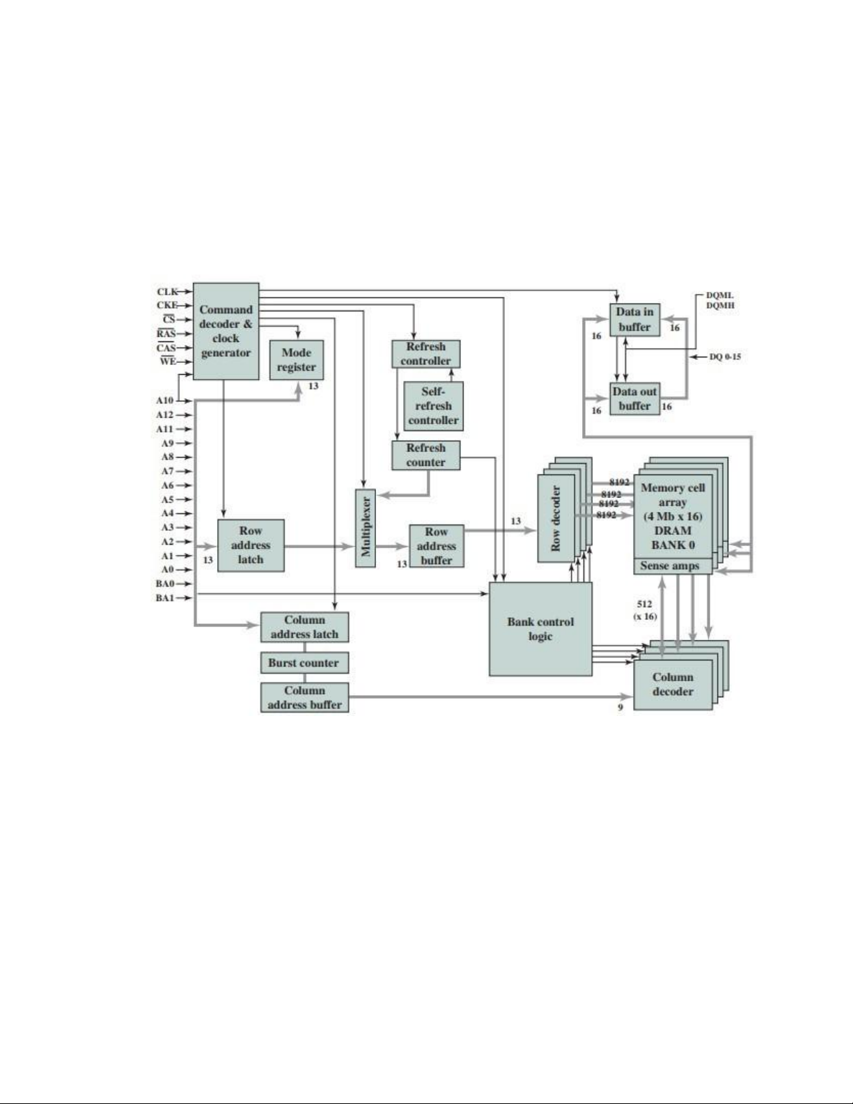
Figure 5.12 shows the internal logic of a typical 256-Mb SDRAM typical of
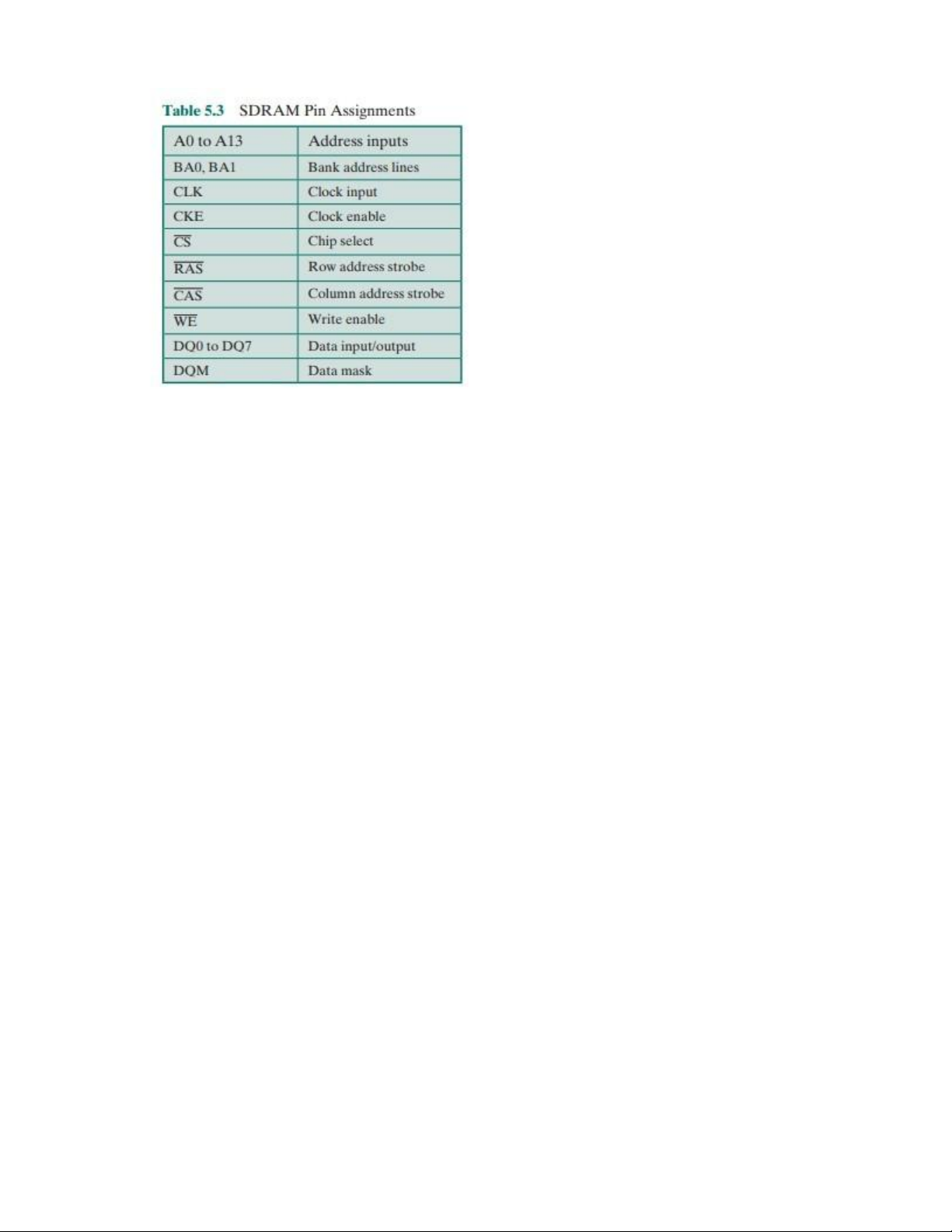
SDRAM organization, and Table 5.3 defines the various pin assignments. The
Figure 5.12 256-Mb Synchronous Dynamic RAM (SDRAM) 182 CHAPTER 5/ INTERNAL MEMORY lOMoAR cPSD| 58970315
SDRAM employs a burst mode to eliminate the address setup time and row and
column line precharge time after the first access. In burst mode, a series of data bits
can be clocked out rapidly after the first bit has been accessed. This mode is useful
when all the bits to be accessed are in sequence and in the same row of the array as
the initial access. In addition, the SDRAM has a multiple-bank internal architecture
that improves opportunities for on-chip parallelism.
The mode register and associated control logic is another key feature differentiating
SDRAMs from conventional DRAMs. It provides a mechanism to customize the
SDRAM to suit specific system needs. The mode register specifies the burst length,
which is the number of separate units of data synchronously fed onto the bus. The
register also allows the programmer to adjust the latency between receipt of a read
request and the beginning of data transfer.
The SDRAM performs best when it is transferring large blocks of data sequentially,
such as for applications like word processing, spreadsheets, and multimedia. Figure
5.13 shows an example of SDRAM operation. In this case, the burst length is 4 and
the latency is 2. The burst read command is initiated by having CS and CAS low
while holding RAS and WE high at the rising edge of the clock. The address inputs
determine the starting column address for the burst, and the mode register sets the
type of burst (sequential or interleave) and the burst length (1, 2, 4, 8, full page). The
delay from the start of the command to when the data from the first cell appears on
the outputs is equal to the value of the CAS latency that is set in the mode register. DDR SDRAM
Although SDRAM is a significant improvement on asynchronous RAM, it still has
shortcomings that unnecessarily limit that I/O data rate that can be achieved. To
address these shortcomings a newer version of SDRAM, referred to as double- lOMoAR cPSD| 58970315
datarate DRAM (DDR DRAM) provides several features that dramatically increase
the data rate. DDR DRAM was developed by the JEDEC Solid State Tech-nology Association, the Electronic Industries Alliance's semiconductor-
engineeringstandardization body. Numerous companies make DDR chips, which are
widely used in desktop computers and servers.
DDR achieves higher data rates in three ways. First, the data transfer is synchronized
to both the rising and falling edge of the clock, rather than just the rising edge. This
doubles the data rate; hence the term double data rate. Second, DDR uses higher
clock rate on the bus to increase the transfer rate. Third, a buffering scheme is used, as explained subsequently.
JEDEC has thus far defined four generations of the DDR technology (Table 5.4).
The initial DDR version makes use of a 2-bit prefetch buffer. The prefetch buffer is
a memory cache located on the SDRAM chip. It enables the SDRAM chip to
preposition bits to be placed on the data bus as rapidly as possible. The DDR I/O bus
uses the same clock rate as the memory chip, but because it can handle two bits per
cycle, it achieves a data rate that is double the clock rate. The 2-bit prefetch buffer
enables the SDRAM chip to keep up with the I/O bus.
To understand the operation of the prefetch buffer, we need to look at it from the
point of view of a word transfer. The prefetch buffer size determines how many
words of data are fetched (across multiple SDRAM chips) every time a column com-
mand is performed with DDR memories. Because the core of the DRAM is much
slower than the interface, the difference is bridged by accessing information in par-
allel and then serializing it out the interface through a multiplexor (MUX). Thus,
DDR prefetches two words, which means that every time a read or a write operation
is performed, it is performed on two words of data, and bursts out of, or into, the
SDRAM over one clock cycle on both clock edges for a total of two consecutive
operations. As a result, the DDR I/O interface is twice as fast as the SDRAM core.
Although each new generation of SDRAM results is much greater capacity, the core
speed of the SDRAM has not changed significantly from generation to generation.
To achieve greater data rates than those afforded by the rather modest increases in
SDRAM clock rate, JEDEC increased the buffer size. For DDR2, a 4bit buffer is
used, allowing for words to be transferred in parallel, increasing the effective data
rate by a factor of 4. For DDR3, an 8-bit buffer is used and a factor of 8 speedup is achieved (Figure 5.14). lOMoAR cPSD| 58970315
The downside to the prefetch is that it effectively determines the minimum burst
length for the SDRAMs. For example, it is very difficult to have an efficient burst
length of four words with DDR3's prefetch of eight. Accordingly, the JEDEC
designers chose not to increase the buffer size to 16 bits for DDR4, but rather to
introduce the concept of a bank group [ALLA13]. Bank groups are separate entities
such that they allow a column cycle to complete within a bank group, but that column
cycle does not impact what is happening in another bank group. Thus, two prefetches
of eight can be operating in parallel in the two bank groups. This arrangement keeps
the prefetch buffer size the same as for DDR3, while increasing performance as if the prefetch is larger.
Figure 5.14 shows a configuration with two bank groups. With DDR4, up to 4 bank groups can be used.
Another form of semiconductor memory is flash memory. Flash memory is used both
for internal memory and external memory applications. Here, we provide a technical
overview and look at its use for internal memory.
First introduced in the mid-1980s, flash memory is intermediate between EPROM
and EEPROM in both cost and functionality. Like EEPROM, flash mem-ory uses an
electrical erasing technology. An entire flash memory can be erased in one or a few
seconds, which is much faster than EPROM. In addition, it is possible to erase just
blocks of memory rather than an entire chip. Flash memory gets its name because
the microchip is organized so that a section of memory cells are erased in a single
action or "flash." However, flash memory does not provide byte-level erasure. Like
EPROM, flash memory uses only one transistor per bit, and so achieves the high
density (compared with EEPROM) of EPROM. Operation
Figure 5.15 illustrates the basic operation of a flash memory. For comparison, Figure
5.15a depicts the operation of a transistor. Transistors exploit the properties of
semiconductors so that a small voltage applied to the gate can be used to control the
flow of a large current between the source and the drain.
In a flash memory cell, a second gate-called a floating gate, because it is insu-lated
by a thin oxide layer-is added to the transistor. Initially, the floating gate does not
interfere with the operation of the transistor (Figure 5.15b). In this state, the cell is
deemed to represent binary 1. Applying a large voltage across the oxide layer causes
electrons to tunnel through it and become trapped on the floating gate, where they
remain even if the power is disconnected (Figure 5.15c). In this state, the cell is
deemed to represent binary 0. The state of the cell can be read by using external lOMoAR cPSD| 58970315
circuitry to test whether the transistor is working or not. Applying a large voltage in
the opposite direction removes the electrons from the floating gate, returning to a state of binary 1.
In a flash memory cell, a second gate-called a floating gate, because it is insu-lated
by a thin oxide layer-is added to the transistor. Initially, the floating gate does not
interfere with the operation of the transistor (Figure 5.15b). In this state, the cell is
deemed to represent binary 1. Applying a large voltage across the oxide layer causes
electrons to tunnel through it and become trapped on the floating gate, where they
remain even if the power is disconnected (Figure 5.15c). In this state, the cell is
deemed to represent binary 0. The state of the cell can be read by using external
circuitry to test whether the transistor is working or not. Applying a large voltage in
the opposite direction removes the electrons from the floating gate, returning to a state of binary 1.
An important characteristic of flash memory is that it is persistent memory, which
means that it retains data when there is no power applied to the memory. Thus, it is
useful for secondary (external) storage, and as an alternative to random access memory in computers. NOR and NAND Flash Memory
There are two distinctive types of flash memory, designated as NOR and NAND
(Figure 5.16). In NOR flash memory, the basic unit of access is a bit, referred to as a
memory cell. Cells in NOR flash are connected in parallel to the bit lines so that each
cell can be read/write/erased individually. If any memory cell of the device is turned
on by the corresponding word line, the bit line goes low. This is similar in function to a NOR logic gate.2
NAND flash memory is organized in transistor arrays with 16 or 32 transistors in
series. The bit line goes low only if all the transistors in the corresponding word lines
are turned on. This is similar in function to a NAND logic gate.
Although the specific quantitative values of various characteristics of NOR and
NAND are changing year by year, the relative differences between the two types has
remained stable. These differences are usefully illustrated by the Kiviat graphs shown in Figure 5.17.
The circles associated with and in Figure 5.2b indicate signal negation. A Kiviat
graph provides a pictorial means of comparing systems along multiple variables
[MORR74]. The variables are laid out at as lines of equal angular intervals within a
circle, each line going from the center of the circle to the circumference. A given
system is defined by one point on each line; the closer to the circumference, the better lOMoAR cPSD| 58970315
the value. The points are connected to yield a shape that is characteristic of that
system. The more area enclosed in the shape, the "better" is the system.
NOR flash memory provides high-speed random access. It can read and write data
to specific locations, and can reference and retrieve a single byte. NAND reads and
writes in small blocks. NAND provides higher bit density than NOR and greater
write speed. NAND flash does not provide a random-access external address bus so
the data must be read on a blockwise basis (also known as page access), where each
block holds hundreds to thousands of bits.
For internal memory in embedded systems, NOR flash memory has tradition-ally
been preferred. NAND memory has made some inroads, but NOR remains the
dominant technology for internal memory. It is ideally suited for microcontrollers
where the amount of program code is relatively small and a certain amount of appli-
cation data does not vary. For example, the flash memory in Figure 1.16 is NOR memory.
NAND memory is better suited for external memory, such as USB flash drives,
memory cards (in digital cameras, MP3 players, etc.), and in what are known as solid-
state disks (SSDs). We discuss SSDs in Chapter 6.
5.5 NEWER NONVOLATILE SOLID-STATE MEMORY TECHNOLOGIES
The traditional memory hierarchy has consisted of three levels (Figure 5.18):
■Static RAM (SRAM): SRAM provides rapid access time, but is the most expensive
and the least dense (bit density). SRAM is suitable for cache memory.
■ Dynamic RAM (DRAM): Cheaper, denser, and slower than SRAM, DRAM has
traditionally been the choice off-chip main memory.
■ Hard disk: A magnetic disk provides very high bit density and very low cost per
bit, with relatively slow access times. It is the traditional choice for exter-nal storage
as part of the memory hierarchy.
Into this mix, as we have seen, as been added flash memory. Flash memory has the
advantage over traditional memory that it is nonvolatile. NOR flash is best suited to
storing programs and static application data in embedded systems, while NAND
flash has characteristics intermediate between DRAM and hard disks.
Over time, each of these technologies has seen improvements in scaling: higher bit
density, higher speed, lower power consumption, and lower cost. However, for
semiconductor memory, it is becoming increasingly difficult to continue the pace of improvement [ITRS14]. lOMoAR cPSD| 58970315
Recently, there have been breakthroughs in developing new forms of non-volatile
semiconductor memory that continue scaling beyond flash memory. The most
promising technologies are spin-transfer torque RAM (STT-RAM), phase-change
RAM (PCRAM), and resistive RAM (ReRAM) ([ITRS14], [GOER12]). All of these
are in volume production. However, because NAND Flash and to some extent NOR
Flash are still dominating the applications, these emerging memories have been used
in specialty applications and have not yet fulfilled their original promise to become
dominating mainstream high-density nonvolatile memory. This is likely to change in the next few years.
Figure 5.18 shows how these three technologies are likely to fit into the mem-ory hierarchy.
5.5/NEWER NONVOLATILE SOLID-STATE MEMORY TECHNOLOGIES STT-RAM
STT-RAM is a new type of magnetic RAM (MRAM), which features nonvolatility,
fast writing/reading speed (< 10 ns), and high programming endurance (> 1015
cycles) and zero standby power [KULT13]. The storage capability or
programmability of MRAM arises from magnetic tunneling junction (MTJ), in which
a thin tunneling dielectric is sandwiched between two ferromagnetic layers. One
ferromagnetic layer (pinned or reference layer) is designed to have its magnetization
pinned, while the magnetization of the other layer (free layer) can be flipped by a
write event. An MTJ has a low (high) resistance if the magnetizations of the free
layer and the pinned layer are parallel (anti-parallel). In first-generation MRAM
design, the magnetization of the free layer is changed by the currentinduced magnetic
field. In STT-RAM, a new write mechanism, called polarizationcurrent-induced
magnetization switching, is intro-duced. For STT-RAM, the magnetization of the
free layer is flipped by the electrical current directly. Because the current required to
switch an MTJ resistance state is proportional to the MTJ cell area, STT-RAM is
believed to have a better scaling property than the first-generation MRAM. Figure
5.19a illustrates the general configuration.
STT-RAM is a good candidate for either cache or main memory. PCRAM
Phase-change RAM (PCRAM) is the most mature or the new technologies, with an
extensive technical literature ([RAOU09], [ZHOU09], [LEE10]).
PCRAM technology is based on a chalcogenide alloy material, which is similar to
those commonly used in optical storage media (compact discs and digital versa-tile lOMoAR cPSD| 58970315
discs). The data storage capability is achieved from the resistance differences
between an amorphous (high-resistance) and a crystalline (low-resistance) phase of
the chalcogenide-based material. In SET operation, the phase change material is
crystallized by applying an electrical pulse that heats a significant portion of the cell
above its crystallization temperature. In RESET operation, a larger electrical current
is applied and then abruptly cut off in order to melt and then quench the material,
leaving it in the amorphous state. Figure 5.19b illustrates the general configuration.
PCRAM is a good candidate to replace or supplement DRAM for main memory. ReRAM
ReRAM (also known as RRAM) works by creating resistance rather than directly
storing charge. An electric current is applied to a material, changing the resistance of
that material. The resistance state can then be measured and a 1 or 0 is read as the
result. Much of the work done on ReRAM to date has focused on finding appro-
priate materials and measuring the resistance state of the cells. ReRAM designs are
low voltage, endurance is far superior to flash memory, and the cells are much
smaller at least in theory. Figure 5.19c shows one ReRam configuration.
ReRAM is a good candidate to replace or supplement both secondary storage and main memory. Review Questions
5.1 What are the key properties of semiconductor memory?
5.2 What are two interpretations of the term random-access memory?
5.3 What is the difference between DRAM and SRAM in terms of application?
5.4 What is the difference between DRAM and SRAM in terms of characteristics
such as speed, size, and cost?
5.5 Explain why one type of RAM is considered to be analog and the other digital.
5.6 What are some applications for ROM?
5.7 What are the differences among EPROM, EEPROM, and flash memory?
5.8 Explain the function of each pin in Figure 5.4b. 5.9 What is a parity bit?
5.10 How is the syndrome for the Hamming code interpreted?
5.11 How does SDRAM differ from ordinary DRAM? lOMoAR cPSD| 58970315 5.12 What is DDR RAM?
5.13 What is the difference between NAND and NOR flash memory?
5.14 List and briefly define three newer nonvolatile solid-state memory technologies. Problems
5.1 Suggest reasons why RAMs traditionally have been organized as only one bit per
chip whereas ROMs are usually organized with multiple bits per chip.
5.2 Consider a dynamic RAM that must be given a refresh cycle 64 times per ms.
Each refresh operation requires 150 ns; a memory cycle requires 250 ns. What
percentage of the memory's total operating time must be given to refreshes?
5.3 Figure 5.20 shows a simplified timing diagram for a DRAM read operation over
a bus. The access time is considered to last from t to 12. Then there is a ₁ recharge
time, lasting from t to 13, during which the DRAM chips will have to ₂ recharge
before the processor can access them again. a.
Assume that the access time is 60 ns and the recharge time is 40 ns. What is
the memory cycle time? What is the maximum data rate this DRAM can sustain, assuming a 1-bit output? b.
Constructing a 32-bit wide memory system using these chips yields what data transfer rate?
5.4 Figure 5.6 indicates how to construct a module of chips that can store 1 MB based
on a group of four 256-Kbyte chips. Let's say this module of chips is packaged as a
single 1-MB chip, where the word size is 1 byte. Give a high-level chip diagram of
how to construct an 8-MB computer memory using eight 1-MB chips. Be sure to
show the address lines in your diagram and what the address lines are used for.
Tài liệu liên quan:
-
Tính Thời Vụ Trong Du Lịch: Nhận Diện & Giải Pháp Khắc Phục
17 9 -

Ngành Hạt Trần - Gymnospermae: Đặc Điểm và Phân Loại Chi Tiết
29 15 -

Tài liệu về Mô hình Cấu trúc Tuyến tính SEM (CB-SEM, PLS-SEM)
26 13 -

BÀI GIẢI MẪU XÂY DỰNG HỆ THỐNG THÔNG TIN CHO TRUNG TÂM THUÊ BĂNG ĐĨA
28 14 -
Giải bài tập LTM2: Đáp án cho mạch điện lý thuyết và thực hành
31 16