







Preview text:
EE426/506 Class Notes 07/12/06 John Stensby
Chapter 2: Basic Modulation Techniques
In most communication systems, the modulated signal has the form xc(t) = A(t) cos[ωct + ( φ t)], (2-1)
where ωc is known as the carrier frequency, A(t) is the envelope and φ(t) is the phase.
Amplitude A(t) and phase φ(t) may depend on message m(t). When A(t) depends linearly
on the message, and φ is a constant independent of m, we have linear modulation. When φ(t)
depends on m(t), we have nonlinear modulation. Linear Modulation
Double Sideband (DSB) is the first form of linear modulation we will consider. The
general form of a DSB signal is x (t) = A m(t) cos[ω t + φ ], (2-2) DSB c c 0
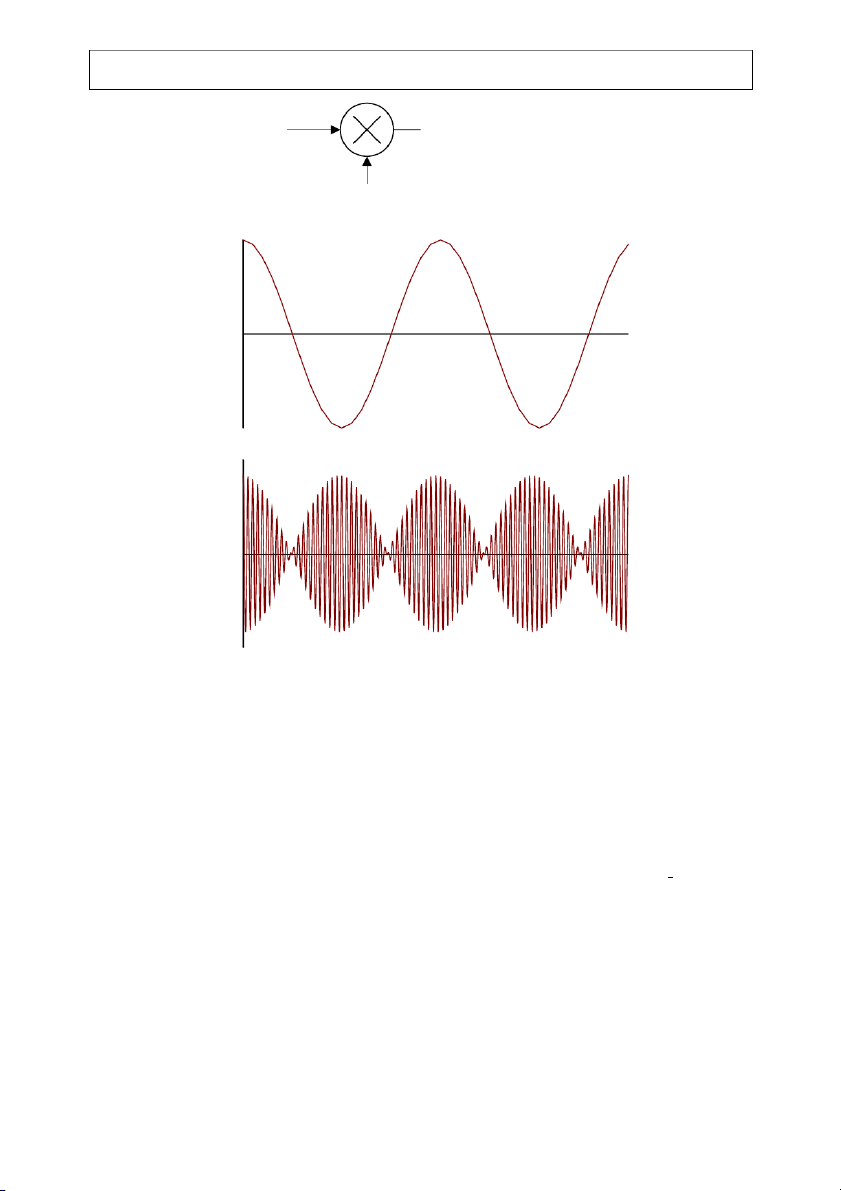
where Ac and φ0 are constants. For convenience, we will assume that φ0 = 0. Figures 2-1a
through 2-1c depict a block diagram of a DSB modulator, a sinusoidal message m and the DSB
time domain wave form xDSB(t), respectively. Note that every sign change in m(t) results in a
180° phase shift in the transmitted signal xDSB(t).
DSB is very popular when used to transmit digital data. In this application, m(t) is a
digital waveform that switches between +1 and -1 volts. Hence, m(t) switches the phase of the
transmitted carrier by π radians. For this reason, for a ±1 binary message, the modulation is
called phase shift keying.
The Fourier transform of xDSB is X ( jω) = F [x (t)] Ac DSB DSB = [M(jω+ j c ω ) + M( jω − jωc )], (2-3) 2 506CH2.DOC 2-1 EE426/506 Class Notes 07/12/06 John Stensby m(t) a) x (t) = A m(t)cosω t DSB c c A cosω t c c (t) m b) t (t) BS x D c) t
Figure 2-1: a) Block diagram of a DSB modulator. b) Sinusoidal
message. c) The resulting xDSB(t).
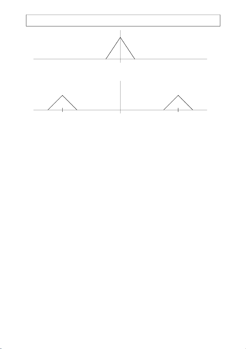
where M(jω) = F [m(t)] is the Fourier transform of the message. As shown by Figure 2-2,
XDSB(jω) is a scaled version of the message tranform that has been translated to ±ωc. As is usual,
we will assume that the message bandwidth is small compared to ωc, so xDSB(t) is a narrow band signal.
In general, XDSB(jω) contains a discrete carrier component (a spectral line) at ωc, an
upper sideband (the USB is the portion of Xc(jω) that lies above the carrier ωc) and a lower
sideband (the LSB is the portion of Xc(jω) which lies in the frequency range 0 < ω < ωc). If m(t)
has no DC component, then the carrier in Xc(jω) will be suppressed (any nonzero DC component 506CH2.DOC 2-2 EE426/506 Class Notes 07/12/06 John Stensby M(jω) -W W ω X (jω) DSB ½A M(jω + jω ) ½A M(jω − jω ) c c c c −ω ω ω c c
Figure 2-2: Spectrum M(jω) of message and spectrum XDSB(jω) of DSB signal.
of m(t) will lead to a nonzero carrier component). In many applications, in order to improve
efficiency, we seek to allocate no transmitter power to the carrier (the carrier conveys no
information about m(t) so it is desirable to allocated no power to the carrier). Finally, note that
the transmission bandwidth is twice the message bandwidth. DSB Demodulation
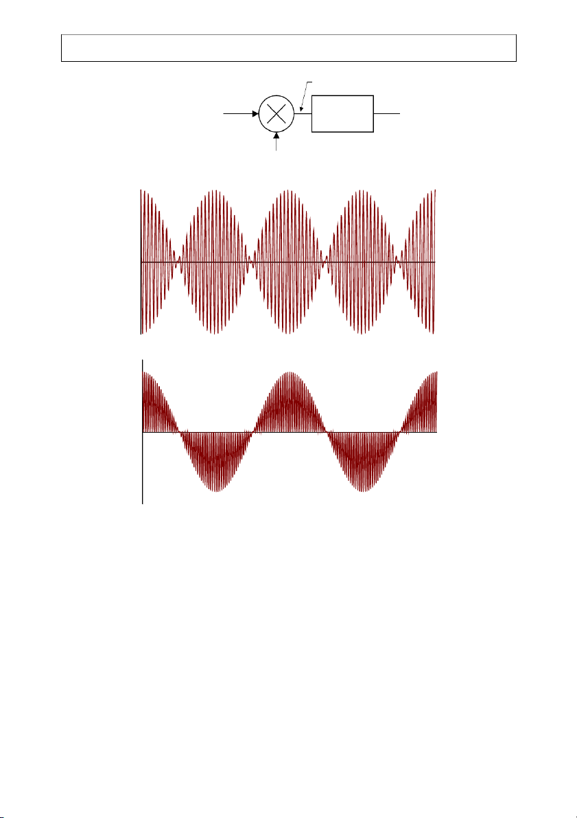
We assume that the received signal is a replica of the transmitted signal; that is xDSB(t) = Acm(t) cos c ω t . (2-4)
is received. As shown by Figure 2-3, demodulation involves multiplying xDSB by a phase
coherent replica of the carrier and then low-pass filtering the product. The output of the demodulator’s multiplier is d(t) = [Acm(t) cos c ω t]2 cos c ω t = c A m(t) + Acm(t)cos 2 c ω t . (2-5)
The low-pass filter (LPF) following the multiplier filters out all components centered at 2ωc. The output of the LPF is 506CH2.DOC 2-3 EE426/506 Class Notes 07/12/06 John Stensby x 2cosω t DSB c a) x (t) = A m(t)cosω t DSB c c A m(t) c LPF 2cosω t c x (t) DSB b) t x (t){2cosω t} DSB c c) t
Figure 2-3: a) DSB demodulator, b)xDSB and c) product of xDSB and coherent carrier. yd(t) = Acm(t) . (2-6)
A fundamental problem with DSB is the need for a phase coherent reference (i.e., the
2cosωct term) at the receiver. Complicating this problem is the fact that a carrier may not be 506CH2.DOC 2-4 EE426/506 Class Notes 07/12/06 John Stensby
transmitted, in many applications.
Let us analyze the effects of a phase error in the carrier used to demodulate xr. Assume
that our local reference is 2cos(ωct + θ(t)), where θ(t) is a phase error term. The multiplier’s output is d(t) = [Acm(t)cos c ω t]2cos( c ω t + ( θ t)) = c A m(t) cos ( θ t) + Acm(t)cos(2 c ω t + ( θ t)) , (2-7)
and the output of the LPF is, at best, yd(t) = Acm(t)cos ( θ t) (2-8)
(we assume this signal is within the pass band of the LPF). In yd, the time varying term cosθ(t)
could introduce serious distortion. On the other hand, depending on the application, it many not
matter much, if kept small. When m(t) is human voice, we usually can tolerate a small nonzero
frequency error dθ/dt and still make out what is being said. On the other extreme, when m(t) is
digital data, and a computer interprets the demodulated yd, small phase errors can be devastating.
There are ways to regenerate a phase coherent carrier at the receiver, even if one is not
transmitted. One commonly used method squares the received DSB signal to produce 2 2 2 2 1 2 2 1 2 2 xr (t) = Ac m (t)cos c
ω t = Ac m (t) + Ac m (t) cos 2 c ω t . (2-9) 2 2
If m(t) is a power signal, then m2(t) has a nonzero DC average. In this case, x 2 r has a discrete
spectral component at 2ωc which can be extracted by a narrow band filter centered at 2ωc. The
extracted 2ωc component is divided by two in frequency (by a D flip-flop, for example) to
generate a coherent reference at the receiver.
Figure 2-4 depicts a block diagram of a DSB demodulator that utilizes a squaring 506CH2.DOC 2-5 EE426/506 Class Notes 07/12/06 John Stensby Input m(t) sinω t ≈ -½cos2ω t Phase Locked Loop c c BPF x x2 BPF Loop ( )2 @ω @2ω Filter c c ≈ m(t) LPF ÷2 VCO 2sinω t 2sin2ω t c c
Figure 2-4: Block diagram of a squaring loop DSB demodulator. The VCO
output is divided by two in frequency to obtain a phase-coherent reference
for coherent demodulation of the input DSB signal.
operation. In this application, a phase lock loop (PLL) serves to recover the 2ωc component in x2
(the PLL “locks” onto the 2ω 2
c component in x ). That is, the PLL acts like a narrow band-pass
filter that extracts the 2ωc component from its input. Under proper operation (i.e., when the
closed loop phase error is small), the phase of the VCO output leads by π/2 radians the phase of
the PLL input. Hence, the VCO output is 2sinωct, a result that is divided by two in frequency to
produce a coherent reference for demodulating the DSB input. Since the demodulator relies on
the nonlinear operation x2, the demodulator is often called a squaring loop. Amplitude Modulation
Amplitude modulation was invented by Reginald A. Fessenden, a Canadian, who
successfully transmitted, for the first time, the sound of human voice. He first transmitted voice
between two 50-foot towers on Cobb Island located in the Potomac River, Washington D.C.,
December 23rd, 1900. Prior to AM, radio operators used crude spark gap transmitters to send only Morse code.
At the time, few people shared Fessenden's belief that broadcasting the human voice was
possible, much less practical. When Fessenden asked the opinion of the great Thomas Edison,
Edison replied, "Fezzie, what do you say are man's chances of jumping over the moon? I think
one is as likely as the other." Fortunately, Edison was wrong. 506CH2.DOC 2-6 EE426/506 Class Notes 07/12/06 John Stensby
It took six years for Fessenden to refine his invention but, on Christmas Eve 1906,
Fessenden made the first radio broadcast (of speech and music) in history from Brant Rock
Station, Massachusetts. Radio operators on ships in the Atlantic were shocked to hear a human
voice emitting from the equipment they used to receive Morse code. Many operators called their
Captains to the radio room, where they heard Fessenden make a short speech, play a record, and
give a rendition of "O Holy Night" on his violin.
Since the 1920’s, AM has been used in commercial broadcasting. Also, it is still used in
civil aviation and amateur radio. Most signal generators can be AM modulated by a built-in
modulator. Also, other types of test equipment can modulate/demodulate AM.
AM results when a DC bias A is added to message m(t) prior to the DSB modulation
process (in what follows, we assume that m(t) has a zero DC component). This results in the
transmission of a carrier component if bias A ≠ 0. The AM signal is defined as x
(t) = [A + m(t) ]A cos ω t = A′ [1 +a mn (t)]cos ω t AM c c c c , (2-10) = Ac′ cosωct + Ac′a mn (t)cosωct carrier component sideband component where min{ m(t)} m(t) Ac′ ≡ AAc, t n m (t) ≡ , a ≡ . (2-11) min{ m(t)} A t
mn(t) is message m(t) normalized so that the minimum value of mn(t) is -1. Parameter a, a ≥ 0, is
known as the modulation index. The quantity c A′ [1+ a n m (t ]
) is known as the envelope of AM
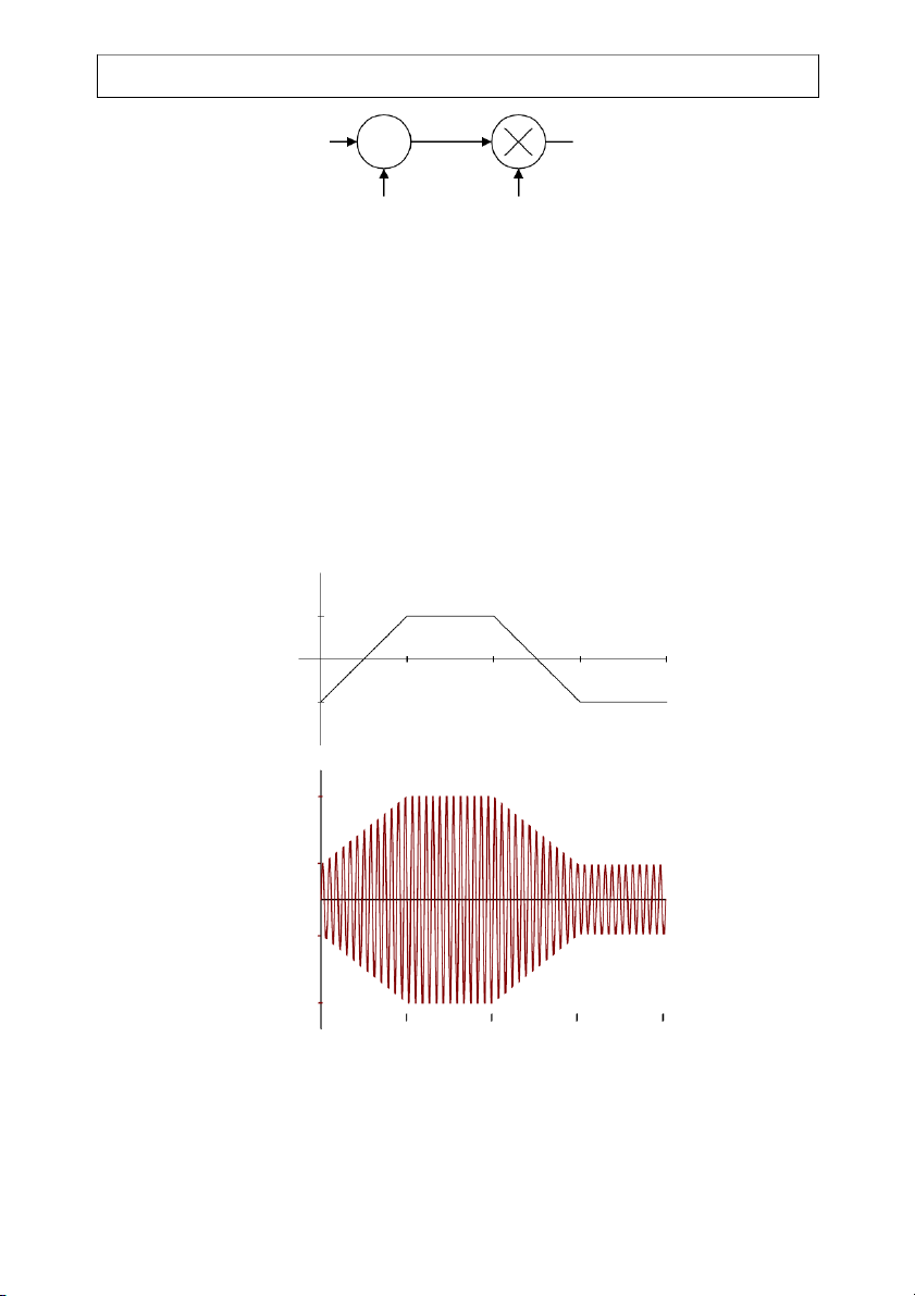
signal xc(t). For a ≤ 1, the envelope is never negative, and the message appears to “ride” on top 506CH2.DOC 2-7 EE426/506 Class Notes 07/12/06 John Stensby m(t) A+m(t) x (t) Σ AM A A cosω t c c
Figure 2-5: AM modulator
of the transmitted signal. For a > 1, the signal experiences a π-radian phase shift at each zero
crossing of the envelope (a fact of important significance as discussed below). See Figure 2-5
for a block diagram of an AM modulator and Figure 2-6 for an example of a message and AM modulated signal.
In the frequency domain, the spectrum of AM is m (t) n 1 T/4 T/2 3T/4 T -1 xAM A ′(1+a) c A ′(1-a) c t -A ′(1-a) c -A ′(1+a) c T/4 T/2 3T/4 T
Figure 2-6: Message mn and AM waveform xAM. 506CH2.DOC 2-8 EE426/506 Class Notes 07/12/06 John Stensby X ( ) ω = F x
(t) =F A′ cos ω t + A′ a m (t) cos ω t AM [ AM ] [ c c c n c ] (2-12) = [ ′ ′ π ( δ ω + ω ) + ( δ ω − ω )] c A a A c c c + [Mn(ω+ c ω ) +M n( ω − c ω )] 2 carrier spectrum sideband spectrum
Note the existence of discrete carrier spectral lines at ±ωc. Also, the translated message terms
Mn(ω±ωc) contain upper and lower sidebands (Mn(ω-ωc), for ω > ωc, is an upper side band while
Mn(ω-ωc), for 0 < ω < ωc, is a lower side band). Finally, note that the transmission bandwidth of
AM is twice the message bandwidth, just like DSB.
The transmitted signal power is divided between the carrier and information conveying
side bands. Power allocated to the carrier is (in the sense that it does not convey information)
wasted. This leads to the notion of efficiency. Efficiency of AM
The average transmitted power of the AM signal is 2 2 2 2 2 2 1 xc(t) = [A + m(t)] Ac cos c
ω t = [A + m(t)] Ac (1+ cos 2 c ω t) . (2-13) 2
If m(t) is slowly varying with respect to cos2ωct, this last equation leads to the approximation 2 1 2 ⎡ 2 2 ⎤ 1 2 ⎡ 2 2 ⎤ xc(t) ≈ Ac A + 2A m(t) + m(t) = Ac A + m(t) 2 ⎢⎣ ⎥⎦ 2 ⎢⎣ ⎥⎦ , (2-14) since m(t) = 0 by assumption.
Define efficiency as the percentage of total power that conveys information. More
precisely, efficiency is the percentage of total transmitted power that is in the sidebands. From
the last equation, we can write 2 m Efficiency = × (100%) . (2-15) 2 2 A + m 506CH2.DOC 2-9 EE426/506 Class Notes 07/12/06 John Stensby Since m(t) = aAmn(t) we have 2 2 a m n Efficiency = × (100%) . (2-16) 2 2 1+ a mn
For a ≤ 1 the maximum efficiency is 50% (for a square wave message with a = 1). If m(t) is a
sine wave, and a = 1, then efficiency = 33%. For most complex messages, such as voice, efficiency is under 10%.
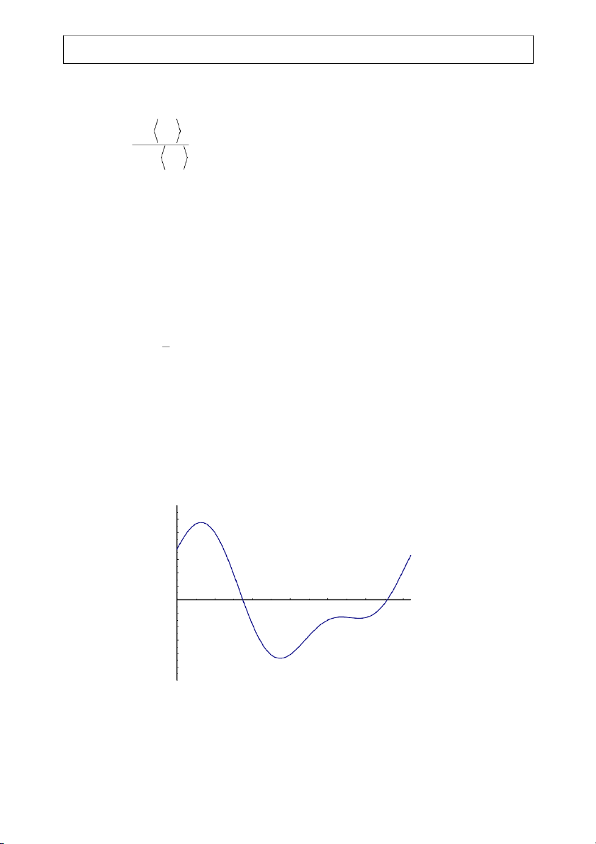
Example 2-1: Determine the efficiency and output xAM(t) for an AM modulator operating with
a modulation index of .5. The carrier power is 50 watts, and the message signal is m(t) 4 cos[ π = ωmt − ] + 2sin[2 m ω t] , (2-17) 9
a graph of which is depicted by Figure 2-7.
Solution: Observe the message signal shown in Fig. 2.7. The minimum value of m(t) is -4.364,
and the minimum falls at ωmt = 2π(.435). The normalized message signal is given by m(t) 6 5 4 3 2 1 0 ω t 0 1 2 3 4 5 6 m -1 -2 -3 -4 -5
Figure 2-7: One period of a two tone message. 506CH2.DOC 2-10 EE426/506 Class Notes 07/12/06 John Stensby 1 ⎡ π ⎤ π n m (t) = 4 cos[ m ω t − ]+ 2sin[2 m ω t] = .9166 cos[ m ω t − ]+ .45832 sin[2 m ω t] ⎣ 9 ⎦ . (2-18) 9 4.364
The mean-square value of mn(t) is 2 1 2 1 2 n
m (t) = (.9166) + (.4583) =.5251 (2-19) 2 2 Finally, the efficiency is .25(.5251) Efficiency = × (100%) = 11.60% (2-20) 1+ .25(.5251)
Since the carrier power is 50 watts, we have 1 2 (Ac′) = 50 (2-21) 2 which implies that
Ac′ =10 . Since sin(x) = cos(x - π/2), we can write ⎡ ⎤ x π π c (t) = 10 1 + .5 ⎣ (.9166cos( m ω t − ) + .4583cos(2 m ω t − )) cos c ω t 9 2 ⎦ . (2-22)
Transmitted Power in AM Signal
The transmitted AM signal is given by x (t) = A′ [1+ a m n(t ] ) cos ω t (2-23) AM c c 506CH2.DOC 2-11 EE426/506 Class Notes 07/12/06 John Stensby
The instantaneous transmitted power is 2 x
(t) . The average power in xA M is given by AM 2 2 2 2 1 (A′c ) ⎡ 2 2 ⎤ A P VG = x (t) = (A′ ) 1+ a m (t) (1+ cos 2ω t) = 1+ a m (t) AM c [ n ] c n 2 2 ⎢⎣ ⎥⎦ , (2-24)
watts. To obtain this result, we used the fact that message m(t) has an average value of zero.
Often, power is specified in terms of peak envelope power. The envelope Ac′[1 + amn(t)]
is slowly varying with respect to the RF carrier cosωct. Over every cycle of the RF carrier, the
envelope is approximately constant. The peak envelope power (PEP) is the instantaneous power
[xAM(t)]2 averaged over the RF cycle having the greatest amplitude. Hence, we can write 2 (A′ ) P = max [1 +a m (t)]2 c PEP n . (2-25) 2 t
For mn = cosωmt and a = 1, we get PAVG = 3A′2/4 and PPEP = 2A′2, so PPEP is about 2.7 times
PAVG. For a message consisting of a human voice, the PEP power might be two or three times (or more) the average power.
AM Coherent Demodulation
Amplitude modulation can be demodulated coherently, see Figure 2-8. The demodulate
output contains a constant DC term that is usually eliminated by a lack of DC response in the
audio stages that follow the demodulator. The coherent reference needed by the demodulator
can be supplied by phase locking a PLL onto the carrier component of xAM. The PLL acts like a
narrow-band filter that extracts the carrier component of the signal. Note that coherent x
(t) = A′ [1+ a mn(t)]cos ω t AM c c ′c A LPF [1 + a n m (t)] 2 cos ωt c
Figure 2-8: Coherent demodulation of AM. 506CH2.DOC 2-12 EE426/506 Class Notes 07/12/06 John Stensby + + x (t) C R v (t) ≈ m(t) AM out - -
Figure 2-9: A simple envelo pe detector.
demodulation can be used regardless of the modulation index a.
AM Demodulation - Envelope Detection
If modulation index a is equal to, or less than, unity (a ≤ 1), AM can be demodulated by a
very simple technique called envelope detection. On the other hand, if a > 1, envelope detection
will not work; the detector output audio will be highly distorted. The reason for this is simple.
For a > 1, the signal experiences a 180° phase change at each envelope sign change, and
envelope detectors are insensitive to signal phase. So, an envelope detector will not respond to
sign changes in the AM signal envelope, and distortion of the recovered audio results. A simple
envelope detector will only work if 0 ≤ a ≤ 1. Figure 2-9 depicts a schematic diagram of a simple envelope detector.
As long as envelope Ac′ [1+ a mn (t ]
) is non-negative, message m(t) appears to “ride” on
top of half-wave rectified xc(t). In this case, a close approximation of Ac′ [1+ a mn (t ] ) can be
obtained by smoothing the output of the diode with an RC circuit. The time constant of the RC
smoothing circuit is not extremely critical. However, as a general rule of thumb, best results can be obtained if 1 1 << RC << , (2-26) fc fB
where fc is the carrier frequency in Hz, and fB is the message bandwidth, in Hz.
The diode is assumed to have a small forward “on” resistance; the charging time constant
is extremely small (charging occurs when xAM > vout). Except for the drop across the diode,
output vout “follows” input xAM when the diode is conducting. When xAM < vout, the diode is not
conducting, and capacitor voltage vout discharges through the resistor. If the discharging time 506CH2.DOC 2-13 EE426/506 Class Notes 07/12/06 John Stensby
constant RC is too small, a severe “saw-tooth-like buzz”, at frequency fc, will be imposed on the
demodulated message. If RC is too large, the output will “float” on envelop peaks, and severe
distortion will occur. It is important to realize that, due to the nonlinear switching action of the
diode, the role of the RC circuit is to smooth the output and form a signal that follows closely the
modulation envelope. In this nonlinear circuit, do not think of the RC circuit as just a
conventional, single-pole low-pass filter.
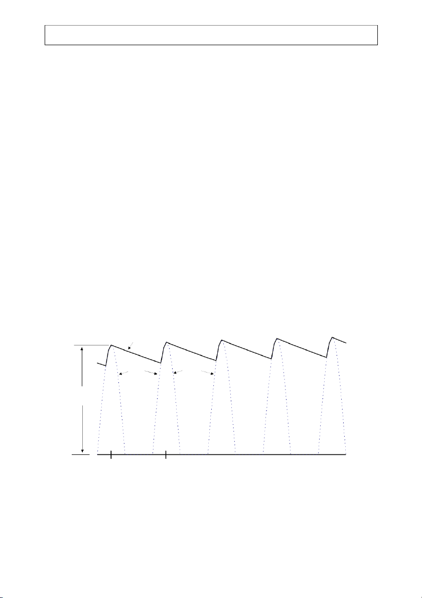
A relatively simple upper bound can be obtained on time constant RC for the case of a
sinusoidal message. As shown on Figure 2-10, assume that the capacitor discharges from the
carrier peak value E0 = c A′ [1+ a cos m ω 0
t ] at time t0. Note that t0 is associated with a peak in
the carrier, not the message or envelope (cosωmt0 can be any value between –1 and +1). For a
range of t between t0 and t0 + 1/fc, the capacitor is discharging, so the capacitor voltage is (t t0 ) / RC (t) 0e− − = c V E . (2-27)
The time interval between two successive carrier peaks is 1/fc = 2π/ωc. Since RC >> 1/ωc, the
quantity t/RC is small for time t between carrier peaks and vOUT x x AM AM E0 t t t + 1/f 0 0 c
Figure 2-10: Positive half of xAM shown as dotted-line graph. Output vOUT(t) depicted
as solid line graph. E0 is vOUT(t0), and the carrier frequency is fc. 506CH2.DOC 2-14 EE426/506 Class Notes 07/12/06 John Stensby ⎛ t − t ⎞ 0 (t) ≈ c V 0 E 1 − ⎜ ⎟ . (2-28) ⎝ RC ⎠
Suppose the signal peaks at time t0. If Vc(t) is to follow the envelope, then it is required that ⎛ ⎞ [ 1 1+ a cos ωmt0 ] 1 ⎜ −
⎟ ≤ 1+ a cos ωm(t 0 +1/ f c) . (2-29) ⎝ RC f c ⎠
Since ωm << ωc, we have (use the identity cos(α+β) = cosα cosβ - sinα sinβ and the fact that
cosβ ≈ 1 and sinβ ≈ β for small β )
1+ a cos ωm(t0 + 1/ fc) = 1+ a cos(ωmt0 + ωm / fc) ⎛ ⎞ ⎛ ⎞ ωm ωm = 1 + a cos( m ω t0)cos⎜ ⎟ − a sin( m ω t0)sin⎜ ⎟ (2-30) ⎝ fc ⎠ ⎝ fc ⎠ ⎛ ⎞ m ω ≈ 1 + a cos(ωmt0) − a ⎜ ⎟sin(ωmt0). ⎝ fc ⎠
Now, the last two equations combine to yield ⎛ ⎞ ⎛ ⎞ [ 1 ω 1+ a cos ωmt0 ] m ⎜ ⎟ ≥ a ⎜ ⎟sin(ωmt0) . (2-31) ⎝ RC fc ⎠ ⎝ fc ⎠ This result can be written as 1 a + cos m ω t0 ≥ a m ω sin ωmt0 (2-32) RC RC or 506CH2.DOC 2-15 EE426/506 Class Notes 07/12/06 John Stensby 2 ⎛ 1 ⎞ ⎛ ⎞ 2 1 − a ⎜ ω sin ω t − cosω t ⎟ = a ω + ⎜ ⎟ sin( 1 m m 0 m 0 m m ω 0 t − tan (1/ m ω RC )) ⎝ RC ⎠ ⎝ RC ⎠ . (2-33) 1 ≤ RC
Since ωmto is arbitrary, we must have 2 ⎛ ⎞ 2 1 1 a ωm + ⎜ ⎟ ≤ (2-34) ⎝ RC ⎠ RC and 2 1− a RC ≤ , (2-35) aωm
the desired upper bound on time constant RC.
Matlab Envelope Detector Simulation
The Matlab program listed in Figure 2-11 envelope detects the AM signal vin(t) =[1+ a sin(t)]sin(Wt) (2-36)
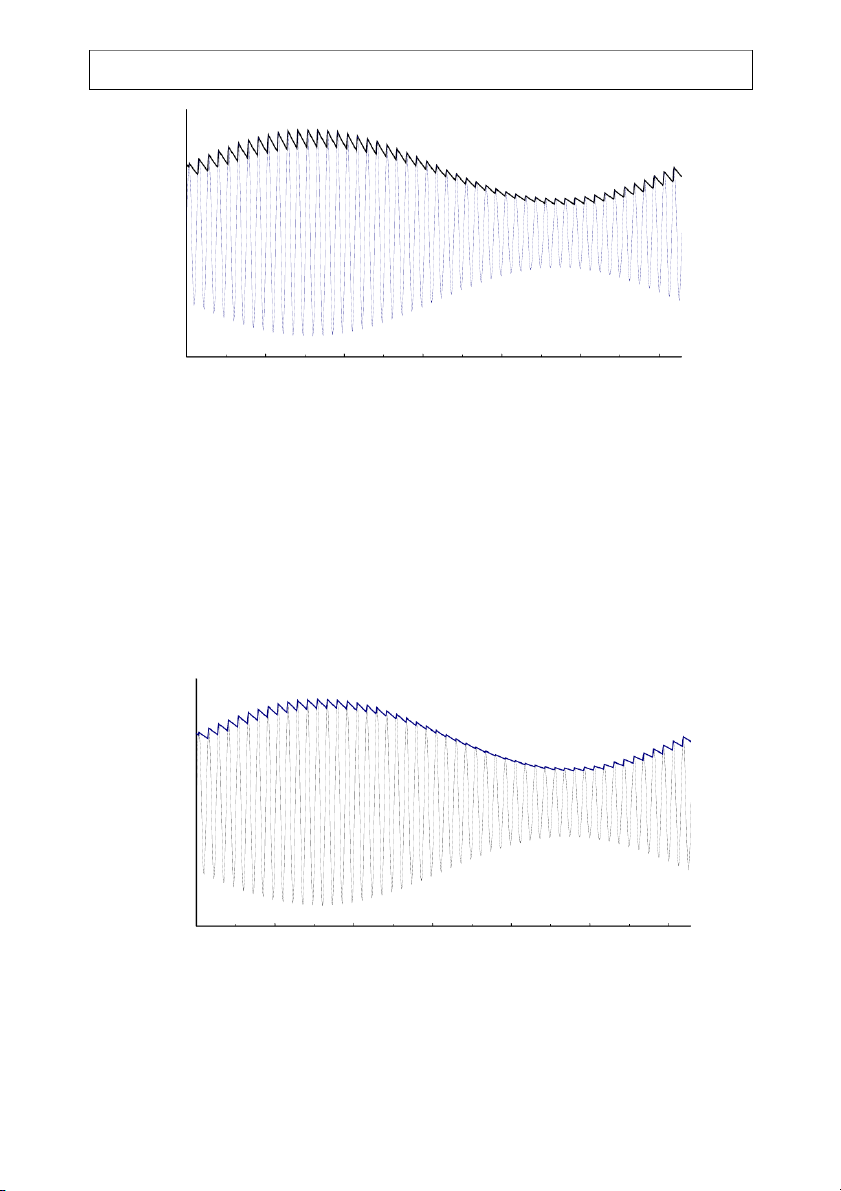
over the time period 0 ≤ t ≤ 2π. The results are depicted by Figs. 2-12 through 2-15; these
figures show the input vin as the “thin line” plot, and they show the envelope output as a “thick
line” plot (riding on top of vin).
To aid visualization, the values of W = 50 and Dt = 2π/1000 were used in all plots. The 506CH2.DOC 2-16 EE426/506 Class Notes 07/12/06 John Stensby %Envelope.m
%Envelope.m detects an AM waveform global RC, alpha, W, Dt; t = 0 : 2*pi/1000 : 2*pi;
%Allocate memory for input and output arrays Vin = zeros(1,1001); Vout = zeros(1,1001); %Define input array
Vin = ( 1 + alpha*sin(t) ).*sin(W*t);
%First point of output is the initial value of the envelope Vout(1) = 1;
%Compute output over all points for i = 2:1001 if Vin(i) > Vout(i-1); Vout(i) = Vin(i); else
Vout(i) = Vout(i-1)*exp(-Dt/RC); end end %Plot input then pause plot(t, Vin)
axis([0 2*pi -1-alpha 1+alpha]) pause %Hit any key to plot output plot(t, Vout) axis( [0 2*pi 0 1+alpha] )
Figure 2-11: Matlab program for simulation of an envelope detector.
carrier frequency is 50 times the message frequency (a ratio of 50 is smaller than what you
would normally encounter in practice). Also, a = .5 (50% modulation depth) was used for
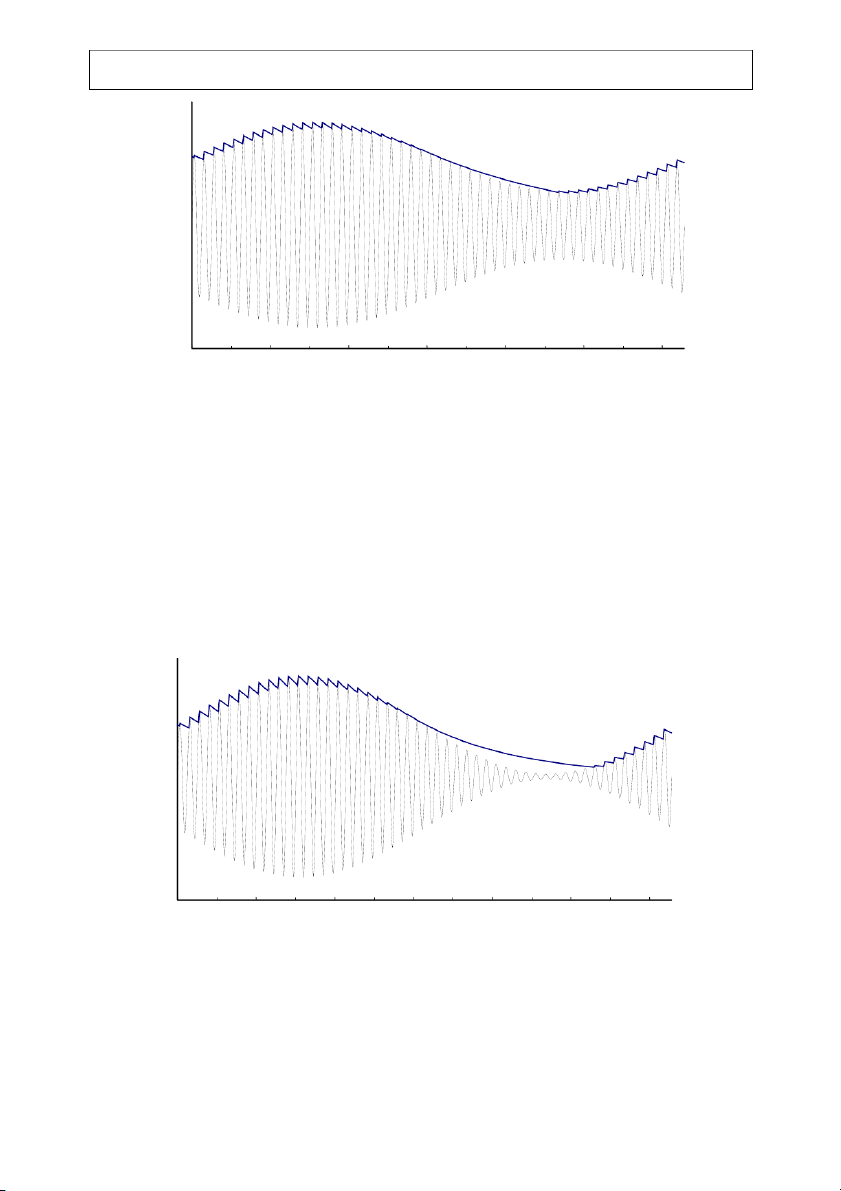
Figures 2-12 through 2-14. For Fig. 2-12, the RC time constant is 2π/10, a value that is a little
bit too small. For Fig. 2-13, the RC time constant is 2π/5, a value that is just about right. For
Fig. 2-14, the RC time constant is 2π/3, a value that is a bit too large (over part of the message
period, the envelope detector output “floats” above the true envelope - this causes harmonic 506CH2.DOC 2-17 EE426/506 Class Notes 07/12/06 John Stensby 1.5 1.0 0.5 0.0 -0.5 -1.0 -1.5 0 1 2 3 4 5 6 t
Figure 2-12: Input AM signal (thin line plot) and output of envelope detector (thick line plot).
The modulation index is ½. The RC time constant is 2π/10, a value that is a bit too small.
distortion in the demodulated output).
A “good” value of time constant RC depends on the modulation index a. As index a
approaches unity, you must use smaller values of RC to prevent demodulator output “floating”
with its associated harmonic distortion (some output distortion is unavoidable for near-unity
index values). For example, Figure 2-13 shows good results with RC = 2π/5 and a = ½.
However, significant distortion occurs if the same value of RC is used with a = .95, as can be
seen from examining Figure 2-15. 1.5 1.0 0.5 0.0 -0.5 -1.0 -1.5 0 1 2 3 4 5 6 t
Figure 2-13: Input AM signal (thin line plot) and output of envelope detector (thick line plot).
The modulation index is ½. The RC time constant is 2π/5, a value that is just about right. 506CH2.DOC 2-18 EE426/506 Class Notes 07/12/06 John Stensby 1.5 1.0 0.5 0.0 -0.5 -1.0 -1.5 0 1 2 3 4 5 6 t
Figure 2-14: Input AM signal (thin line plot) and output of envelope detector (thick line
plot). The modulation index is ½. The RC time constant is 2π/3, a value that is a bit too
large (the detector output floats” above the true envelope over part of the modulation period). Square-Law Detector
An amplitude modulated signal can be demodulated by a square law detector, if the
modulation index is sufficiently small. As depicted by Figure 2-16, a square law detector forms
its output vo by low-pass filtering the square of the input vin. If vin = ′c A [1+ a n m (t)]cos c ω t we get 2 1 0 -1 -2 0 1 2 3 4 5 6 t
Figure 2-15: Input AM signal (thin line plot) and output of envelope detector (thick line plot).
A value of modulation index a = .95 was used to obtain this plot. The RC time constant is
2π/5, a value that is too large (for a = .95) as is evident by the significant amount of detector output “floating”. 506CH2.DOC 2-19 EE426/506 Class Notes 07/12/06 John Stensby 2 v c A′ ⎛ 2 2⎞ in = Ac′[1+ a mn]cos c ω t 0 v = 1 ⎜ + 2a n m + a n m ⎟ ⎝ ⎠ ( )2 LPF 2
Figure 2-16: A square-law detector. (A′ [1 +a mn(t) ]cos ω t )2 2 =A ′ ( 2 2 1 +2a m (t) +a m (t) ) 1 c c c n n (1 +cos 2 c ω t) . (2-37) 2
The low-pass filter removes the 2ωc component to produce the output 2 A c′ . (2-38) o v ( t ) = ( 2 2
1 + 2 a m n ( t ) + a m n ( t ) 2 ) The second-order term 2
mn(t) introduces second-order harmonic distortion that can be severe if
modulation index a is not small. On the other hand, if a << 1 and a blocking capacitor is used to
remove the DC component, this last result can be approximated by 2
vo(t) ≈ Ac′ a mn (t) . (2-39)
The nonlinear squaring operation can be implemented by a diode that is forward biased
into the “knee” of its i-v characteristic, see Fig. 2-17. The DC voltage source (the battery on the
figure) serves to forward bias the diode into its “square law” region. It is important to remember
that the input signal is small compared to the DC bias so that the diode always is forward biased
(unlike the envelope detector). Unlike its use in the envelope detector, the RC network serves as AM Input output
Figure 2-17: Approximation to Square Law Detector 506CH2.DOC 2-20
