
Preview text:
lOMoAR cPSD| 58707906
Problems Chapter 9 – Sequential Circuits
1. Construct a JK flip-flop using a D flip-flop, a two-to-one-line multiplexer, and an inverter.
2. Show that the characteristic equation for the complement output of a JK flip-flop is
̅𝑸̅̅̅𝒕+𝟏̅̅ = 𝑱̅̅𝑸̅̅̅ + 𝑲𝑸̅̅
3. Explain the differences among a truth table, a state table, a characteristic table, and an
excitation table. Also, explain the difference among a Boolean equation, a state
equation, a characteristic equation, and a flip-flop input equation.
4. A sequential circuit with two D flip-flops A and B, two inputs, x and y; and one output z
is specified by the following next-state and output equations
𝑨𝒕+𝟏 = 𝒙𝒚̅̅ + 𝒙𝑩
𝑩𝒕+𝟏 = 𝒙𝑨 + 𝒙𝑩̅ 𝒛 = 𝑨
(a) Draw the logic diagram of the circuit.
(b) List the state table for the sequential circuit. (c) Draw the corresponding state diagram.
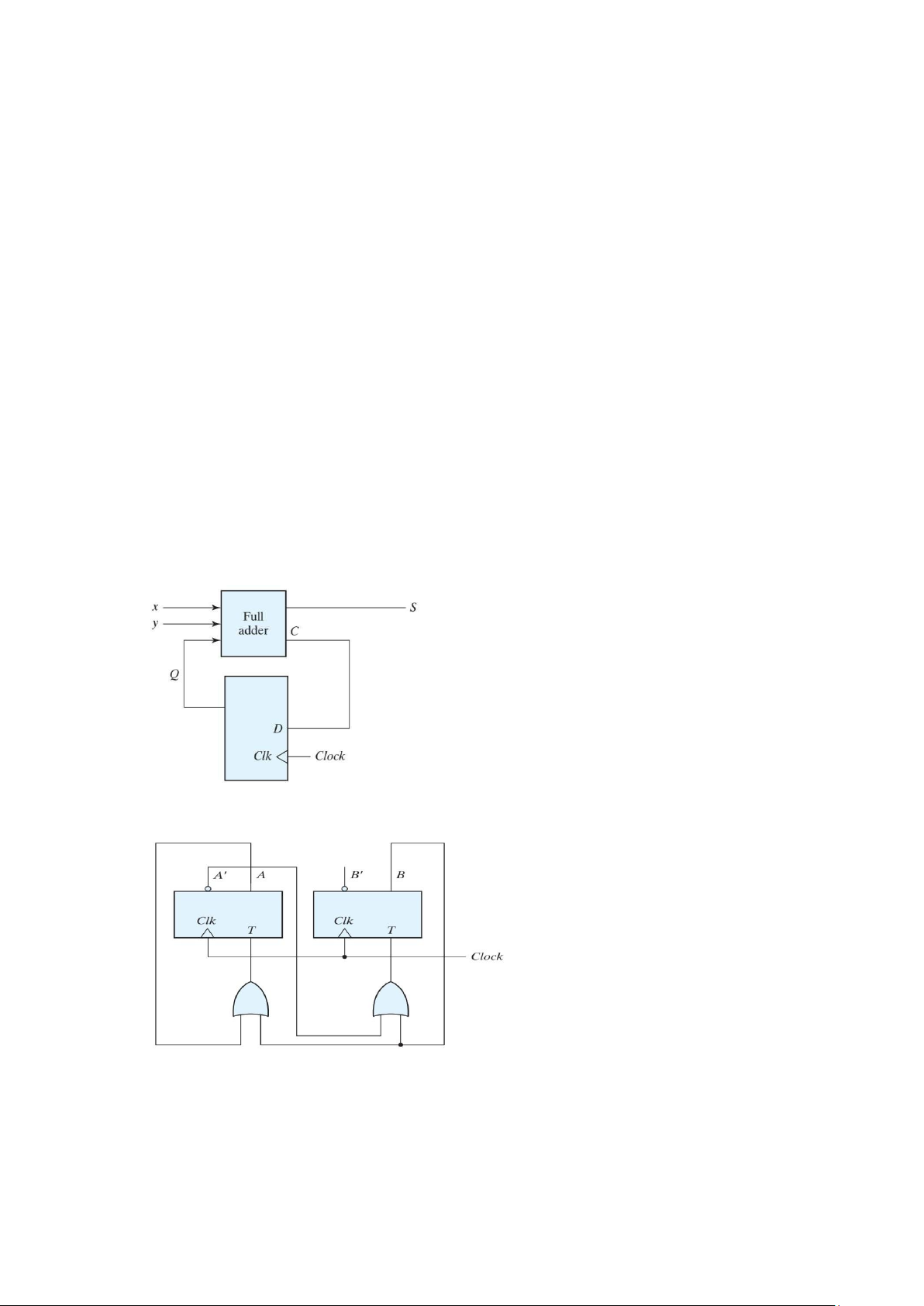
5. A sequential circuit has one flip-flop Q, two inputs x and y, and one output S. It consists
of a full-adder circuit connected to a D flip-flop, as shown in Fig. P5.7 . Derive the state
table and state diagram of the sequential circuit
6. Derive the state table and the state diagram of the sequential circuit shown in Fig. P5.8.
Explain the function that the circuit performs
7. A sequential circuit has two JK flip-flops A and B and one input x. The circuit is
described by the following flip-flop input equations: JA = x KA = B JB = x KB = A
(a) Derive the state equations A(t + 1) and B(t + 1) by substituting the input equations for the J and K variables. lOMoAR cPSD| 58707906
(b) Draw the state diagram of the circuit
8. A sequential circuit has two JK flip-flops A and B, two inputs x and y, and one output z.
The flip-flop input equations and circuit output equation are
𝑱̅𝑨 = 𝑩𝒙 + 𝑩̅𝒚̅̅
𝑲𝑨 = 𝑩̅𝒙𝒚̅̅
𝑱̅𝑩 = 𝑨̅𝒙
𝑲𝑩 = 𝑨 + 𝒙𝒚̅̅
𝒛 = 𝑨𝒙̅ 𝒚̅̅ + 𝑩𝒙̅ 𝒚̅̅
(a) Draw the logic diagram of the circuit. (b) Tabulate the state table.
(c) Derive the state equations for A and B.
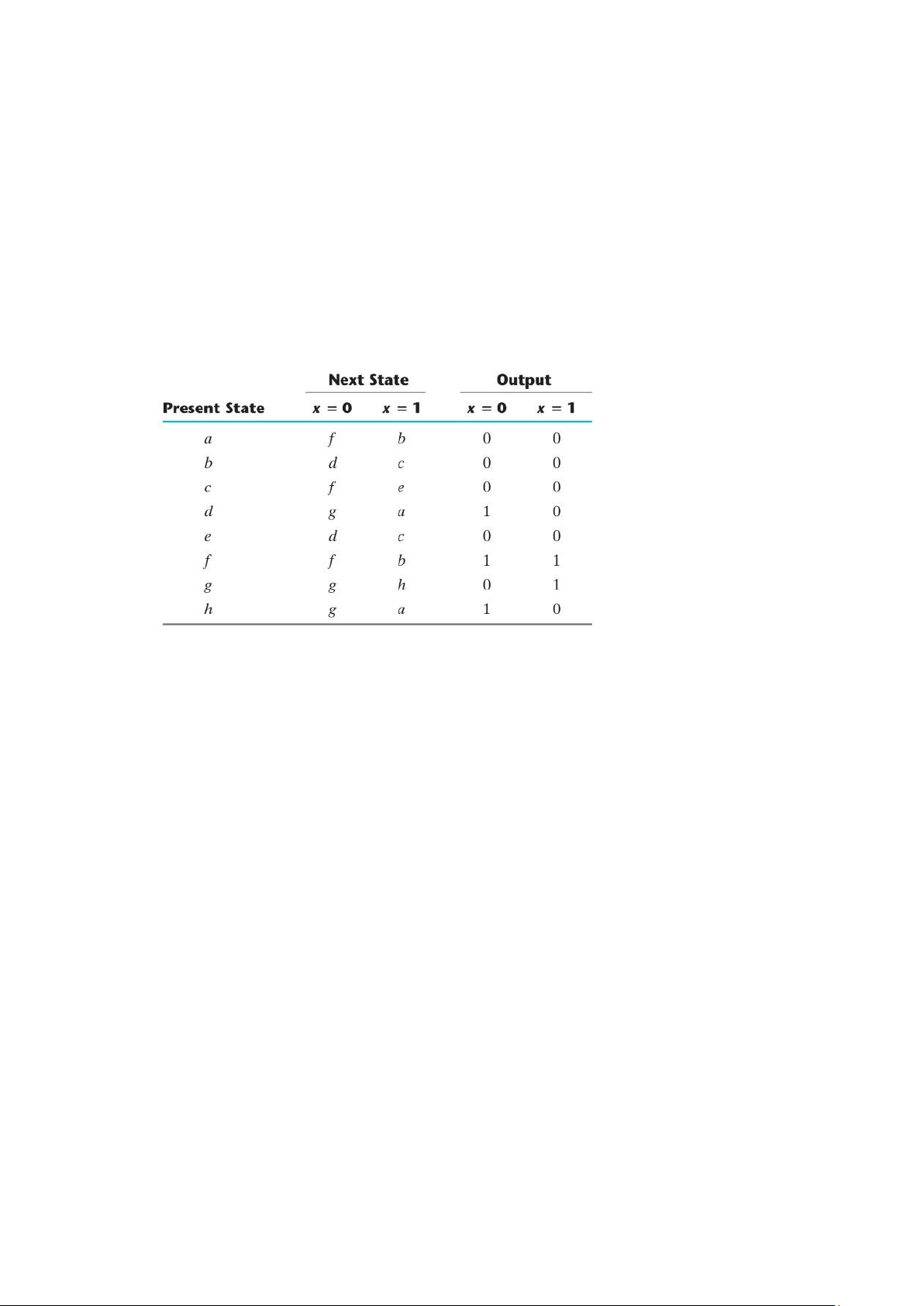
9. For the following state table
(a) Draw the corresponding state diagram.
(b) Tabulate the reduced state table.
(c) Draw the state diagram corresponding to the reduced state table
Starting from state a, and the input sequence 01110010011, determine the output sequence for
(a) The state table of the previous problem.
(b) The reduced state table. Show that the same output sequence is obtained for both
10. List a state table for the JK flip-flop using Q as the present and next state and J and K as
inputs. Design the sequential circuit specified by the state table
11. Design a one-input, one-output serial 2’s complementer. The circuit accepts a string of
bits from the input and generates the 2’s complement at the output. The circuit can be
reset asynchronously to start and end the operation
12. Design a sequential circuit with two JK flip-flops A and B and two inputs E and F. If E = 0,
the circuit remains in the same state regardless of the value of F. When E = 1 and F = 1,
the circuit goes through the state transitions from 00 to 01, to 10, to 11, back to 00, and
repeats. When E = 1 and F = 0, the circuit goes through the state transitions from 00 to
11, to 10, to 01, back to 00, and repeats
13. A sequential circuit has three flip-flops A, B, C; one input x_in; and one output y_out.
The state diagram is shown in Fig. P5.19 . The circuit is to be designed by treating the
unused states as don’t-care conditions. Analyze the circuit obtained from the design to
determine the effect of the unused states. (a) Use D flip-flops in the design. lOMoAR cPSD| 58707906
(b) Use JK flip-flops in the design
14. What is the difference between serial and parallel transfer? Explain how to convert
serial data to parallel and parallel data to serial. What type of register is needed?
15. The contents of a four-bit register is initially 0110. The register is shifted six times to the
right with the serial input being 1011100. What is the content of the register after each shift?
16. Design a four-bit shift register with parallel load using D flip-flops. There are two control
inputs: shift and load. When shift = 1, the content of the register is shifted by one
position. New data are transferred into the register when load = 1 and shift = 0. If both
control inputs are equal to 0, the content of the register does not change
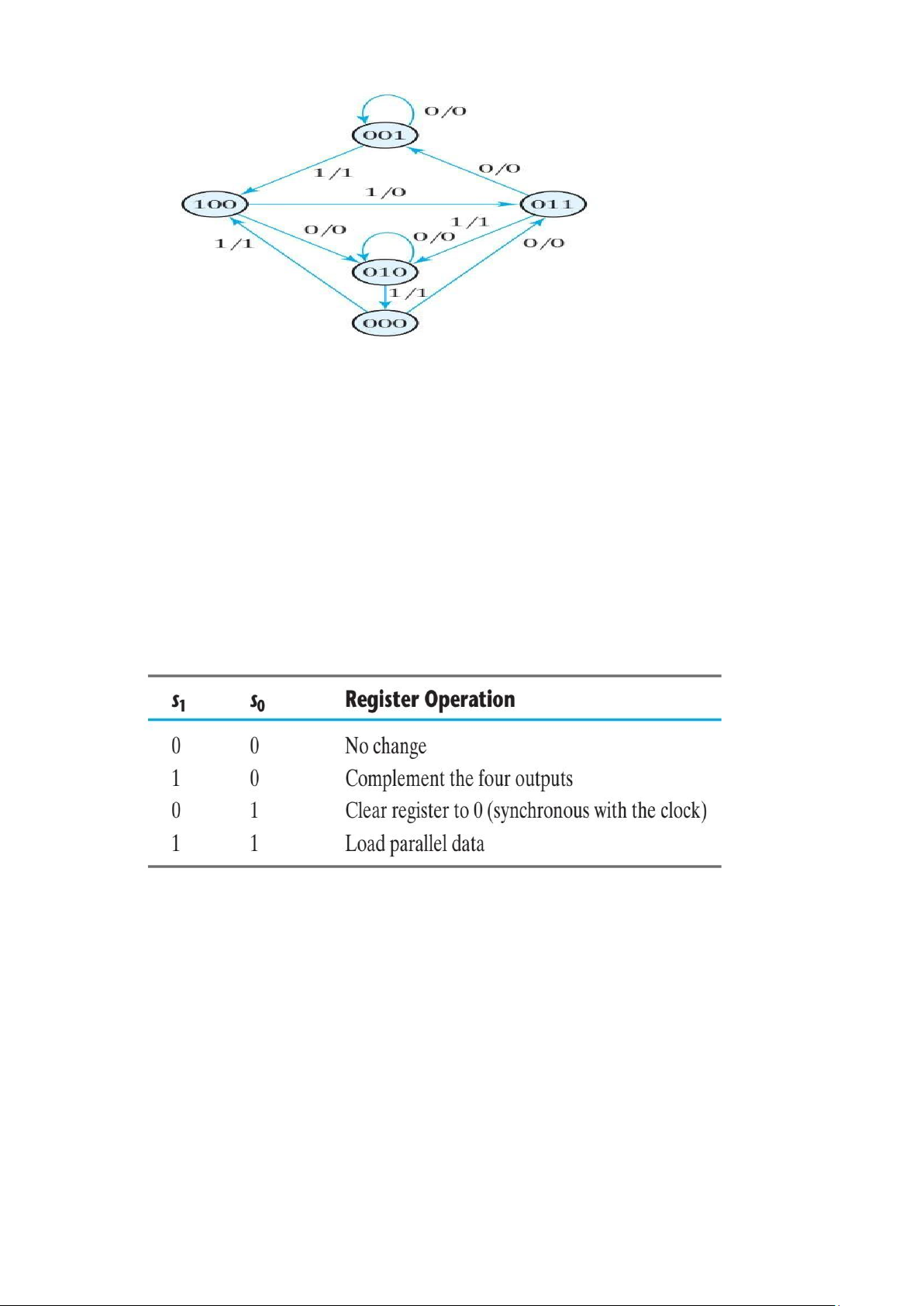
17. Draw the logic diagram of a four-bit register with four D flip-flops and four 4 × 1
multiplexers with mode selection inputs s1 and s0. The register operates according to
the following function table.
18. A binary ripple counter uses flip-flops that trigger on the positive-edge of the clock.
What will be the count if
(a) the normal outputs of the flip-flops are connected to the clock and
(b) the complement outputs of the flip-flops are connected to the clock?
19. Draw the logic diagram of a four-bit binary ripple countdown counter using (a) flip-flops
that trigger on the positive-edge of the clock and (b) flip-flops that trigger on the
negative-edge of the clock.
20. Design a four-bit binary synchronous counter with D flip-flop
21. Design a counter with T flip-flops that goes through the following binary repeated
sequence: 0, 1, 3, 7, 6, 4. Show that when binary states 010 and 101 are considered as
don’t care conditions, the counter may not operate properly. Find a way to correct the design
22. Using JK flip-flops, lOMoAR cPSD| 58707906
(a) Design a counter with the following repeated binary sequence: 0, 1, 2, 3, 4, 5, 6.
(b) Draw the logic diagram of the counter
