Pulse Oximeter IC Overview and Applications Guide | Iot và ứng dụng | Học viện Công nghệ Bưu chính Viễn thông
General Description The MAX30100 is an integrated pulse oximetry and heart- rate monitor sensor solution. It combines two LEDs, a photodetector, optimized optics, and low-noise analog signal processing to detect pulse oximetry and heart-rate signals. The MAX30100 operates from 1.8V and 3.3V power sup- plies and can be powered down through software with negligible standby current, permitting the power supply to remain connected at all times. Tài liệu được sưu tầm và soạn thảo dưới dạng file PDF để gửi tới các bạn cùng tham khảo, ôn tập đầy đủ kiến thức, chuẩn bị cho các buổi học thật tốt. Mời bạn đọc đón xem!
Môn: IoT và ứng dụng 143 tài liệu
Trường: Học viện Công Nghệ Bưu Chính Viễn Thông 1.8 K tài liệu
Tác giả:


Preview text:
EVALUATION KIT AVAILABLE MAX30100
Pulse Oximeter and Heart-Rate Sensor IC for Wearable Health General Description Benefits and Features
The MAX30100 is an integrated pulse oximetry and heart-
● Complete Pulse Oximeter and Heart-Rate Sensor
rate monitor sensor solution. It combines two LEDs, a Solution Simplifies Design
photodetector, optimized optics, and low-noise analog
• Integrated LEDs, Photo Sensor, and
signal processing to detect pulse oximetry and heart-rate
High-Performance Analog Front -End signals.
• Tiny 5.6mm x 2.8mm x 1.2mm 14-Pin Optically
The MAX30100 operates from 1.8V and 3.3V power sup- Enhanced System-in-Package
plies and can be powered down through software with
● Ultra-Low-Power Operation Increases Battery Life for
negligible standby current, permitting the power supply to Wearable Devices remain connected at all times.
• Programmable Sample Rate and LED Current for Power Savings Applications
• Ultra-Low Shutdown Current (0.7µA, typ) ● Wearable Devices
● Advanced Functionality Improves Measurement ● Fitness Assistant Devices Performance ● Medical Monitoring Devices
• High SNR Provides Robust Motion Artifact Resil- ience
• Integrated Ambient Light Cancellation
• High Sample Rate Capability
• Fast Data Output Capability
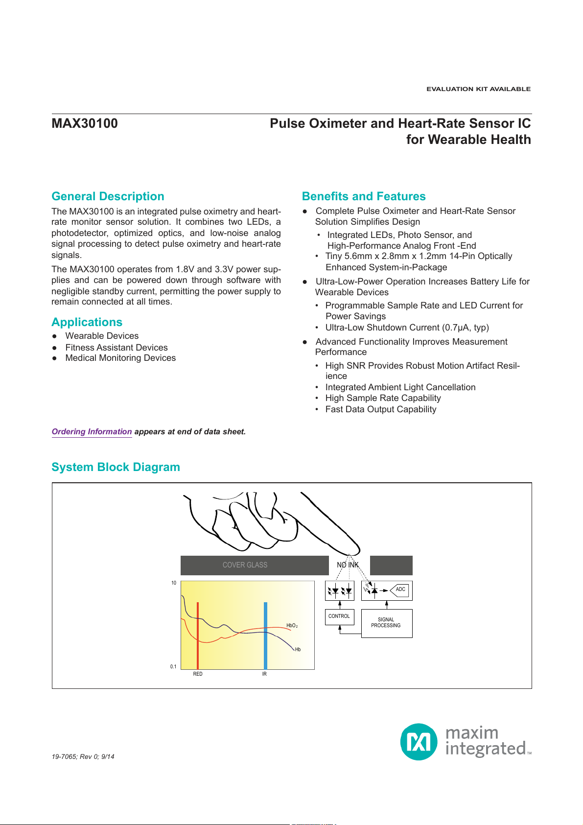
Ordering Information appears at end of data sheet. System Block Diagram COVER GLASS NO INK 10 ADC CONTROL SIGNAL HbO 2 PROCESSING Hb 0.1 RED IR 19-7065; Rev 0; 9/14 MAX30100
Pulse Oximeter and Heart-Rate Sensor IC for Wearable Health Absolute Maximum Ratings V
......................................................... DD to GND -0.3V to +2.2V
Continuous Power Dissipation (T = +70°C) A
GND to PGND ......................................................-0.3V to +0.3V
OESIP (derate 5.8mW/°C above +70°C) ....................464mW
x_DRV, x_LED+ to PGND ....................................-0.3V to +6.0V
Operating Temperature Range ........................... -40°C to +85°C
All Other Pins to GND ..........................................-0.3V to +6.0V
Soldering Temperature (reflow) ....................................... +260°C
Output Short-Circuit Current Duration .......................Continuous
Storage Temperature Range ............................ -40°C to +105°C
Continuous Input Current into Any Terminal ....................±20mA
Package Thermal Characteristics (Note 1) OESIP
Junction-to-AmbientThermalResistance(θJA) ........150°C/W
Junction-to-CaseThermalResistance(θJC) .............170°C/W
Note 1: Package thermal resistances were obtained using the method described in JEDEC specification JESD51-7, using a four-layer
board. For detailed information on package thermal considerations, refer to www.maximintegrated.com/thermal-tutorial. Electrical Characteristics (VDD = 1.8V, V = V
= 3.3V, T = +25 C, min/max are from T = -40 C to +85 C, unless otherwise noted.) (Note 2) IR_LED+ R_LED+ A ° A ° ° PARAMETER SYMBOL CONDITIONS MIN TYP MAX UNITS POWER SUPPLY Power-Supply Voltage V
Guaranteed by RED and IR count tolerance 1.7 1.8 2.0 V DD LED Supply Voltage V (R_LED+ or IR_LED+ to PGND) LED+
Guaranteed by PSRR of LED Driver 3.1 3.3 5.0 V SpO2 and heart rate modes, 600 1200 PW = 200µs, 50sps Supply Current IDD µA Heart rate only mode, 600 1200 PW = 200µs, 50sps Supply Current in Shutdown I = +25°C, MODE = 0x80 0.7 10 µA SHDN TA SENSOR CHARACTERISTICS ADC Resolution 14 bits Propriety ATE setup Red ADC Count RED RED_PA = 0x05, LED_PW = 0x00, 23,000 26,000 29,000 Counts (Note 3) C SPO2_SR = 0x07, T = +25°C A Propriety ATE setup IR ADC Count IR IR_PA = 0x09, LED_PW = 0x00, 23,000 26,000 29,000 Counts (Note 3) C SPO2_SR = 0x07, T = +25°C A RED_PA = IR_PA = 0x00, Dark Current Count DCC 0 3 Counts LED_PW = 0x03, SPO2_SR = 0x01 Number of ADC counts with
fingeronsensorunderdirect RED LED 0 DC Ambient Light Rejection ALR sunlight (100K lux) Counts (Note 4) LED_PW = 0x03, IR LED 0 SPO2_SR = 0x01 www.maximintegrated.com Maxim Integrated │ 2 MAX30100
Pulse Oximeter and Heart-Rate Sensor IC for Wearable Health
Electrical Characteristics (continued) (VDD = 1.8V, V = V
= 3.3V, T = +25 C, min/max are from T = -40 C to +85 C, unless otherwise noted.) (Note 2) IR_LED+ R_LED+ A ° A ° ° PARAMETER SYMBOL CONDITIONS MIN TYP MAX UNITS Propriety ATE setup 1.7V < VDD < 2.0V, 0.25 2 % IR ADC Count—PSRR (V
LED_PW = 0x03, SPO2_SR = 0x01, DD) PSRRVDD
IR_PA = 0x09, IR_PA = 0x05, T = +25°C A
Frequency = DC to 100kHz, 100mVP-P 10 LSB Propriety ATE setup 3.1V < X_LED+ < 5V, RED/IR ADC Count—PSRR 0.05 2 % PSRR
LED_PW = 0x03, SPO2_SR = 0x01, (X_LED+) LED
IR_PA = 0x09, IR_PA = 0x05, T = +25°C A
Frequency = DC to 100kHz, 100mVP-P 10 LSB LED_PW = 0x00 200 µs ADC Integration Time INT LED_PW = 0x03 1600 µs
IR LED CHARACTERISTICS (Note 4) LED Peak Wavelength λP ILED = 20mA, TA = +25°C 870 880 900 nm Full Width at Half Max Δλ ILED = 20mA, TA = +25°C 30 nm Forward Voltage VF ILED = 20mA, TA = +25°C 1.4 V Radiant Power PO ILED = 20mA, TA = +25°C 6.5 mW
RED LED CHARACTERISTICS (Note 4) LED Peak Wavelength λP ILED = 20mA, TA = +25°C 650 660 670 nm Full Width at Half Max Δλ ILED = 20mA, TA = +25°C 20 nm Forward Voltage VF ILED = 20mA, TA = +25°C 2.1 V Radiant Power PO ILED = 20mA, TA = +25°C 9.8 mW TEMPERATURE SENSOR Temperature ADC Acquisition T Time T TA = +25°C 29 ms Temperature Sensor Accuracy TA TA = +25°C ±1 °C Temperature Sensor Minimum T Range MIN -40 °C Temperature Sensor Maximum T Range MAX 85 °C www.maximintegrated.com Maxim Integrated │ 3 MAX30100
Pulse Oximeter and Heart-Rate Sensor IC for Wearable Health
Electrical Characteristics (continued) (VDD = 1.8V, V = V
= 3.3V, T = +25 C, min/max are from T = -40 C to +85 C, unless otherwise noted.) (Note 2) IR_LED+ R_LED+ A ° A ° ° PARAMETER SYMBOL CONDITIONS MIN TYP MAX UNITS
DIGITAL CHARACTERISTICS (SDA, SDA, INT) Output Low Voltage SDA, INT VOL ISINK = 6mA 0.4 V I2C Input Voltage Low VIL_I2C SDA, SCL 0.4 V I2C Input Voltage High VIH_I2C SDA, SCL 1.4 V Input Hysteresis VHYS SDA, SCL 200 mV Input Capacitance CIN SDA, SCL 10 pF VIN = 0V, T A = +25°C 0.01 1 µA (SDA, SCL, INT) Input Leakage Current IIN VIN = 5.5V, TA = +25°C 0.01 1 µA (SDA, SCL, INT)
I2C TIMING CHARACTERISTICS (SDA, SDA, INT) I2C Write Address AE Hex I2C Read Address AF Hex Serial Clock Frequency fSCL 0 400 kHz Bus Free Time Between STOP t and START Conditions BUF 1.3 µs Hold Time (Repeated) START t Condition HD,START 0.6 µs SCL Pulse-Width Low tLOW 1.3 µs SCL Pulse-Width High tHIGH 0.6 µs
Setup Time for a Repeated START t Condition SU,START 0.6 µs Data Hold Time tHD,DAT 0 900 ns Data Setup Time tSU,DAT 100 ns Setup Time for STOP Condition tSU,STOP 0.6 µs
Pulse Width of Suppressed Spike tSP 0 50 ns Bus Capacitance CB 400 pF SDA and SCL Receiving Rise t Time R 20 + 0.1CB 300 ns
SDA and SCL Receiving Fall Time tRF 20 + 0.1CB 300 ns SDA Transmitting Fall Time tTF 20 + 0.1CB 300 ns
Note 2: All devices are 100% production tested at T = +25°C. Specifications over temperature limits are guaranteed by Maxim A
Integrated’s bench or proprietary automated test equipment (ATE) characterization.
Note 3: Specifications are guaranteed by Maxim Integrated’s bench characterization and by 100% production test using proprietary ATE setup and conditions.
Note 4: For design guidance only. Not production tested. www.maximintegrated.com Maxim Integrated │ 4 MAX30100
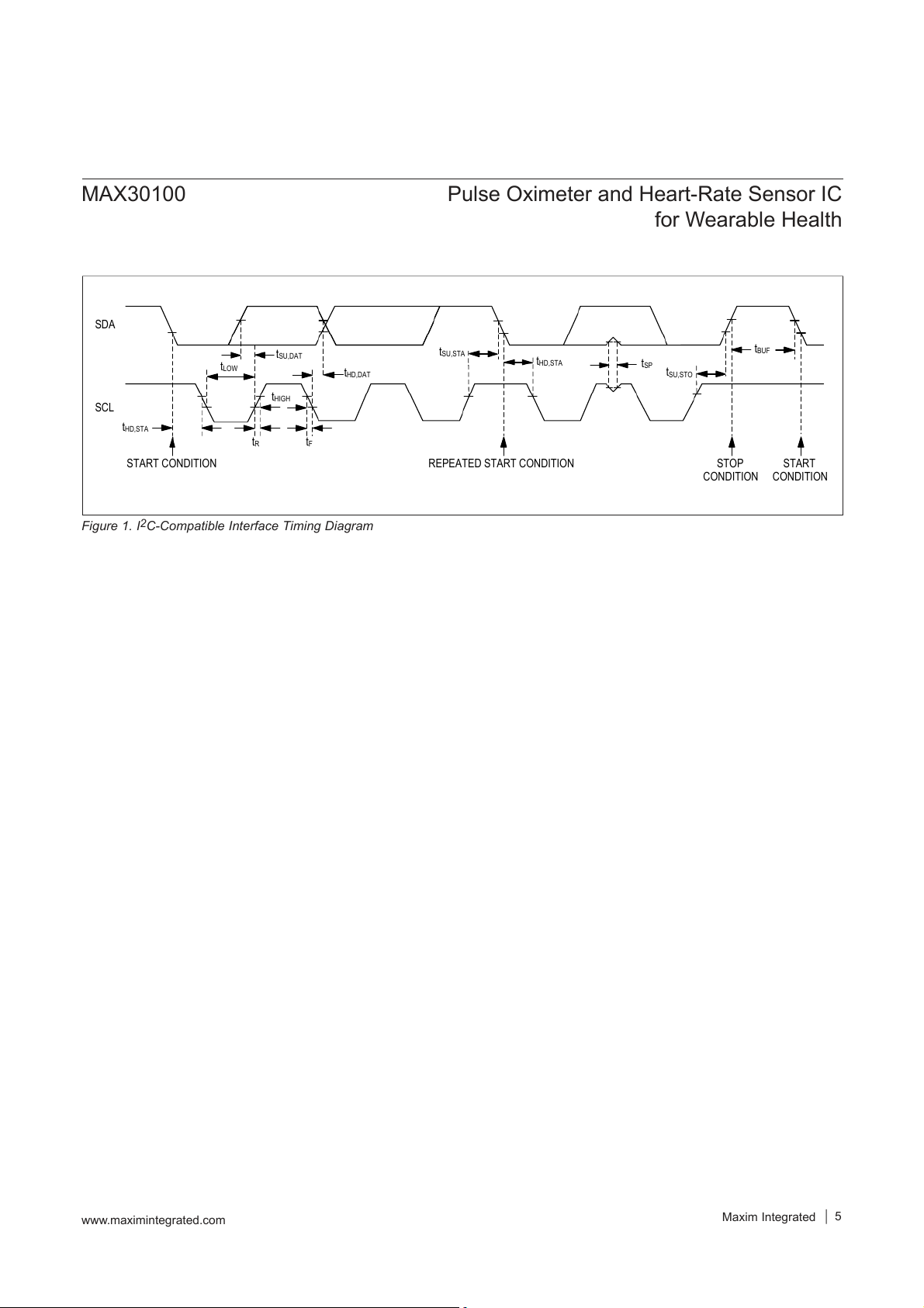
Pulse Oximeter and Heart-Rate Sensor IC for Wearable Health SDA t t t BUF SU,DAT SU,STA t tHD,STA t LOW SP tHD,DAT tSU,STO tHIGH SCL tHD,STA tR tF START CONDITION REPEATED START CONDITION STOP START CONDITION CONDITION
Figure 1. I2C-Compatible Interface Timing Diagram www.maximintegrated.com Maxim Integrated │ 5 MAX30100
Pulse Oximeter and Heart-Rate Sensor IC for Wearable Health
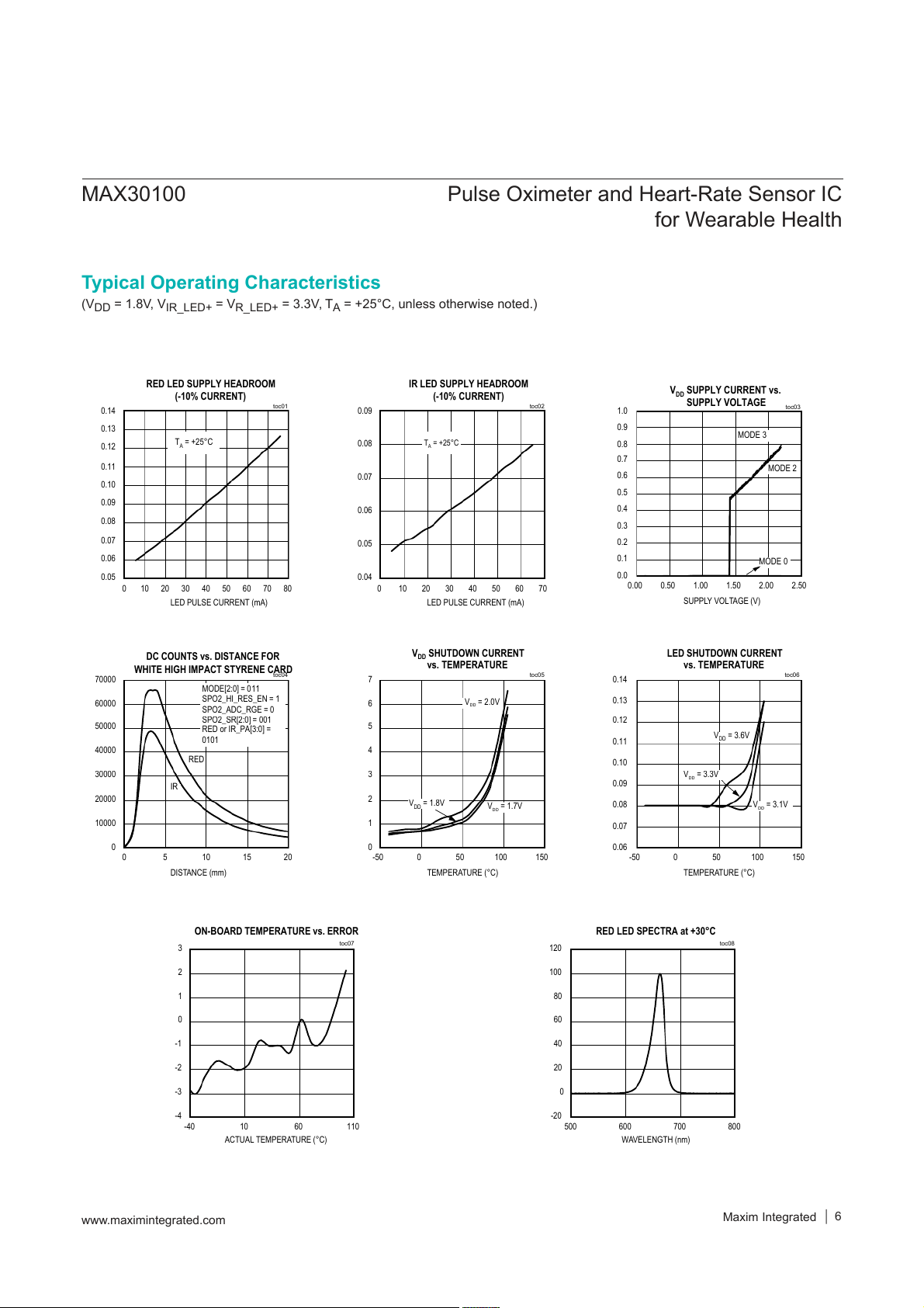
Typical Operating Characteristics (VDD = 1.8V, V = V
= 3.3V, T = +25°C, unless otherwise noted.) IR_LED+ R_LED+ A RED LED SUPPLY HEADROOM IR LED SUPPLY HEADROOM V SUPPLY CURRENT vs. DD (-10% CURRENT) (-10% CURRENT) toc01 toc02 SUPPLY VOLTAGE 0.14 0.09 1.0 toc03 0.13 0.9 MODE 3 T = +25°C A 0.08 T = +25°C A 0.8 (V) 0.12 (V) 0.7 ) 0.11 TAGE TAGE A MODE 2 0.07 0.6 (m VOL 0.10 VOL T N E 0.5 R 0.09 R 0.06 U 0.4 C 0.08 LY 0.3 P COMPLIANCE COMPLIANCE P 0.07 U 0.05 0.2 S PIN PIN 0.06 0.1 MODE 0 DRV DRV 0.05 0.04 0.0 0.00 0.50 1.00 1.50 2.00 2.50 0 10 20 30 40 50 60 70 80 0 10 20 30 40 50 60 70 LED PULSE CURRENT (mA) LED PULSE CURRENT (mA) SUPPLY VOLTAGE (V)
DC COUNTS vs. DISTANCE FOR V SHUTDOWN CURRENT LED SHUTDOWN CURRENT DD
WHITE HIGH IMPACT STYRENE CARD vs. TEMPERATURE vs. TEMPERATURE toc04 toc05 toc06 70000 7 0.14 MODE[2:0] = 011 SPO2_HI_RES_EN = 1 60000 6 V = 2.0V 0.13 SPO2_ADC_RGE = 0 DD A) SPO2_SR[2:0] = 001 (µ (µA) 0.12 50000 RED or IR_PA[3:0] = 5 V = 3.6V 0101 0.11 DD (SUM) 40000 4 RED CURRENT CURRENT 0.10 30000 3 V = 3.3V DD COUNTS IR 0.09 20000 2 SHUTDOWN V = 1.8V DD V = 1.7V SHUTDOWN 0.08 V = 3.1V D DD DD V D 10000 1 LED 0.07 0 0 0.06 0 5 10 15 20 -50 0 50 100 150 -50 0 50 100 150 DISTANCE (mm) TEMPERATURE (°C) TEMPERATURE (°C)
ON-BOARD TEMPERATURE vs. ERROR
RED LED SPECTRA at +30°C toc07 toc08 3 120 2 100 (°C) 1 (%) 80 0 60 ERROR POWER -1 TURE 40 -2 NORMALIZE 20 TEMPERA -3 0 -4 -20 -40 10 60 110 500 600 700 800 ACTUAL TEMPERATURE (°C) WAVELENGTH (nm) Maxim Integrated │ 6 www.maximintegrated.com MAX30100
Pulse Oximeter and Heart-Rate Sensor IC for Wearable Health
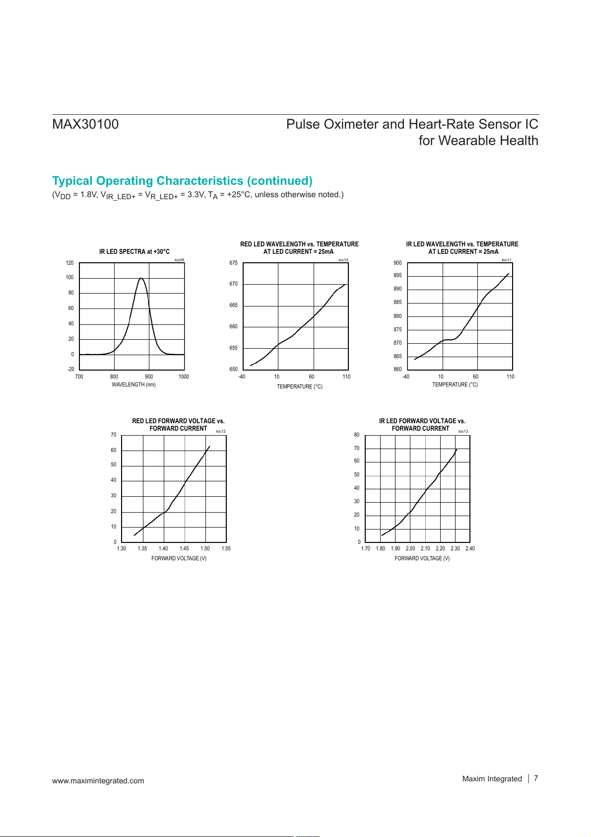
Typical Operating Characteristics (continued) (VDD = 1.8V, V = V
= 3.3V, T = +25°C, unless otherwise noted.) IR_LED+ R_LED+ A
RED LED WAVELENGTH vs. TEMPERATURE
IR LED WAVELENGTH vs. TEMPERATURE
IR LED SPECTRA at +30°C AT LED CURRENT = 25mA AT LED CURRENT = 25mA toc09 toc10 toc11 120 675 900 895 100 670 890 (%) 80 (nm) (nm) 885 665 60 POWER 880 VELENGTH VELENGTH 40 WA 660 WA 875 NORMALIZE 20 PEAK PEAK 870 655 0 865 -20 650 860 700 800 900 1000 -40 10 60 110 -40 10 60 110 WAVELENGTH (nm) TEMPERATURE (°C) TEMPERATURE (°C)
RED LED FORWARD VOLTAGE vs.
IR LED FORWARD VOLTAGE vs. FORWARD CURRENT FORWARD CURRENT toc12 toc13 70 80 60 70 60 50 50 (mA) (mA) 40 40 30 CURRENT CURRENT 30 RD 20 RD A A 20 FORW 10 FORW 10 0 0 1.30 1.35 1.40 1.45 1.50 1.55 1.70 1.80 1.90 2.00 2.10 2.20 2.30 2.40 FORWARD VOLTAGE (V) FORWARD VOLTAGE (V) Maxim Integrated │ 7 www.maximintegrated.com MAX30100
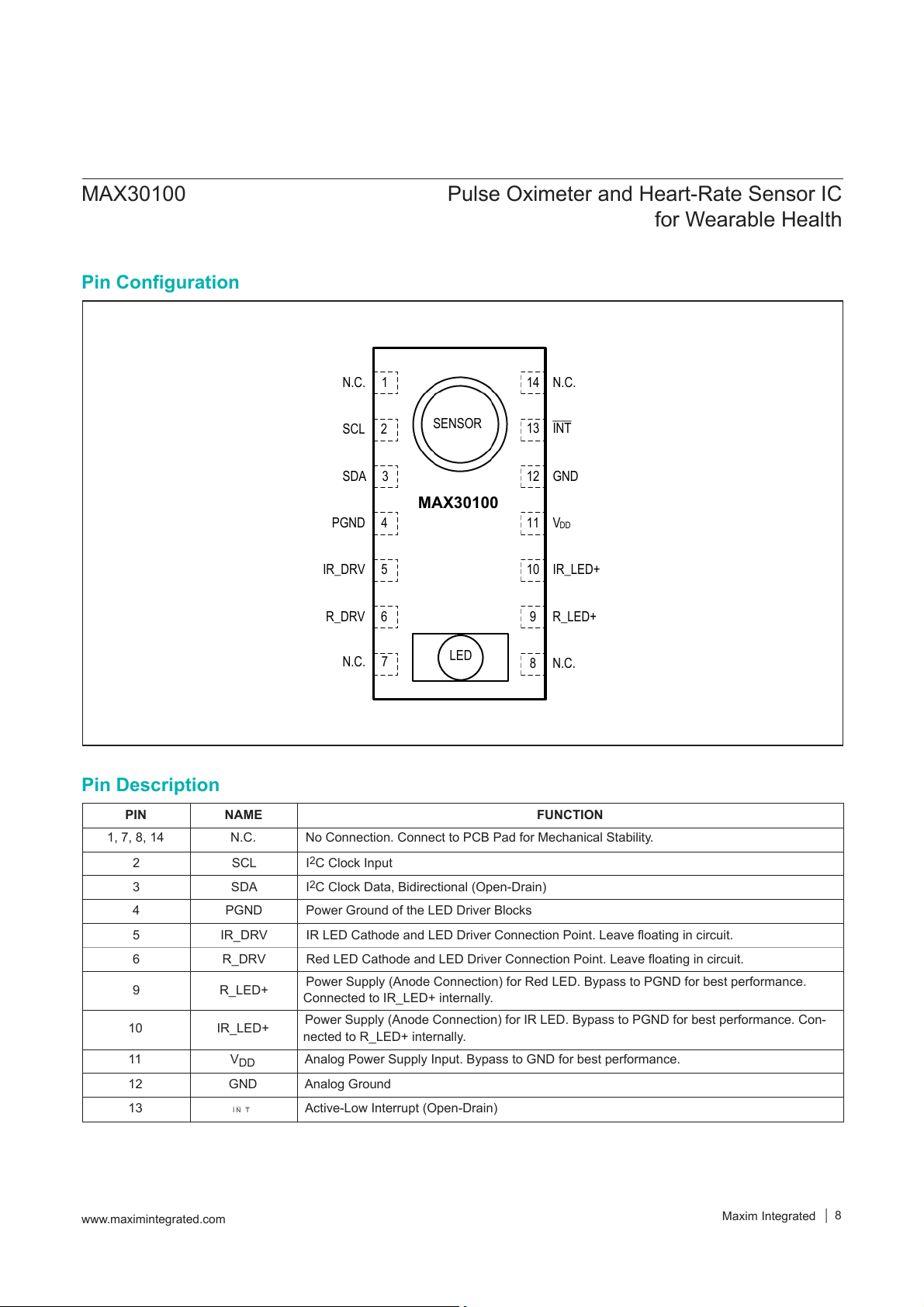
Pulse Oximeter and Heart-Rate Sensor IC for Wearable Health Pin Configuration N.C. 1 14 N.C. SCL 2 SENSOR 13 INT SDA 3 12 GND MAX30100 PGND 4 11 VDD IR_DRV 5 10 IR_LED+ R_DRV 6 9 R_LED+ N.C. 7 LED 8 N.C. Pin Description PIN NAME FUNCTION 1, 7, 8, 14 N.C.
No Connection. Connect to PCB Pad for Mechanical Stability. 2 SCL I2C Clock Input 3 SDA
I2C Clock Data, Bidirectional (Open-Drain) 4 PGND
Power Ground of the LED Driver Blocks 5 IR_DRV
IRLEDCathodeandLEDDriverConnectionPoint.Leavefloatingincircuit. 6 R_DRV
RedLEDCathodeandLEDDriverConnectionPoint.Leavefloatingincircuit.
Power Supply (Anode Connection) for Red LED. Bypass to PGND for best performance. 9 R_LED+
Connected to IR_LED+ internally.
Power Supply (Anode Connection) for IR LED. Bypass to PGND for best performance. Con- 10 IR_LED+ nected to R_LED+ internally. 11 VDD
Analog Power Supply Input. Bypass to GND for best performance. 12 GND Analog Ground 13 INT
Active-Low Interrupt (Open-Drain) www.maximintegrated.com Maxim Integrated │ 8 MAX30100
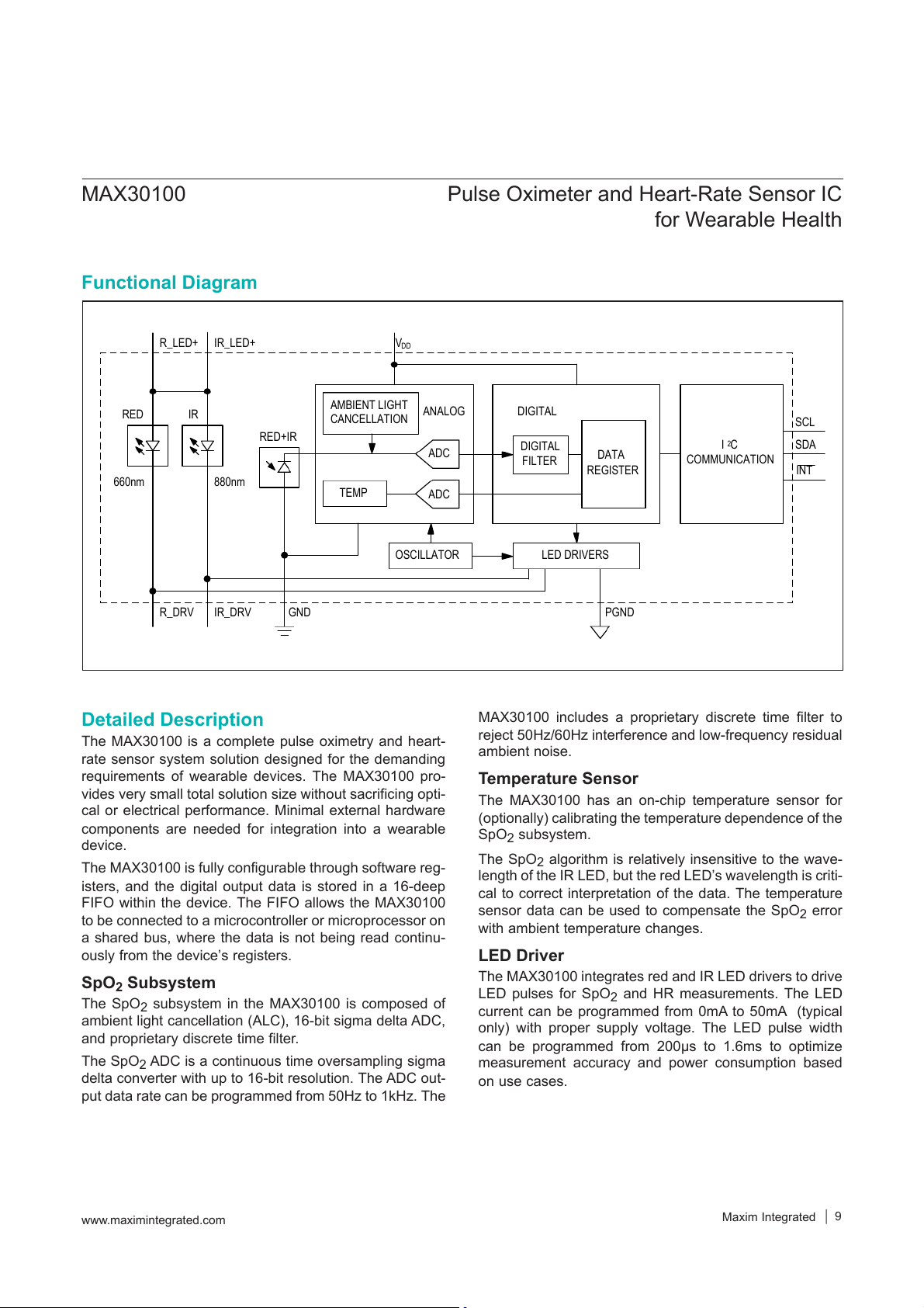
Pulse Oximeter and Heart-Rate Sensor IC for Wearable Health Functional Diagram R_LED+ IR_LED+ VDD AMBIENT LIGHT ANALOG DIGITAL RED IR CANCELLATION SCL RED+IR DIGITAL I 2C SDA ADC DATA FILTER COMMUNICATION REGISTER INT 660nm 880nm TEMP ADC OSCILLATOR LED DRIVERS R_DRV IR_DRV GND PGND Detailed Description
MAX30100 includes a proprietary discrete time filter to
The MAX30100 is a complete pulse oximetry and heart-
reject 50Hz/60Hz interference and low-frequency residual ambient noise.
rate sensor system solution designed for the demanding
requirements of wearable devices. The MAX30100 pro- Temperature Sensor
vides very small total solution size without sacrificing opti-
The MAX30100 has an on-chip temperature sensor for
cal or electrical performance. Minimal external hardware
(optionally) calibrating the temperature dependence of the
components are needed for integration into a wearable SpO2 subsystem. device.
The SpO algorithm is relatively insensitive to the wave-
The MAX30100 is fully configurable through software reg- 2
length of the IR LED, but the red LED’s wavelength is criti-
isters, and the digital output data is stored in a 16-deep
cal to correct interpretation of the data. The temperature
FIFO within the device. The FIFO allows the MAX30100
sensor data can be used to compensate the SpO error 2
to be connected to a microcontroller or microprocessor on
with ambient temperature changes.
a shared bus, where the data is not being read continu-
ously from the device’s registers. LED Driver SpO
The MAX30100 integrates red and IR LED drivers to drive 2 Subsystem
LED pulses for SpO and HR measurements. The LED 2
The SpO subsystem in the MAX30100 is composed of 2
current can be programmed from 0mA to 50mA (typical
ambient light cancellation (ALC), 16-bit sigma delta ADC,
only) with proper supply voltage. The LED pulse width
and proprietary discrete time filter.
can be programmed from 200µs to 1.6ms to optimize
The SpO ADC is a continuous time oversampling sigma 2
measurement accuracy and power consumption based
delta converter with up to 16-bit resolution. The ADC out- on use cases.
put data rate can be programmed from 50Hz to 1kHz. The www.maximintegrated.com Maxim Integrated │ 9 MAX30100
Pulse Oximeter and Heart-Rate Sensor IC for Wearable Health
Table 1. Register Maps and Descriptions REG POR REGISTER B7 B6 B5 B4 B3 B2 B1 B0 R/W ADDR STATE STATUS Interrupt TEMP_ SPO2_ PWR_ A_FULL HR_RDY 0x00 0X00 R Status RDY RDY RDY Interrupt En- ENB_A_ ENB_TE ENB_HR_ ENB_S 0x01 0X00 R/W able FULL P_RDY RDY O2_RDY FIFO FIFO Write FIFO_WR_PTR[3:0] 0x02 0x00 R/W Pointer Over Flow OVF_COUNTER[3:0] 0x03 0x00 R/W Counter FIFO Read FIFO_RD_PTR[3:0] 0x04 0x00 R/W Pointer FIFO Data FIFO_DATA[7:0] 0x05 0x00 R/W Register CONFIGURATION ModeConfigu- TEMP_ SHDN RESET MODE[2:0] 0x06 0x00 R/W ration EN SPO2Configu- SPO2_HI_ RE- SPO2_SR[2:0] LED_PW[1:0] 0x07 0x00 R/W ration RES_EN SERVED RESERVED 0x08 0x00 R/W LEDConfigura- RED_PA[3:0] IR_PA[3:0] 0x09 0x00 R/W tion 0x0A RESERVED 0x00 R/W – 0x15 TEMPERATURE Temp_Integer TINT[7:0] 0x16 0x00 R/W Temp_Fraction TFRAC[3:0] 0x17 0x00 R/W RESERVED 0x8D 0x00 R/W PART ID Revision ID REV_ID[7:0] 0xFE 0xXX* R Part ID PART_ID[7] 0xFF 0x11 R/W
*XX denotes any 2-digit hexidecimal number (00 to FF). Contact Maxim Integrated for the Revision ID number assigned for your product. www.maximintegrated.com
Maxim Integrated │ 10 MAX30100
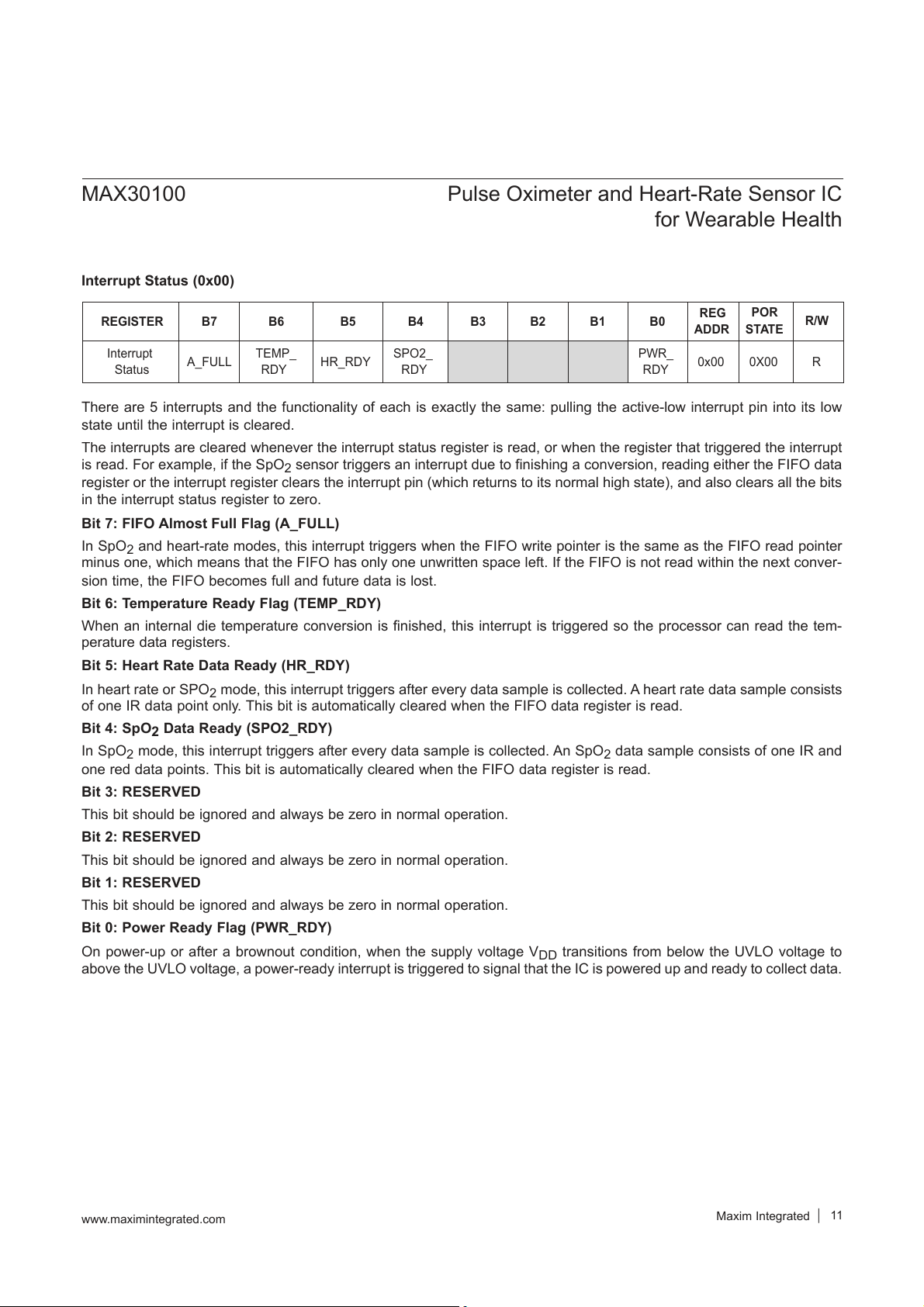
Pulse Oximeter and Heart-Rate Sensor IC for Wearable Health Interrupt Status (0x00) REG POR REGISTER B7 B6 B5 B4 B3 B2 B1 B0 R/W ADDR STATE Interrupt TEMP_ SPO2_ PWR_ A_FULL HR_RDY 0x00 0X00 R Status RDY RDY RDY
There are 5 interrupts and the functionality of each is exactly the same: pulling the active-low interrupt pin into its low
state until the interrupt is cleared.
The interrupts are cleared whenever the interrupt status register is read, or when the register that triggered the interrupt
is read. For example, if the SpO sensor triggers an interrupt due to finishing a conversion, reading either the FIFO data 2
register or the interrupt register clears the interrupt pin (which returns to its normal high state), and also clears all the bits
in the interrupt status register to zero.
Bit 7: FIFO Almost Full Flag (A_FULL)
In SpO and heart-rate modes, this interrupt triggers when the FIFO write pointer is the same as the FIFO read pointer 2
minus one, which means that the FIFO has only one unwritten space left. If the FIFO is not read within the next conver-
sion time, the FIFO becomes full and future data is lost.
Bit 6: Temperature Ready Flag (TEMP_RDY)
When an internal die temperature conversion is finished, this interrupt is triggered so the processor can read the tem- perature data registers.
Bit 5: Heart Rate Data Ready (HR_RDY)
In heart rate or SPO mode, this interrupt triggers after every data sample is collected. A heart rate data sample consists 2
of one IR data point only. This bit is automatically cleared when the FIFO data register is read.
Bit 4: SpO2 Data Ready (SPO2_RDY)
In SpO mode, this interrupt triggers after every data sample is collected. An SpO data sample consists of one IR and 2 2
one red data points. This bit is automatically cleared when the FIFO data register is read. Bit 3: RESERVED
This bit should be ignored and always be zero in normal operation. Bit 2: RESERVED
This bit should be ignored and always be zero in normal operation. Bit 1: RESERVED
This bit should be ignored and always be zero in normal operation.
Bit 0: Power Ready Flag (PWR_RDY)
On power-up or after a brownout condition, when the supply voltage V
transitions from below the UVLO voltage to DD
above the UVLO voltage, a power-ready interrupt is triggered to signal that the IC is powered up and ready to collect data. www.maximintegrated.com
Maxim Integrated │ 11 MAX30100
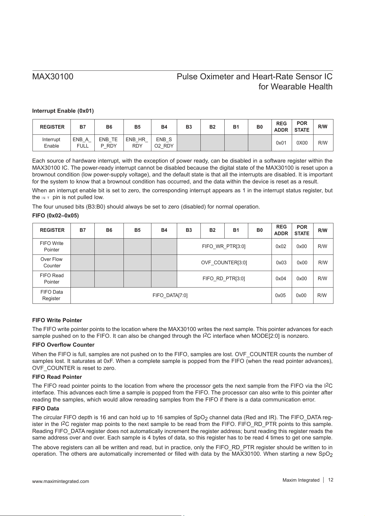
Pulse Oximeter and Heart-Rate Sensor IC for Wearable Health Interrupt Enable (0x01) REG POR REGISTER B7 B6 B5 B4 B3 B2 B1 B0 R/W ADDR STATE Interrupt ENB_A_ ENB_TE ENB_HR_ ENB_S 0x01 0X00 R/W Enable FULL P_RDY RDY O2_RDY
Each source of hardware interrupt, with the exception of power ready, can be disabled in a software register within the
MAX30100 IC. The power-ready interrupt cannot be disabled because the digital state of the MAX30100 is reset upon a
brownout condition (low power-supply voltage), and the default state is that all the interrupts are disabled. It is important
for the system to know that a brownout condition has occurred, and the data within the device is reset as a result.
When an interrupt enable bit is set to zero, the corresponding interrupt appears as 1 in the interrupt status register, but the INT pin is not pulled low.
The four unused bits (B3:B0) should always be set to zero (disabled) for normal operation. FIFO (0x02–0x05) REG POR REGISTER B7 B6 B5 B4 B3 B2 B1 B0 R/W ADDR STATE FIFO Write FIFO_WR_PTR[3:0] 0x02 0x00 R/W Pointer Over Flow OVF_COUNTER[3:0] 0x03 0x00 R/W Counter FIFO Read FIFO_RD_PTR[3:0] 0x04 0x00 R/W Pointer FIFO Data FIFO_DATA[7:0] 0x05 0x00 R/W Register FIFO Write Pointer
The FIFO write pointer points to the location where the MAX30100 writes the next sample. This pointer advances for each
sample pushed on to the FIFO. It can also be changed through the I2C interface when MODE[2:0] is nonzero. FIFO Overflow Counter
When the FIFO is full, samples are not pushed on to the FIFO, samples are lost. OVF_COUNTER counts the number of
samples lost. It saturates at 0xF. When a complete sample is popped from the FIFO (when the read pointer advances), OVF_COUNTER is reset to zero. FIFO Read Pointer
The FIFO read pointer points to the location from where the processor gets the next sample from the FIFO via the I2C
interface. This advances each time a sample is popped from the FIFO. The processor can also write to this pointer after
reading the samples, which would allow rereading samples from the FIFO if there is a data communication error. FIFO Data
The circular FIFO depth is 16 and can hold up to 16 samples of SpO channel data (Red and IR). The FIFO_DATA reg- 2
ister in the I2C register map points to the next sample to be read from the FIFO. FIFO_RD_PTR points to this sample.
Reading FIFO_DATA register does not automatically increment the register address; burst reading this register reads the
same address over and over. Each sample is 4 bytes of data, so this register has to be read 4 times to get one sample.
The above registers can all be written and read, but in practice, only the FIFO_RD_PTR register should be written to in
operation. The others are automatically incremented or filled with data by the MAX30100. When starting a new SpO2 www.maximintegrated.com
Maxim Integrated │ 12 MAX30100
Pulse Oximeter and Heart-Rate Sensor IC for Wearable Health
or heart-rate conversion, it is recommended to first clear the FIFO_WR_PTR, OVF_COUNTER, and FIFO_RD_PTR
registers to all zeros (0x00) to ensure the FIFO is empty and in a known state. When reading the MAX30100 registers
in one burst-read I2C transaction, the register address pointer typically increments so that the next byte of data sent is
from the next register, etc. The exception to this is the FIFO data register, register 0x05. When reading this register, the
address pointer does not increment, but the FIFO_RD_PTR does. So the next byte of data sent will represent the next
byte of data available in the FIFO. Reading from the FIFO
Normally, reading registers from the I2C interface autoincrements the register address pointer, so that all the registers
can be read in a burst read without an I2C restart event. In the MAX30100, this holds true for all registers except for the FIFO_DATA register (0x05).
Reading the FIFO_DATA register does not automatically increment the register address; burst reading this register reads
the same address over and over. Each sample is 4 bytes of data, so this register has to be read 4 times to get one sample.
The other exception is 0xFF, reading more bytes after the 0xFF register does not advance the address pointer back to
0x00, and the data read is not meaningful. FIFO Data Structure
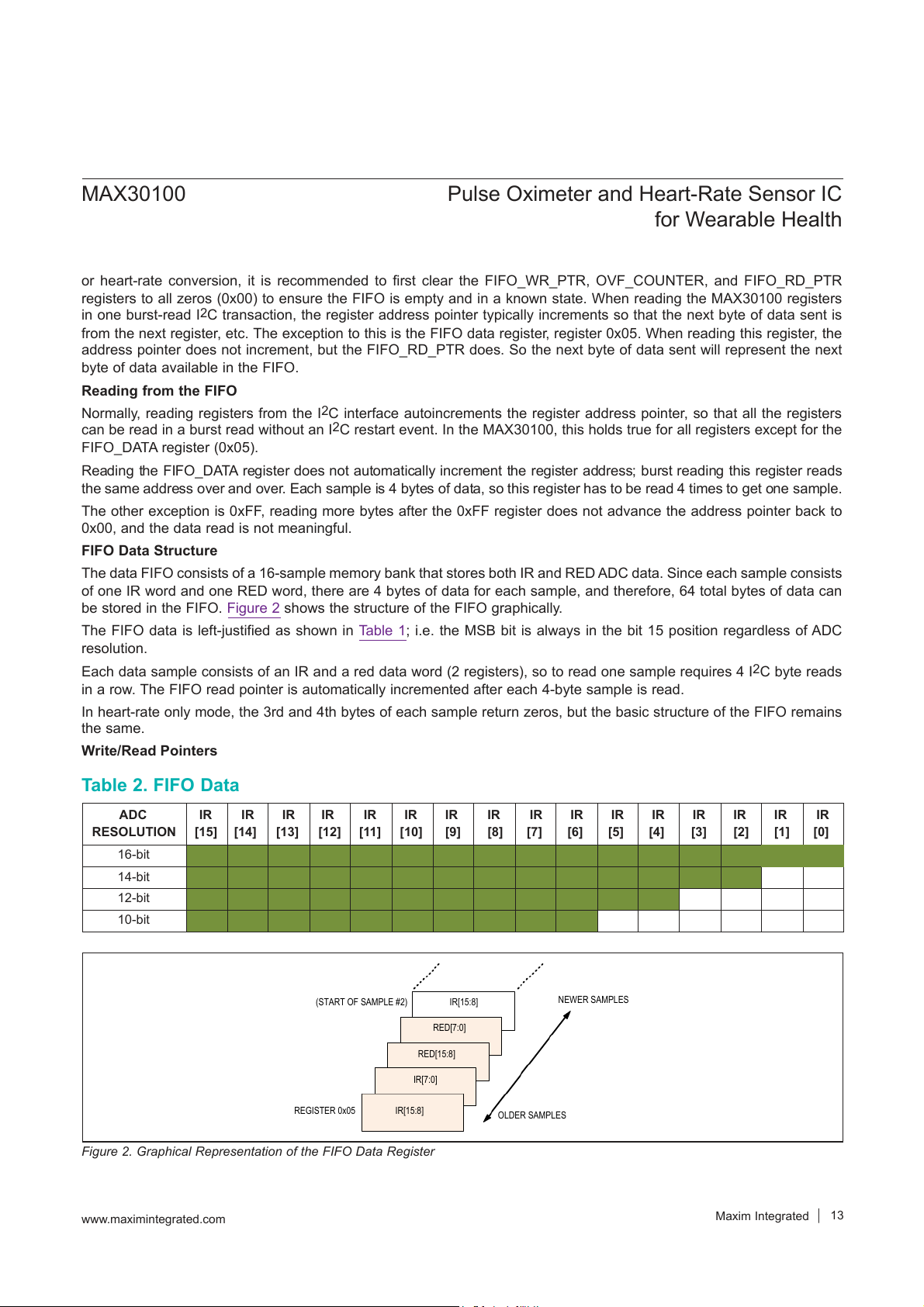
The data FIFO consists of a 16-sample memory bank that stores both IR and RED ADC data. Since each sample consists
of one IR word and one RED word, there are 4 bytes of data for each sample, and therefore, 64 total bytes of data can
be stored in the FIFO. Figure 2 shows the structure of the FIFO graphically.
The FIFO data is left-justified as shown in Table 1; i.e. the MSB bit is always in the bit 15 position regardless of ADC resolution.
Each data sample consists of an IR and a red data word (2 registers), so to read one sample requires 4 I2C byte reads
in a row. The FIFO read pointer is automatically incremented after each 4-byte sample is read.
In heart-rate only mode, the 3rd and 4th bytes of each sample return zeros, but the basic structure of the FIFO remains the same. Write/Read Pointers Table 2. FIFO Data ADC IR IR IR IR IR IR IR IR IR IR IR IR IR IR IR IR RESOLUTION [15] [14] [13] [12] [11] [10] [9] [8] [7] [6] [5] [4] [3] [2] [1] [0] 16-bit 14-bit 12-bit 10-bit NEWER SAMPLES (START OF SAMPLE #2) IR[15:8] RED[7:0] RED[15:8] IR[7:0] REGISTER 0x05 IR[15:8] OLDER SAMPLES
Figure 2. Graphical Representation of the FIFO Data Register www.maximintegrated.com
Maxim Integrated │ 13 MAX30100
Pulse Oximeter and Heart-Rate Sensor IC for Wearable Health
The locations to store new data, and the read pointer for reading data, are used to control the flow of data in the FIFO.
The write pointer increments every time a new sample is added to the FIFO. The read pointer is incremented automati-
cally every time a sample is read from the FIFO. To reread a sample from the FIFO, decrement its value by one and read the data register again.
The SpO write/read pointers should be cleared (back to 0x0) upon entering SpO mode or heart-rate mode, so that 2 2
there is no old data represented in the FIFO. The pointers are not automatically cleared when changing modes, but they are cleared if V is power cycled so that the V
voltage drops below its UVLO voltage. DD DD
Pseudo-Code Example of Reading Data from FIFO
First transaction: Get the FIFO_WR_PTR: START;
Send device address + write mode Send address of FIFO_WR_PTR; REPEATED_START;
Send device address + read mode Read FIFO_WR_PTR; STOP;
The central processor evaluates the number of samples to be read from the FIFO:
NUM_AVAILABLE_SAMPLES = FIFO_WR_PTR – FIFO_RD_PTR
(Note: pointer wrap around should be taken into account)
NUM_SAMPLES_TO_READ = < less than or equal to NUM_AVAILABLE_SAMPLES >
Second transaction: Read NUM_SAMPLES_TO_READ samples from the FIFO: START;
Send device address + write mode Send address of FIFO_DATA; REPEATED_START;
Send device address + read mode
for (i = 0; i < NUM_SAMPLES_TO_READ; i++) { Read FIFO_DATA; Save IR[15:8]; Read FIFO_DATA; Save IR[7:0]; Read FIFO_DATA; Save R[15:8]; Read FIFO_DATA; Save R[7:0]; } STOP; www.maximintegrated.com
Maxim Integrated │ 14 MAX30100
Pulse Oximeter and Heart-Rate Sensor IC for Wearable Health
Third transaction: Write to FIFO_RD_PTR register. If the second transaction was successful, FIFO_RD_PTR points
to the next sample in the FIFO, and this third transaction is not necessary. Otherwise, the processor updates the
FIFO_RD_PTR appropriately, so that the samples are reread. START;
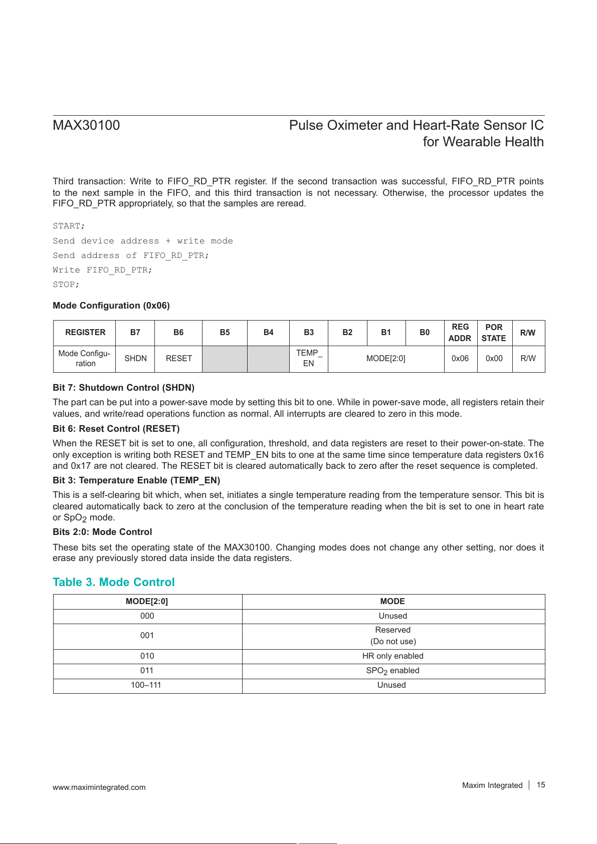
Send device address + write mode Send address of FIFO_RD_PTR; Write FIFO_RD_PTR; STOP; Mode Configuration (0x06) REG POR REGISTER B7 B6 B5 B4 B3 B2 B1 B0 R/W ADDR STATE ModeConfigu- TEMP_ SHDN RESET MODE[2:0] 0x06 0x00 R/W ration EN Bit 7: Shutdown Control (SHDN)
The part can be put into a power-save mode by setting this bit to one. While in power-save mode, all registers retain their
values, and write/read operations function as normal. All interrupts are cleared to zero in this mode.
Bit 6: Reset Control (RESET)
When the RESET bit is set to one, all configuration, threshold, and data registers are reset to their power-on-state. The
only exception is writing both RESET and TEMP_EN bits to one at the same time since temperature data registers 0x16
and 0x17 are not cleared. The RESET bit is cleared automatically back to zero after the reset sequence is completed.
Bit 3: Temperature Enable (TEMP_EN)
This is a self-clearing bit which, when set, initiates a single temperature reading from the temperature sensor. This bit is
cleared automatically back to zero at the conclusion of the temperature reading when the bit is set to one in heart rate or SpO mode. 2 Bits 2:0: Mode Control
These bits set the operating state of the MAX30100. Changing modes does not change any other setting, nor does it
erase any previously stored data inside the data registers. Table 3. Mode Control MODE[2:0] MODE 000 Unused Reserved 001 (Do not use) 010 HR only enabled 011 SPO2 enabled 100–111 Unused www.maximintegrated.com
Maxim Integrated │ 15 MAX30100
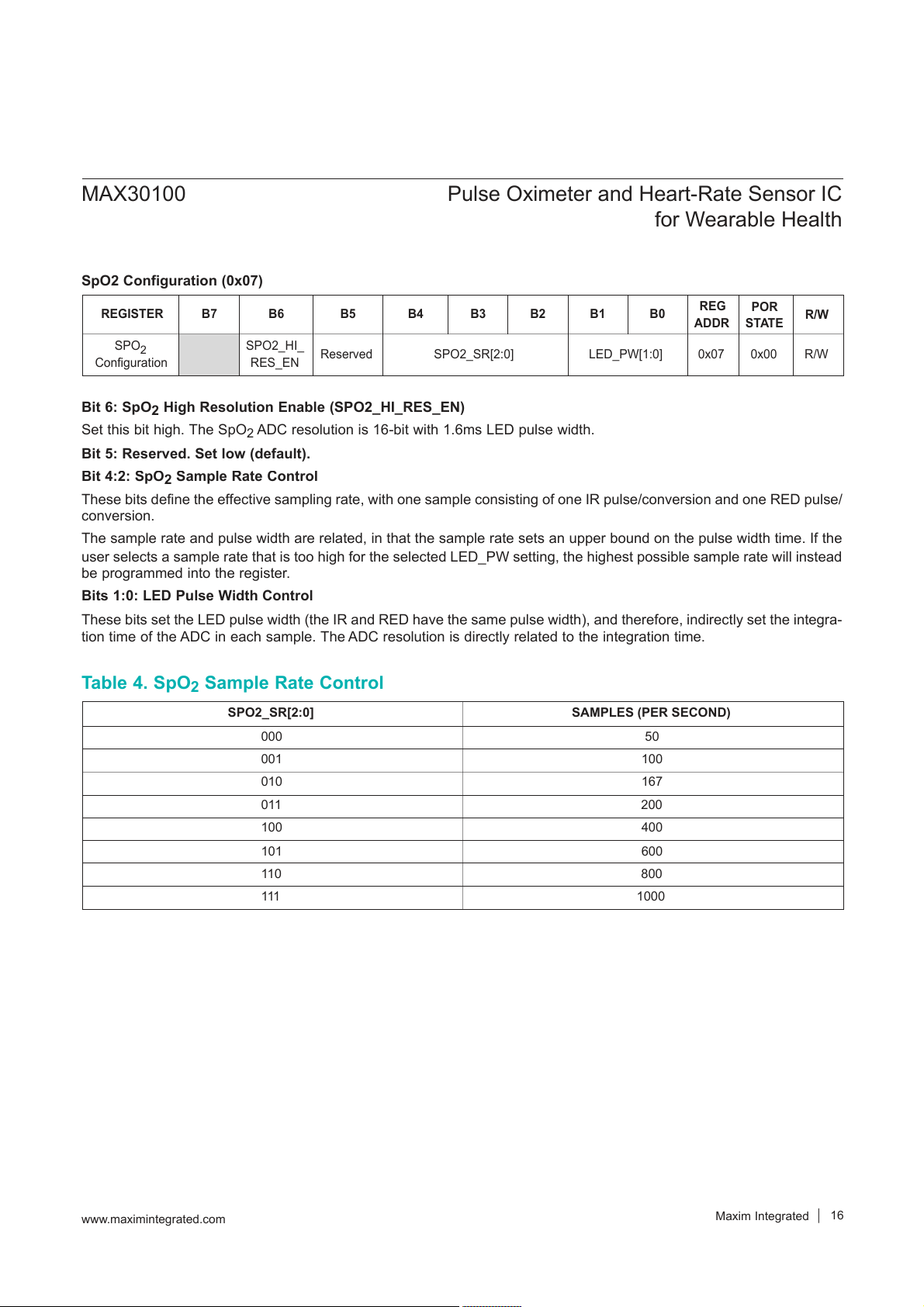
Pulse Oximeter and Heart-Rate Sensor IC for Wearable Health SpO2 Configuration (0x07) REG POR REGISTER B7 B6 B5 B4 B3 B2 B1 B0 R/W ADDR STATE SPO2 SPO2_HI_ Reserved SPO2_SR[2:0] LED_PW[1:0] 0x07 0x00 R/W Configuration RES_EN
Bit 6: SpO2 High Resolution Enable (SPO2_HI_RES_EN)
Set this bit high. The SpO ADC resolution is 16-bit with 1.6ms LED pulse width. 2
Bit 5: Reserved. Set low (default).
Bit 4:2: SpO Sample Rate Control 2
These bits define the effective sampling rate, with one sample consisting of one IR pulse/conversion and one RED pulse/ conversion.
The sample rate and pulse width are related, in that the sample rate sets an upper bound on the pulse width time. If the
user selects a sample rate that is too high for the selected LED_PW setting, the highest possible sample rate will instead
be programmed into the register.
Bits 1:0: LED Pulse Width Control
These bits set the LED pulse width (the IR and RED have the same pulse width), and therefore, indirectly set the integra-
tion time of the ADC in each sample. The ADC resolution is directly related to the integration time.
Table 4. SpO2 Sample Rate Control SPO2_SR[2:0] SAMPLES (PER SECOND) 000 50 001 100 010 167 011 200 100 400 101 600 110 800 111 1000 www.maximintegrated.com
Maxim Integrated │ 16 MAX30100
Pulse Oximeter and Heart-Rate Sensor IC for Wearable Health
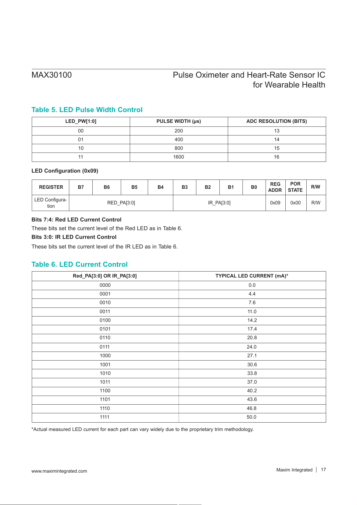
Table 5. LED Pulse Width Control LED_PW[1:0] PULSE WIDTH (µs) ADC RESOLUTION (BITS) 00 200 13 01 400 14 10 800 15 11 1600 16 LED Configuration (0x09) REG POR REGISTER B7 B6 B5 B4 B3 B2 B1 B0 R/W ADDR STATE LEDConfigura- RED_PA[3:0] IR_PA[3:0] 0x09 0x00 R/W tion
Bits 7:4: Red LED Current Control
These bits set the current level of the Red LED as in Table 6.
Bits 3:0: IR LED Current Control
These bits set the current level of the IR LED as in Table 6. Table 6. LED Current Control Red_PA[3:0] OR IR_PA[3:0]
TYPICAL LED CURRENT (mA)* 0000 0.0 0001 4.4 0010 7.6 0011 11.0 0100 14.2 0101 17.4 0110 20.8 0111 24.0 1000 27.1 1001 30.6 1010 33.8 1011 37.0 1100 40.2 1101 43.6 1110 46.8 1111 50.0
*Actual measured LED current for each part can vary widely due to the proprietary trim methodology. www.maximintegrated.com
Maxim Integrated │ 17 MAX30100
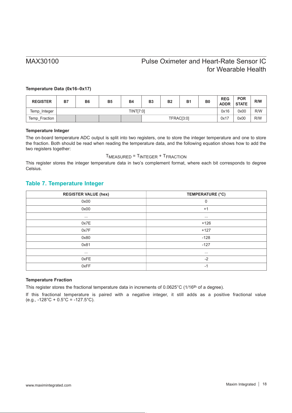
Pulse Oximeter and Heart-Rate Sensor IC for Wearable Health Temperature Data (0x16–0x17) REG POR REGISTER B7 B6 B5 B4 B3 B2 B1 B0 R/W ADDR STATE Temp_Integer TINT[7:0] 0x16 0x00 R/W Temp_Fraction TFRAC[3:0] 0x17 0x00 R/W Temperature Integer
The on-board temperature ADC output is split into two registers, one to store the integer temperature and one to store
the fraction. Both should be read when reading the temperature data, and the following equation shows how to add the two registers together: TMEASURED = T + T INTEGER FRACTION
This register stores the integer temperature data in two’s complement format, where each bit corresponds to degree Celsius. Table 7. Temperature Integer REGISTER VALUE (hex) TEMPERATURE (°C) 0x00 0 0x00 +1 ... ... 0x7E +126 0x7F +127 0x80 -128 0x81 -127 ... ... 0xFE -2 0xFF -1 Temperature Fraction
This register stores the fractional temperature data in increments of 0.0625NC (1/16th of a degree).
If this fractional temperature is paired with a negative integer, it still adds as a positive fractional value
(e.g., -128°C + 0.5°C = -127.5°C). www.maximintegrated.com
Maxim Integrated │ 18 MAX30100
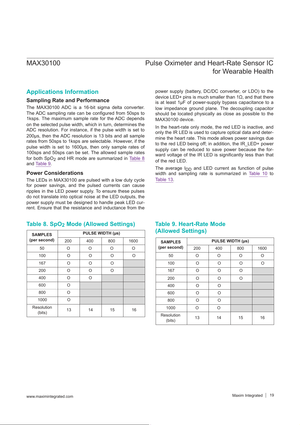
Pulse Oximeter and Heart-Rate Sensor IC for Wearable Health Applications Information
power supply (battery, DC/DC converter, or LDO) to the
deviceLED+pinsismuchsmallerthan1Ω,andthatthere Sampling Rate and Performance
is at least 1µF of power-supply bypass capacitance to a
The MAX30100 ADC is a 16-bit sigma delta converter.
low impedance ground plane. The decoupling capacitor
The ADC sampling rate can be configured from 50sps to
should be located physically as close as possible to the
1ksps. The maximum sample rate for the ADC depends MAX30100 device.
on the selected pulse width, which in turn, determines the
In the heart-rate only mode, the red LED is inactive, and
ADC resolution. For instance, if the pulse width is set to
only the IR LED is used to capture optical data and deter-
200µs, then the ADC resolution is 13 bits and all sample
mine the heart rate. This mode allows power savings due
rates from 50sps to 1ksps are selectable. However, if the
to the red LED being off; in addition, the IR_LED+ power
pulse width is set to 1600µs, then only sample rates of
supply can be reduced to save power because the for-
100sps and 50sps can be set. The allowed sample rates
ward voltage of the IR LED is significantly less than that
for both SpO and HR mode are summarized in 2 Table 8 of the red LED. and Table 9. The average I
and LED current as function of pulse DD Power Considerations
width and sampling rate is summarized in Table 10 to
The LEDs in MAX30100 are pulsed with a low duty cycle Table 13.
for power savings, and the pulsed currents can cause
ripples in the LED power supply. To ensure these pulses
do not translate into optical noise at the LED outputs, the
power supply must be designed to handle peak LED cur-
rent. Ensure that the resistance and inductance from the
Table 8. SpO2 Mode (Allowed Settings) Table 9. Heart-Rate Mode (Allowed Settings) SAMPLES PULSE WIDTH (µs) (per second) 200 400 800 1600 SAMPLES PULSE WIDTH (µs) 50 O O O O (per second) 200 400 800 1600 100 O O O O 50 O O O O 167 O O O 100 O O O O 200 O O O 167 O O O 400 O O 200 O O O 600 O 400 O O 800 O 600 O O 1000 O 800 O O Resolution 1000 O O 13 14 15 16 (bits) Resolution 13 14 15 16 (bits) www.maximintegrated.com
Maxim Integrated │ 19 MAX30100
Pulse Oximeter and Heart-Rate Sensor IC for Wearable Health
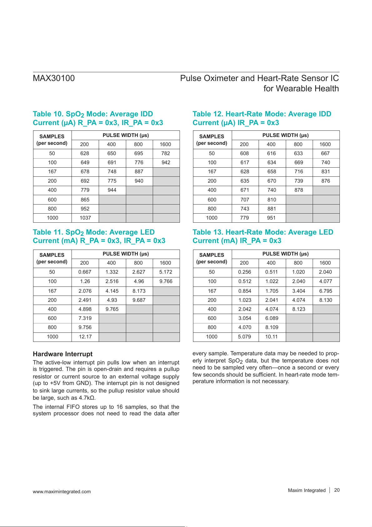
Table 10. SpO2 Mode: Average IDD
Table 12. Heart-Rate Mode: Average IDD
Current (µA) R_PA = 0x3, IR_PA = 0x3 Current (µA) IR_PA = 0x3 SAMPLES PULSE WIDTH (µs) SAMPLES PULSE WIDTH (µs) (per second) (per second) 200 400 800 1600 200 400 800 1600 50 628 650 695 782 50 608 616 633 667 100 649 691 776 942 100 617 634 669 740 167 678 748 887 167 628 658 716 831 200 692 775 940 200 635 670 739 876 400 779 944 400 671 740 878 600 865 600 707 810 800 952 800 743 881 1000 1037 1000 779 951
Table 11. SpO2 Mode: Average LED
Table 13. Heart-Rate Mode: Average LED
Current (mA) R_PA = 0x3, IR_PA = 0x3 Current (mA) IR_PA = 0x3 SAMPLES PULSE WIDTH (µs) SAMPLES PULSE WIDTH (µs) (per second) (per second) 200 400 800 1600 200 400 800 1600 50 0.667 1.332 2.627 5.172 50 0.256 0.511 1.020 2.040 100 1.26 2.516 4.96 9.766 100 0.512 1.022 2.040 4.077 167 2.076 4.145 8.173 167 0.854 1.705 3.404 6.795 200 2.491 4.93 9.687 200 1.023 2.041 4.074 8.130 400 4.898 9.765 400 2.042 4.074 8.123 600 7.319 600 3.054 6.089 800 9.756 800 4.070 8.109 1000 12.17 1000 5.079 10.11 Hardware Interrupt
every sample. Temperature data may be needed to prop-
The active-low interrupt pin pulls low when an interrupt
erly interpret SpO data, but the temperature does not 2
is triggered. The pin is open-drain and requires a pullup
need to be sampled very often—once a second or every
resistor or current source to an external voltage supply
few seconds should be sufficient. In heart-rate mode tem-
(up to +5V from GND). The interrupt pin is not designed
perature information is not necessary.
to sink large currents, so the pullup resistor value should
belarge,suchas4.7kΩ.
The internal FIFO stores up to 16 samples, so that the
system processor does not need to read the data after www.maximintegrated.com
Maxim Integrated │ 20
Tài liệu liên quan:
-
Tóm tắt lý thuyết môn IoT và ứng dụng | Học viện Công Nghệ Bưu Chính Viễn Thông
23 12 -

Accelerated Corner-Detector Algorithms: GPU Implementations and Results | Iot và ứng dụng | Học viện Công nghệ Bưu chính Viễn thông
46 23 -
Đề xuất Dự án IoT: Thiết bị phát hiện chạm cho xe máy | Iot và ứng dụng | Học viện Công nghệ Bưu chính Viễn thông
35 18 -
Phân Tích và Giải Pháp FastAPI | Iot và ứng dụng | Học viện Công nghệ Bưu chính Viễn thông
30 15 -
Tăng cường pháp chế xã hội chủ nghĩa trong quản lý nhà nước | Iot và ứng dụng | Học viện Công nghệ Bưu chính Viễn thông
25 13