Báo cáo dự án Mạch khuếch đại âm thanh môn Mạch điện tử | Trường Đại học Bách Khoa Hà Nội
In our audio amplifier circuit, we use voltage-divider bias configuration. The reason to choose this configuration is because this configuration is less dependent on or in fact is independent of the current gain β. Tài liệu được sưu tầm gồm 24 trang, giúp các bạn ôn luyện và phục vụ cho việc học tập, đạt kết quả tốt. Mời các bạn đón xem!
Môn: Mạch điện tử 14 tài liệu
Trường: Đại học Bách Khoa Hà Nội 5.8 K tài liệu
Tác giả:


Preview text:
TRƯỜNG ĐẠI HỌC BÁCH KHOA HÀ NỘI
VIỆN ĐIỆN TỬ - VIỄN THÔNG PROJECT ELECTRONIC CIRCUIT I
PRODUCT: AUDIO AMPLIFIER CIRCUIT
Instructor: Prof Phung Kieu Ha Group: 7 Class: CTTT-ĐTVT.01
Member: Nguyễn Thế Lộc 20193227 Cấn Đức Thịnh 20193238 Dương Đức Mạnh 20193229
Anagipura Tharika Gimhani 20180289 Hà Nội, 6-2022 CONTENT
LIST OF FIGURES............................................................................3
CHAPTER 1. ABTRACT THEORY OF THE PROJECT.............4
1. DC biasing on BJT’s theorem...........................................................................................4
2. BJT AC analysis’s theorem...............................................................................................6
3. Frequency response...........................................................................................................9
4. Power amplifier...............................................................................................................11
CHAPTER 2. DESIGN ........................................................................
2.1. Problem analysis..........................................................................................................13
2.2. Block diagram..............................................................................................................13
2.3 Power amplifier.............................................................................................................14 2.3.1.
DC mode................................................................................................................14
2.3.1.1. Stage 1................................................................................................................14
2.3.1.1. Stage 2................................................................................................................16
2.3.2. AC mode................................................................................................................16
2.3.2.1. Stage 1................................................................................................................16
2.3.2.2. Stage 2................................................................................................................17
2.4. Current amplifier.........................................................................................................17
2.5. Capacitor calculation...................................................................................................18
2.6. Voltage amplifier..........................................................................................................19
2.7. Complete circuit and simulation..................................................................................20
2.7.1. Total gain...............................................................................................................20
2.7.2. Result.....................................................................................................................20
REFERENCE MATERIALS...........................................................22
................................................................................................................. LIST OF FIGURES
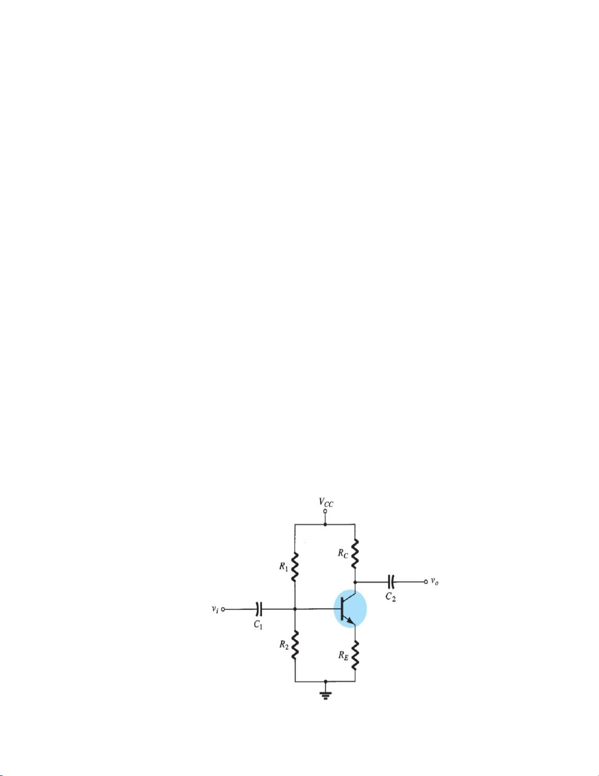
Fig1.1 Voltage-divider bias configuration
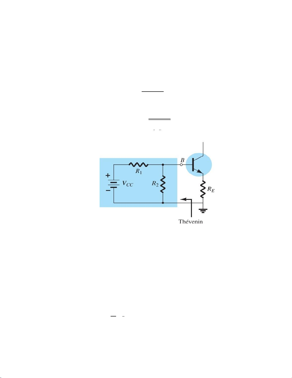
Fig1.2 Redrawing the input side of the network of Fig1.1
Fig1.3 Inserting Thevenin equivalent circuit
Fig1.4 Voltage-divider bias configuration
Fig1.4 Voltage-divider bias configuration
Fig1.5 The re equivalent circuit into the ac equivalent network of Fig1.4
Fig1.6 The re equivalent circuit into the AC equivalent network of unbypassed configurations
Fig1.7 BJT amplifier with capacitors that affect the low- frequency response.
Fig1.8 Determining the effect of C_S on the low- frequency response.
Fig1.9 Determining the effect of C_S on the low- frequency response.
Fig1.10 Localized ac equivalent of C_E
Fig1.11 Class AB Amplifier Diode Biasing Fig2.1 The first stage Fig2.2 Stage 2 Fig2.3 Stage 3 Fig2.4 Power amplifier
Fig2.5 Complete circuit of audio amplifier
Fig2.6 Output and input signal Fig2.7 Average output power
CHAPTER 1. ABTRACT THEORY OF THE PROJECT
1.1. DC biasing- BJT’s theorem
In our audio amplifier circuit, we use voltage-divider bias configuration. The
reason to choose this configuration is because this configuration is less dependent on or
in fact is independent of the current gain β. The sensitivity to changes in beta is quite
small when the temperature increases. The Fig1.1 shows the voltage-divider bias configuration.
Fig1.1 Voltage-divider bias configuration Circuit analysis
By using the Thevenin’s theorem we have: Rth: R1R2 𝑅𝑡ℎ = R1 + R2 Eth: R2 𝐸𝑡ℎ = 𝑉𝑡ℎ = 𝑉𝑐𝑐 R1 + R2
Fig1.2 Redrawing the input side of the network of Fig1.1
The Thevenin network is then redrawn as shown in Fig1.2, and 𝐼𝑐𝑄 can be
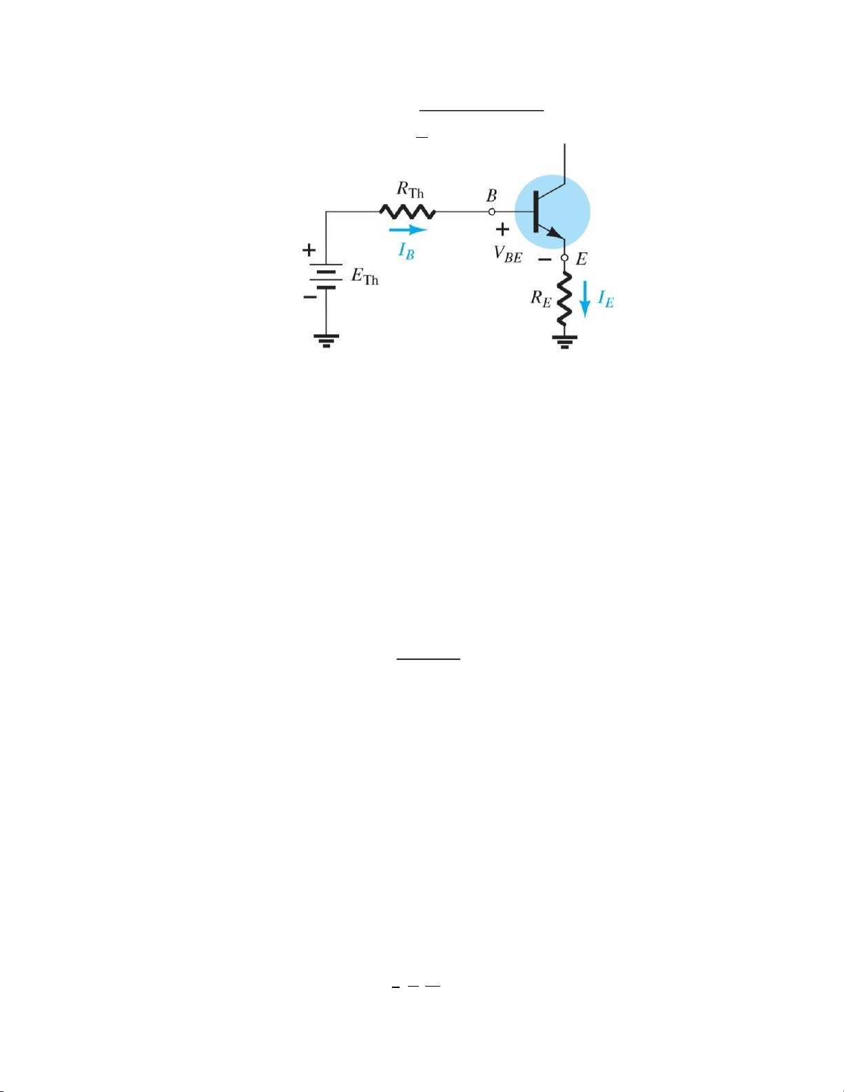
determined by first applying Kirchhoff’s voltage law in the clockwise direction for the loop indicated (Fig1.3):
𝐸𝑡ℎ − 𝐼𝐵 𝑅𝑡ℎ − 𝑉𝐵𝐸 − 𝐼𝐸 𝑅𝐸 = 0
And 𝐼𝑐𝑄 = β𝐼𝐵 , 𝐼𝑄𝑐 = 𝐼β+1𝐸 Then we have 𝐸𝑡ℎ − 𝑉𝐵𝐸
𝐼𝑐𝑄 = 𝑅𝑡ℎβ + (1 + 𝛽 𝑅) 𝐸
Fig1.3 Inserting Thevenin equivalent circuit
𝑉𝐶𝐸 of the circuit can be calculated by the following equation:
𝑉𝐶𝐸 = 𝑉𝐶𝐶 − 𝐼𝑐𝑄(𝑅𝐶 + 𝑅𝐸)
Where β + 1 ≈ β because beta is quite big Approximate analysis
The voltage across R2, which is actually the base voltage, can be determined by the following equation: R2 𝑉𝐵 = 𝑉𝑐𝑐 R1 + R2
Because 𝑅𝑖 = (β + 1)𝑅𝐸 ≈ β𝑅𝐸 the condition that will define whether the
approximate approach can be applied is: β𝑅𝐸 ≥ 10𝑅2
Once 𝑉𝐵 is determined, the level of emitter voltage can be calculated from:
𝑉𝐸 = 𝑉𝐵 − 𝑉𝐵𝐸
and the emitter current can be determined from:
𝐼𝐸 = 𝑅𝑉 𝐸𝐸 and 𝐼𝐸 ≈ 𝐼𝑐𝑄
The collector-to-emitter voltage is determined by
𝑉𝐶𝐸 = 𝑉𝐶𝐶 − 𝐼𝑐𝑅𝐶 − 𝐼𝐸 𝑅𝐸
but because 𝐼𝐸 ≈ 𝐼𝑐𝑄
𝑉𝐶𝐸 = 𝑉𝐶𝐶 − 𝐼𝑐𝑄(𝑅𝐶 + 𝑅𝐸)
1.2. BJT AC analysis’s theorem
The aim of any small signal amplifier is to amplify all of the input signal with the
minimum amount of distortion possible to the output signal, in other words, the output
signal must be an exact reproduction of the input signal but only bigger (amplified).The
Common Emitter also have the highest voltage gain in three types of common configuration.
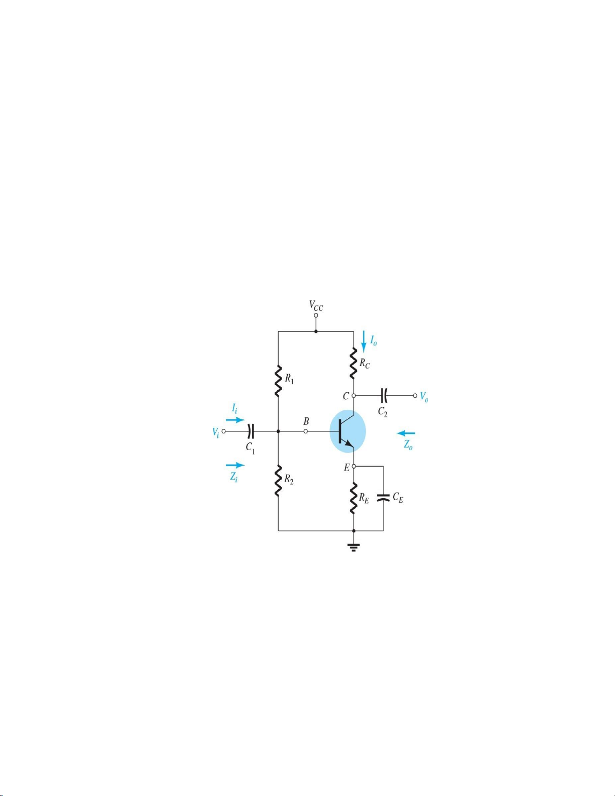
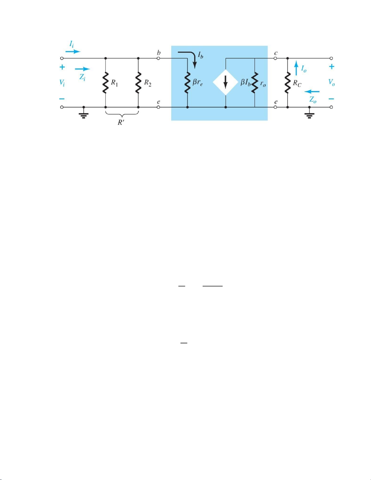
Fig1.4 Voltage-divider bias configuration
Fig1.5 The 𝑟𝑒 equivalent circuit into the ac equivalent network of Fig1.4 The input impedance 𝑍𝑖
𝑍𝑖 = 𝑅1||𝑅2||β𝑟𝑒 The output impedance 𝑍𝑜
𝑍𝑜 = 𝑟𝑜 ||𝑅𝐶
If 𝑟𝑜 ≥ 10𝑅𝐶, then: 𝑍𝑜 = 𝑅𝐶 The voltage gain 𝐴𝑉 𝑉𝑜 𝑅𝑐||𝑟𝑜
𝐴𝑉 = 𝑉 𝑖 = − 𝑟𝑒
If 𝑟𝑜 ≥ 10𝑅𝐶,then 𝑉𝑜 𝑅𝑐
𝐴𝑉 = 𝑉 𝑖 ≈ −𝑟𝑒 Unbypassed
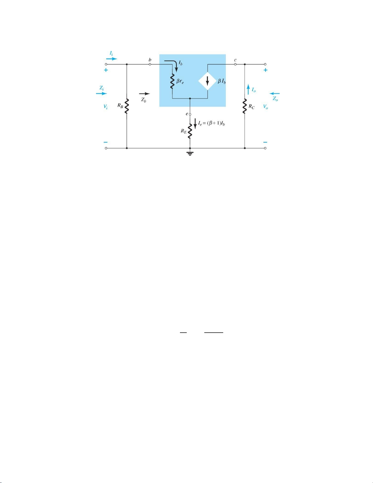
Fig1.6 The 𝑟𝑒 equivalent circuit into the AC equivalent
network of unbypassed configurations
The input impedance of a transistor with an unbypassed resistor 𝑅𝐸 is determined by
𝑍𝑏 = (β + 1)𝑅𝐸 + β𝑟𝑒
or 𝑍𝑏 ≈ (𝑅𝐸 + 𝑟𝑒 )β and 𝑍𝑏 ≈ 𝑅𝐸β if 𝑅𝐸 ≫ 𝑟𝑒 The input impedance 𝑍𝑖
𝑍𝑖 = 𝑅𝐵 ||𝑍𝑏 The output impedance 𝑍𝑜 𝑍𝑜 = 𝑅𝐶
The voltage gain 𝐴𝑉 with substituting 𝑍𝑏 ≈ (𝑅𝐸 + 𝑟𝑒 )β gives 𝑉𝑜 𝑅𝑐 𝐴𝑉 = = − 𝑉 𝑖 𝑅 𝐸+ 𝑟𝑒
1.3. Frequency response
Frequency response of an amplifier shows how the gain of output responds to input
signals at different frequencies.
Most modern audio amplifiers have a flat frequency response as shown above over
the whole audio range of frequencies from 20 Hz to 20 kHz.
In our design, we need capacitors with some following purpose:
• AC-coupled capacitors connect with input and output of overall amplifier
• Inter-stage capacitors transfer AC signals between amplifiers and provide DC isolation
• Bypass capacitors are used to get maximum voltage gain from the two inverting amplifiers
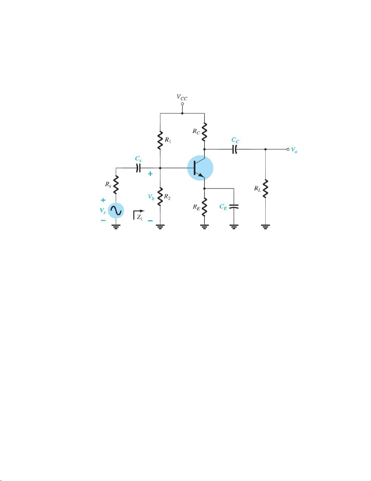
Fig1.7 BJT amplifier with capacitors that
affect the low- frequency response.
The capacitors 𝐶𝑆, 𝐶𝐶 , and 𝐶𝐸 will determine the low-frequency response following the
analysis of low-frequency response. That means when we know the value of capacitor and
the value of input and output impedance, we can calculate the frequencies affecting each
capacitor and each stage. We will now examine the impact of each independently in the order listed.
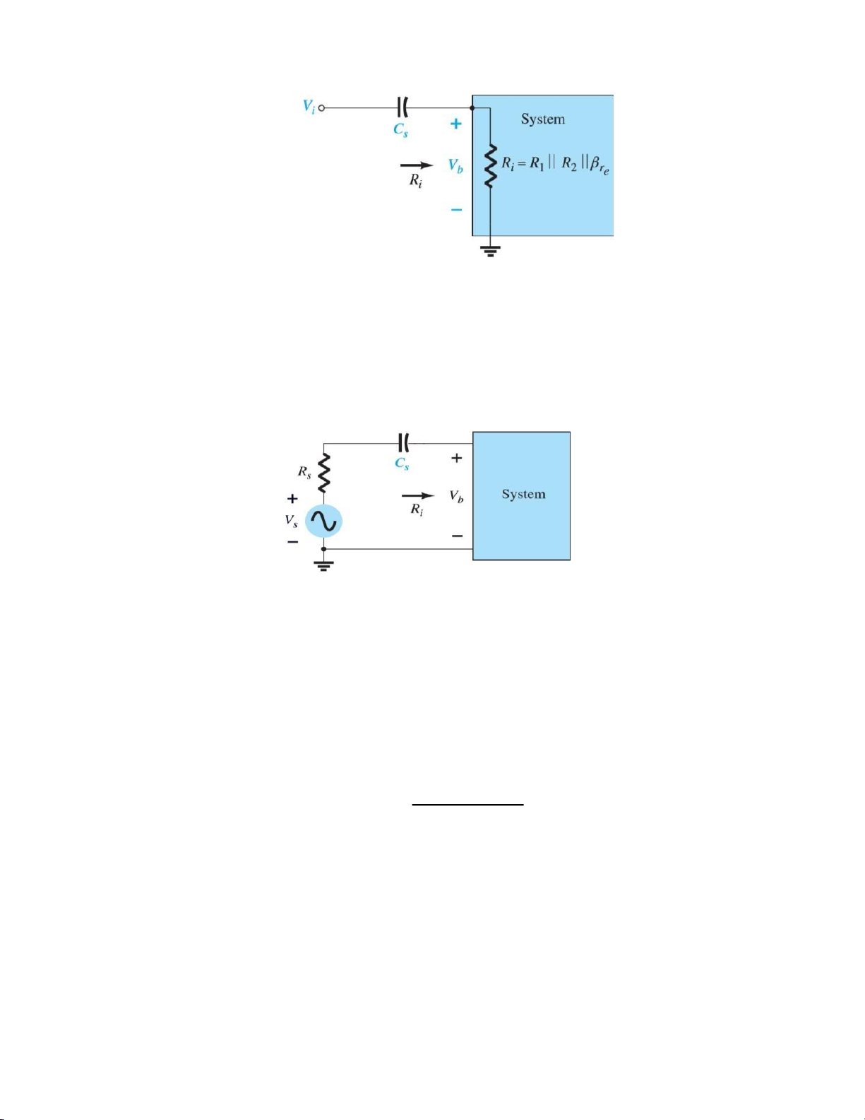
Firstly, 𝐶𝑆 is connected between the applied source and the active device matching with
𝑅𝑖 = 𝑅1||𝑅2||β𝑟𝑒
Fig1.8 Determining the effect of
𝐶𝑆 on the low- frequency response.
Fig1.9 Determining the effect of
𝐶𝑆 on the low- frequency response.
Then the frequency response of 𝐶𝑆 is:
𝑓𝐿𝑆 = 2 (𝜋 𝑅 +1 𝑅 𝐶) 𝑖 𝑠 𝑆
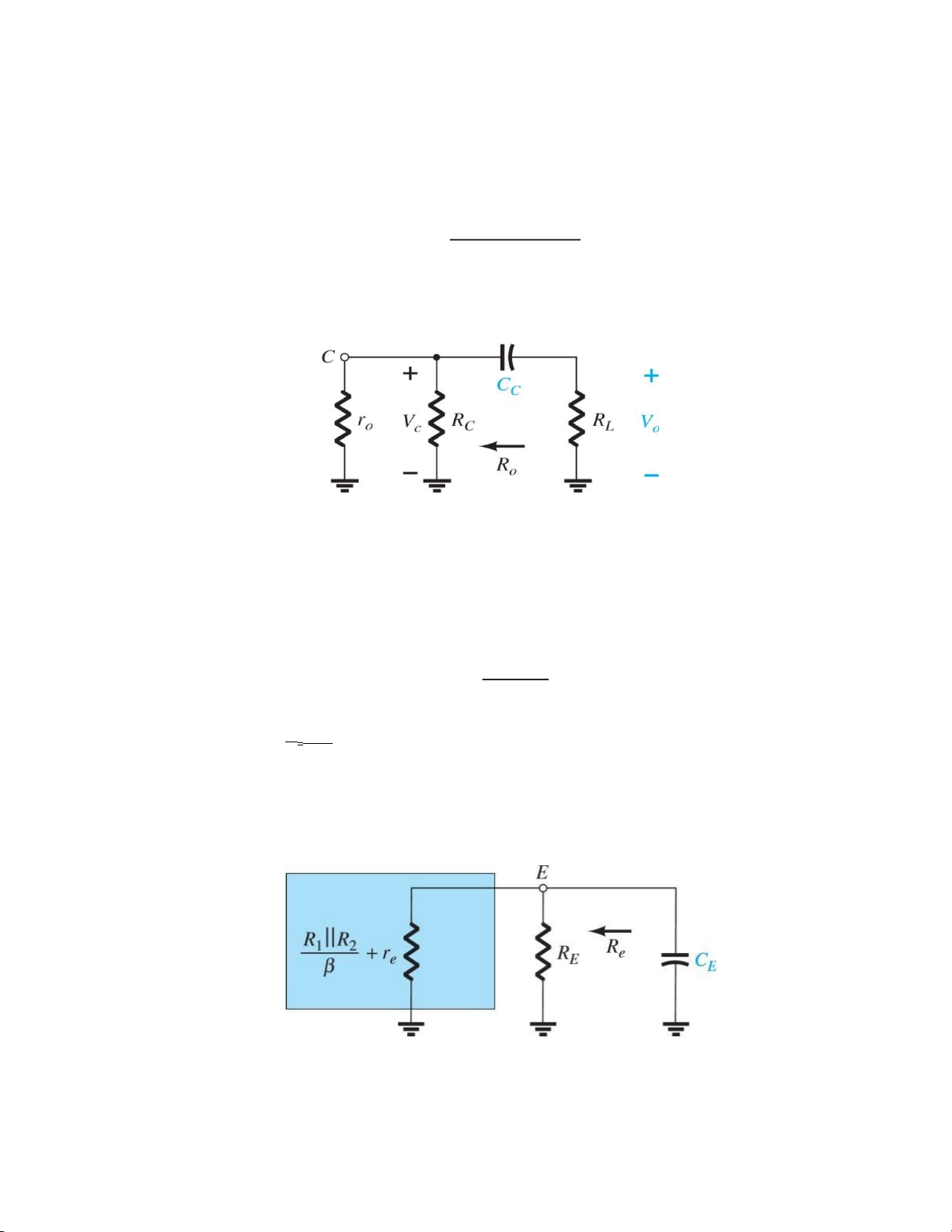
Secondly, 𝐶𝐶 the coupling capacitor is normally connected between the output of the
active device and the applied load, then the cutoff frequency due to 𝐶𝐶 is determined by: 1
𝑓𝐿𝐶 = 2 (𝜋𝑅 𝑂 + 𝑅𝐿 )𝐶𝐶
With 𝑅𝑂 = 𝑅𝐶 ||𝑟𝑜
Fig1.9 Localized ac equivalent for 𝐶𝐶 with 𝑉𝑖 = 0𝑉
Thirdly, 𝐶𝐸 bypass capacitor, the cutoff frequency due to 𝐶𝐸 can be determined using the following equation: 1
𝑓𝐿𝐸 = 2𝜋𝑅 𝑒 𝐶𝐸
Where 𝑅 = 𝑅 ||( 𝑅1 ||𝑅2 + 𝑟 ) 𝑒 𝐸 𝛽 𝑒
Fig1.10 Localized ac equivalent of 𝐶𝐸 1.4. Power amplifier
Class AB: The amplifiers two output transistors conduct somewhere between 180
degree and 360 degrees of the input waveform. And there are several types of power amplifier such as:
• Class AB Amplifier Voltage Biasing
• Class AB Amplifier Resistor Biasing
• Adjustable Amplifier Biasing
• Class AB Amplifier Diode Biasing
• Class AB Amplifier Driver Stage
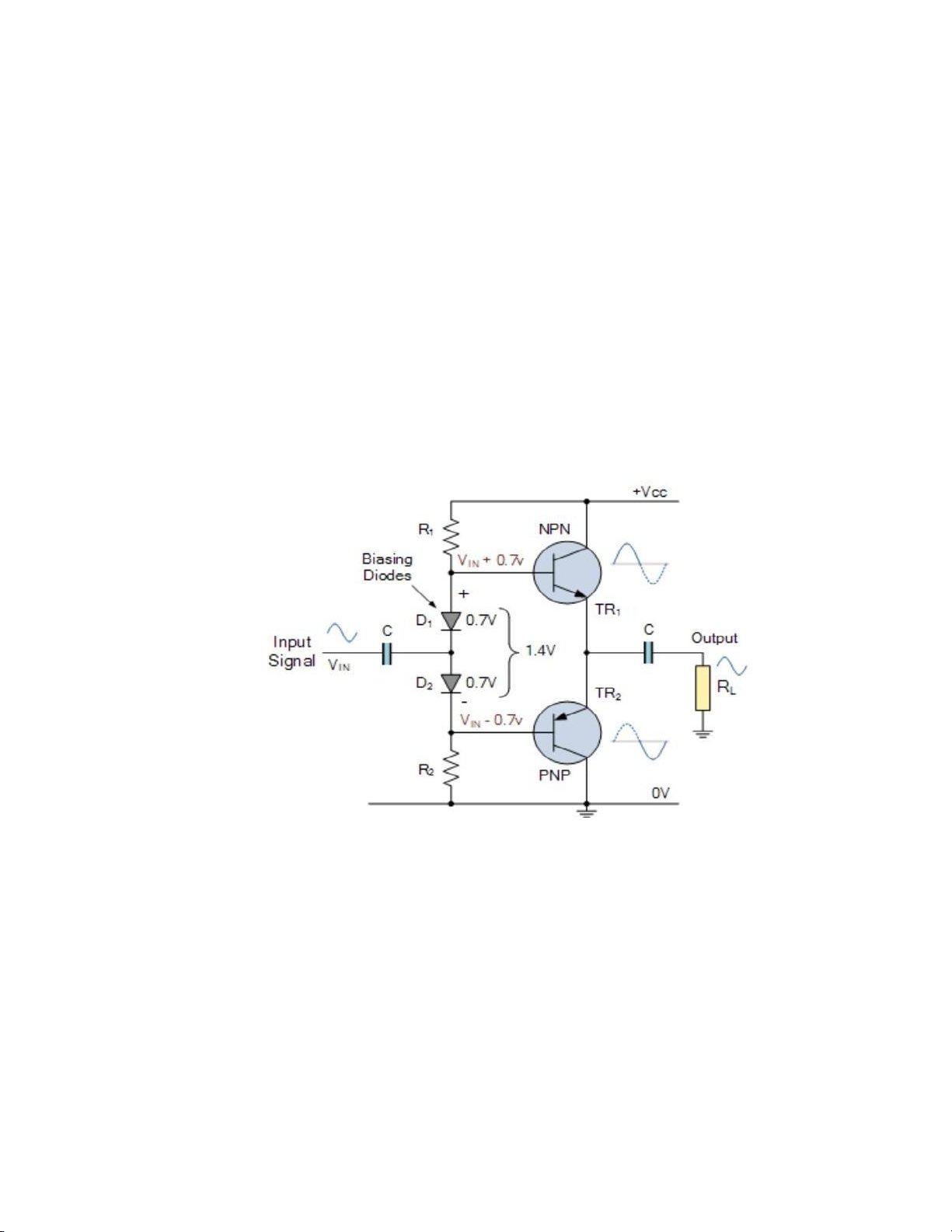
In our product, we use the class AB amplifier diode biasing because the use of
biasing resistors may not solve the temperature problem, one way to compensate for
any temperature related variation in the base-emitter voltage 𝑉𝐵𝐸 is to use a pair of
normal forward biased diodes within the amplifiers biasing arrangement as shown.
Fig1.11 Class AB Amplifier Diode Biasing
The biasing of a Class AB amplifier output stage is generally adjusted to suit a
particular amplifier application. The amplifiers quiescent current is adjusted to zero
to minimize power consumption, as in Class B operation, or adjusted for a very
small quiescent current to flow that minimizes crossover distortion producing a true Class AB amplifier operation
CHAPTER 2. DESIGN PRODUCT 2.1 Problem analysis
The technical requirements for this product are given:
• Input signal: Vin(rms)= 50mV AC • Power consumption: 2W
• The resistance of speaker/ the load: 8Ω
From the given specifications of the product, we have to design our product that can adapt all the requirements.
By first analyzing the requirements, we can calculate the output voltage:
V(rms)=Vout(p)=√2PRL = √2×2×8=4√2
To obtain the output voltage, make the music sound, we need to know how many times we
need to amplify our input signal. From what we have already know, we can calculate the voltage gain as follow: Av
To avoid signal to be cut off, Vcc >= 2Vout(rms) = 2.4√2=11.3 V Choose Vcc=12V 2.2Block diagram
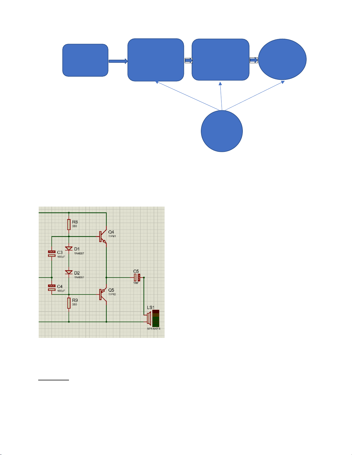
Our product is divided into 4 main parts: AC signal source, Power source, Amplifier and
Speaker or Load. In these parts, the Amplifier includes 2 blocks are Voltage amplifier and Power amplifier. AC signal Voltage Power source amplifier amplifier Speaker Power source 2.3Power amplifier Fig2.4 Power amplifier DC Mode
IL(p)= VL(p)/ RL = 4√2 / 8 Ω = 0.7A
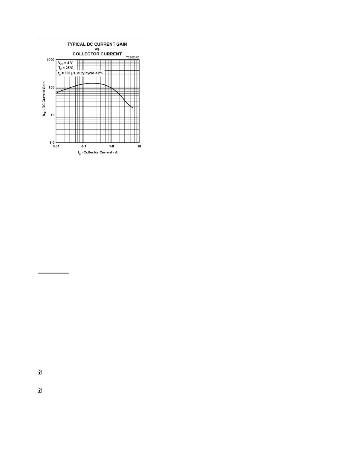
Figure: DC current gain of TIP41
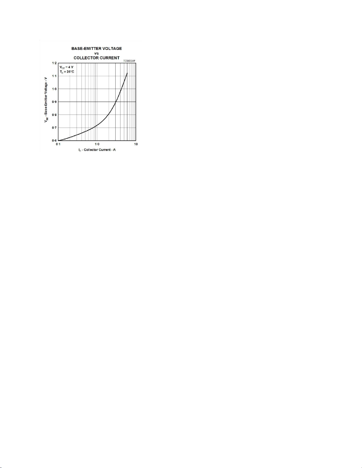
Assume βQ4 and βQ5 = 50 based on datasheets of TIP41 and TIP42.
IBQ4 = IBQ5 = IL(p) / βQ4 = 0.7 A / 50 = 14mA We know, Vcc - 0.7V - 0.7V = 10.6V VR8 = VR9 = 10.6V / 2 = 5.3V
R8 = R9 = VR8 / IBQ4 = 380 Ω AC Mode re3 = 26mV / IL(p) = 0.04 Ω
We have the input and output impedances of the power amplifier:
Zi3 = [RB//β (re3 // RL)] / 2 = 98(Ω) Zo3 = RE//re3 = 0.04 (Ω)
Ai3half = Av3 . Zi3half / RL= 1. (196) Ω /8 Ω = 24.5
Ii(c4) = Ii(c5) = IL(p) / Ai3 = 0.7 A/ 24.5 = 28.57 mA
Ii3(p)= Ii(c4) +Ii(c5) = 28.57 mA + 28.57mA = 57.14mA 2.4 Voltage amplifier
In the voltage amplifier circuit, we use the Common-Emitter voltage-divider bias
configuration. The voltage-divider bias configuration is less dependent on the change of
temperature and that’s why this kind of configuration has the good stability rather than other biasing configurations. 2.4.1 Stage 1 2.4.1.1 DC Mode
The audio amplifier circuit uses BJT type NPN: 2N2222. We chose it since it can be used
for low power amplification, also it is cheap and it fulfills our requirements. By using its
datasheet then we decide the current gain of this type of BJT. Data Sheet
We chose Q (VCEQ1; ICQ1) = (4.5 V; 1.5 mA)
By using the datasheet of 2N2222, we find out the current gain coincide with the Q-point: β=150
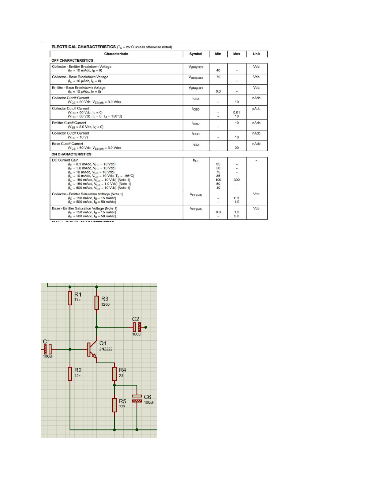
Fig2.1 The first stage
By using the theorem and the formula in Part 1.1 DC biasing- BJT’s theorem in the Chapter
1, we can calculate the resistors of the circuit in the stage 1. Vcc = VR3 + VR4+VR5+VCEQ1 =6V
Voltage divider bias has “temperature stabilization” by using 𝑅5, then tradeoff of the emitter resistor 𝑅5 is recommend:
𝑉𝑅𝐸 ~ 1/10 DC source and then,
Choose VR4 + VR5=>1.2V VR3=4.8 V
We know: 𝐼𝐶 ≈ 𝐼𝐸
R3=VR3/ ICQ1-> R3=3200(Ω)
We know, β (R4 + R5)>=10R2 -> So, Choose R2=12kΩ So, R1=71kΩ 2.4.1.2 AC Mode The voltage gain 𝐴𝑉: re1 = 26mV / ICQ1 = 17.33 Ω
Av1 = -R3/ (re1 + R4) = -80-> R4 = 22.67(Ω) => R4 = 23Ω
R4 + R5 = (VR4+VR5) / ICQ1= 800 Ω => R5 = 777Ω
By using the theorem on the BJT AC analysis’s theorem in the Chapter 1. We can calculate
the input impedance and output impedance:
The input impedance of a transistor with an unbypassed resistor 𝑅𝐸 is determined by Zi1
=R1 || R2 || βQ1 (re3 + R4) = 3806.52Ω Where, Zo1= R3 = 3200Ω Current of the input signal,
Iin(p) = Vin(p)/ Zi1 = 50√2mV / 3806.52Ω =18.6 µA
From above assumption we can calculate the maximum current gain,
Ai (max) = IL(P) / Iin(p) = 37674 2.5 Current amplifier
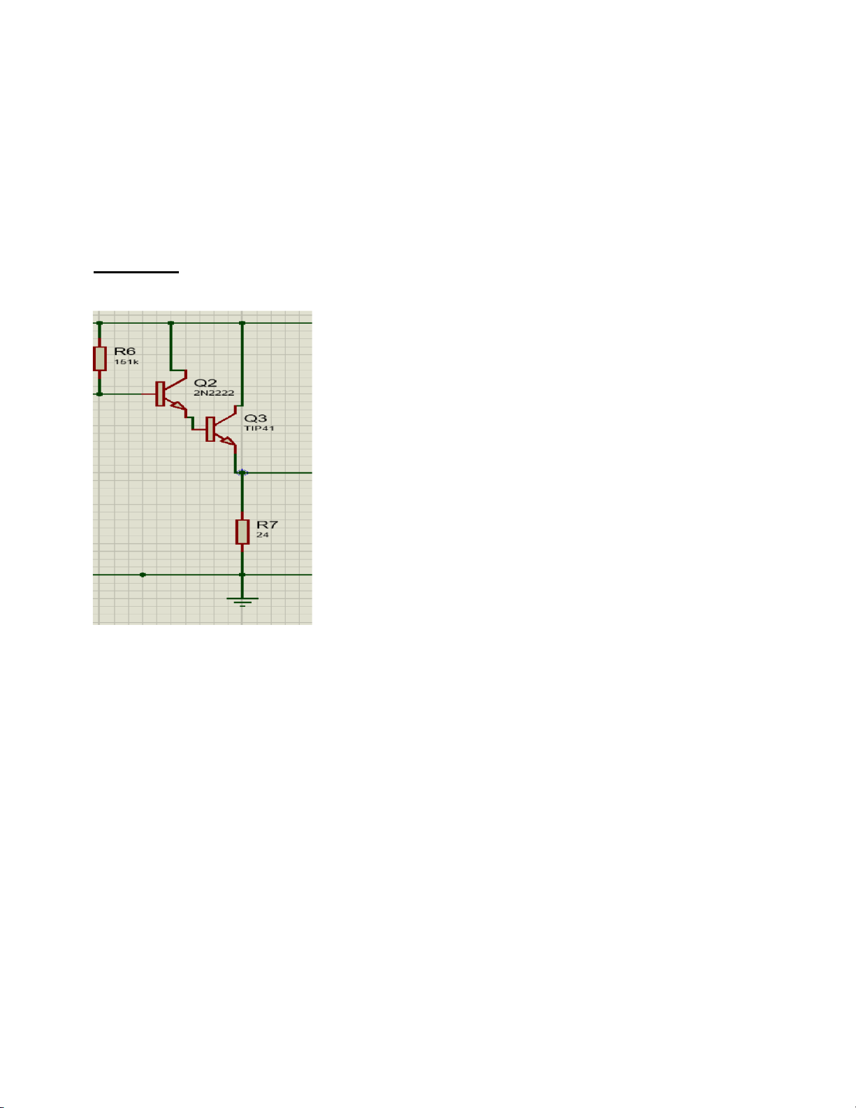
At the third stage, we choose Darlington transistor in Common-Collector (Emitter
Follower) to amplifier the current. At this configuration, the voltage gain is always approximately 1. DC mode:
Fig2.1 The first stage
Since 1 stage doesn’t amplify current much, we assume input current for 2 stage is same as the input current for stage1.
Ii2(p)= Iin(p) = 18.6 µA Current gain of stage 2 : Ai2 =Ii3(p) / Ii2(p) = 3072
Choose the Q (VCEQ3, ICQ3) = Q (6V, 0.25A)
The coefficient β of the Darlington transistor is 𝛽 = 𝛽Q2𝛽Q3 =190× 55
Fig: VBE Voltage characteristic of TIP41 At
the first transistor in Darlington:
IBQ3 = ICQ3 / 𝛽Q3 = 0.25A / 55 = 4.55 mA
ICQ2 ≈ IEQ2≈ IBQ3 = 4.55mA Assume VBEQ2 = 0.7V
IBQ2 = IEQ2 / (𝛽Q2 +1) = 30.1µA
R6 = (Vcc – VBEQ2-VBEQ2-VR7) /IBQ2 = (12 v- 0.7v-0.73v-6v)/ 30.1µA R6= 151kΩ R7 = VR7 / IR7 = 6V / 0.25A
Choose R7 = 24 Ω At AC Mode: The internal resistors, re2= 26mV/ IR7 = 0.1 Ω
Zi2 = R6|| 𝛽D (R7 // Zi3) =86.31k Ω Then, Zo2 = re2 = 0.1Ω
And the voltage gain at this kind of configuration is 𝐴𝑉3 (NL) ≈ 1
Tài liệu liên quan:
-
Báo cáo Thí nghiệm Mạch Điện Tử: Kiểm Chứng Mạch Op-Amp | Mạch điện tử | Đại học Bách Khoa Hà Nội
29 15 -

Bài giảng Chương 2: Mạch khuếch đại cộng hưởng môn Mạch điện tử | Đại học Bách Khoa Hà Nội
31 16 -

Câu hỏi trắc nghiệm Linh kiện điện tử | Đại học Bách Khoa Hà Nội
41 21 -
Đồ án Chi Tiết Máy (Cơ Khí) - Thiết Kế Hệ Thống Dẫn Động Băng Tải
78 39