Chapter 01: Intro to Integrated Circuits and Digital Systems | Môn Integrated Circuits and Systems Design - Đại học Sư phạm Kỹ thuật Thành phố Hồ Chí Minh
Chapter 01: Intro to Integrated Circuits and Digital Systems Môn Integrated Circuits and Systems Design. Tài liệu được sưu tầm gồm 116 trang, giúp bạn ôn tập tốt hơn. Mời các bạn đón xem.
Môn: Integrated Circuits and Systems Design (ICSD336764) 8 tài liệu
Trường: Trường Đại học Sư phạm Kỹ thuật Thành phố Hồ Chí Minh 4.4 K tài liệu
Tác giả:


Preview text:
lOMoAR cPSD| 58728417
Integrated Circuit and Digital system Design
Associate Professor. Truong Ngoc Son
Email: sontn@hcmute.edu.vn Mobile: 0931.085.929
Department of Computer and Communication Engineering
Faculty of Electrical and Electronics Engineering Tools lOMoAR cPSD| 58728417 ▪ Lecture notes ▪ Textbook ▪ Software ▪Xilinx ISE Design Suite
Truong Ngoc Son, Ph.D - Department of Computer and Communication Engineering lOMoAR cPSD| 58728417 Student activity Attending class
It is absolutely important that you attend class regularly (>80%) Solving the problem
Take all examinations ( including online exam, paper-based exams) Submit the homework on time
Truong Ngoc Son, Ph.D - Department of Computer and Communication Engineering lOMoAR cPSD| 58728417
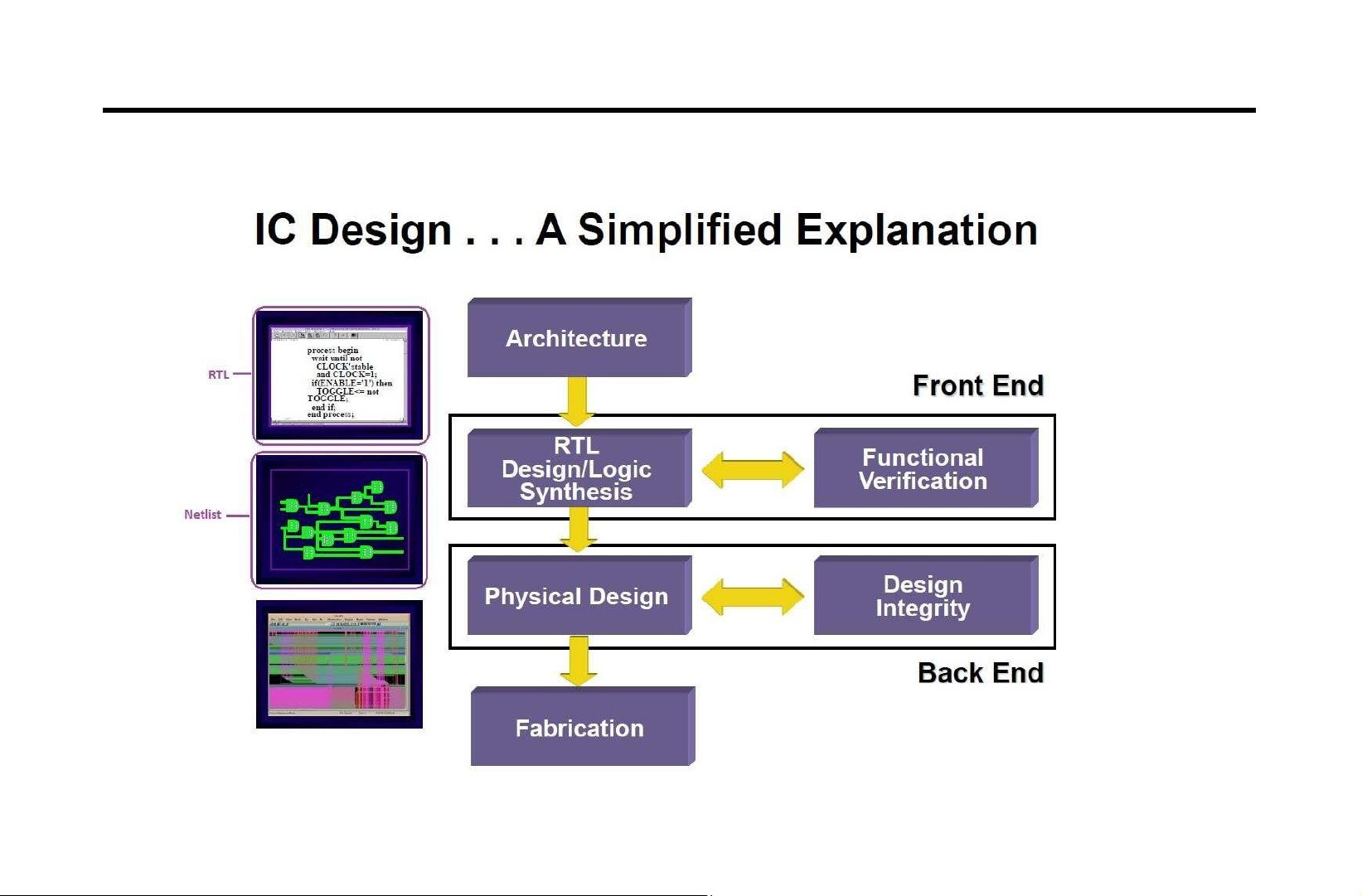
Integrated circuit Design ASIC FPGA lOMoAR cPSD| 58728417
Integrated circuit Design lOMoAR cPSD| 58728417
Integrated circuit Design lOMoAR cPSD| 58728417 Introduction
❑ How to go from Idea/Algorithm to the actual hardware module RippleCarryAdderII (Cin, X, Y, S,Cout); parameter n = 4; input Cin; input [n- 1:0] X, Y; output [n-1:0] S; wire [n-1:0] C; Full_Adder stage0
(Cin, X[0], Y[0], S[0], C[1]); Full_Adder stage1
(C[1], X[1], Y[1], S[1], C[2]); Full_Adder stage2
(C[2], X[2], Y[2], S[2], C[3]); Full_Adder stage3 (.Cout(Cout), .Cin(C[3]), .x(X[3]), .y(Y[3]), .S(S[3])); endmodule lOMoAR cPSD| 58728417 Introduction ASIC FPGA
❑ Hardware Description Language (HDL) :Verilog
❑ Professional Verilog Coding for Synthesis
❑ Verification Techniques ❑ FPGA Architectures ❑ Digital System Design with Xilinx FPGAs lOMoAR cPSD| 58728417 Introduction
❑ ASIC Digital Design Flow (from Verilog to the actual
Chip!) ❑ Synthesis Algorithms ❑ Power Dissipation ❑ Power Grid
and Clock Design ❑ Fixed-point Simulation Methodology
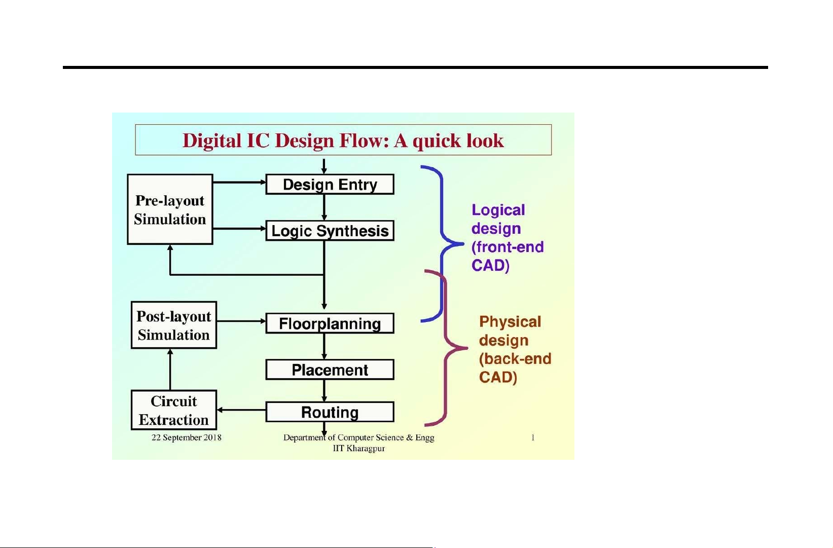
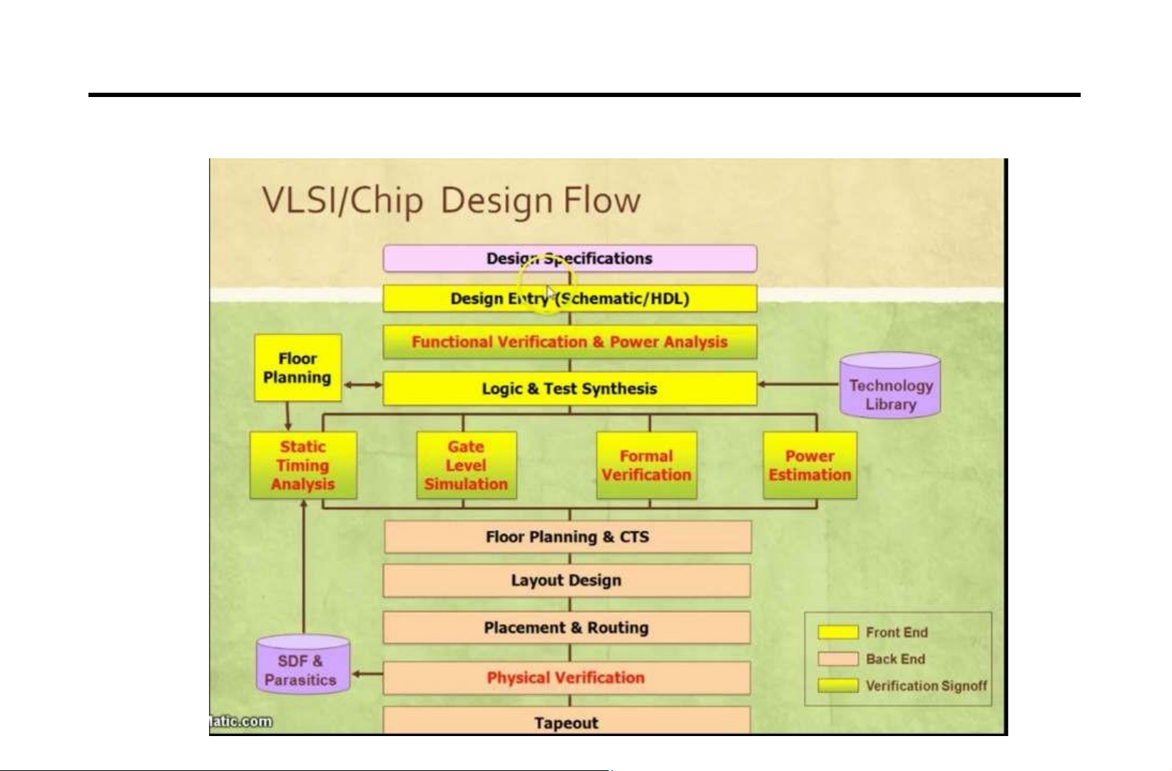
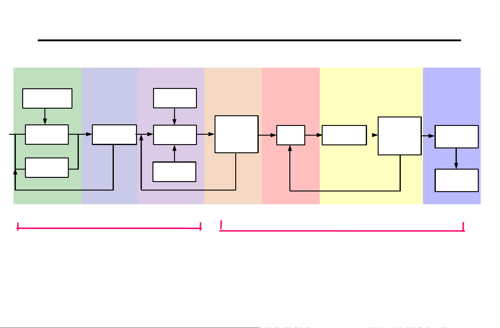
❑ Detailed Design Optimization Workshop with ISE (for the fist time!) lOMoAR cPSD| 58728417 Introduction Standard Specifications Cells Pre-Layout Post-Layout Simulation Yes Timin g Yes Back Yes RTLCoding Synthesis APR Tim ing Logic Pass ? Alanysis An nota tion Alanysis v erification Pass? Pass? NO TestBench Timing NO NO Constrain ts Tapeout 1 . 2 .Simulation 3 .Synthesis 4 . Placement &routing 5 . Timing Analysis HDLCodin &Verification Front-End Back-End
❑ In this course we learn all the above steps in detailfor ➢ ASIC Platform ➢ FPGA Platform lOMoAR cPSD| 58728417 Introduction:
❑ Hardware Description Language
➢Verilog Fundamentals ▪ Language Fundamentals
▪ Modeling Combinational/Sequential Logic Circuits ▪ Modeling Finite State Machines
➢Verilog for Verification
▪ Verification/Simulation techniques with test-benches
➢Verilog for synthesis
▪ Verilog Styles for Synthesis
▪ Architectural techniques for high-speed designs o Parallel proc., pipelining, retiming, … lOMoAR cPSD| 58728417 Introduction: ▪ Implementations of common operations o Complex multiplication,
division, complex norm, CORDIC
▪ Fundamentals of fixed-point realization
❑ PLDs & FPGA Architectures ➢FPGA Technologies
▪ SPLDs (PAL and PLA architectures)
▪ Commercial CPLD Architectures ▪ SRAM/LUT Based FPGAs ▪ Anti-fuse/MUX Based FPGAs ▪ Flash Based FPGAs ➢FPGA Architectures
▪ Heterogeneous/Homogeneous FPGAs
▪ Fine-grained, coarse-grained and platform FPGAs lOMoAR cPSD| 58728417 Introduction: ➢FPGA Elements
& Design Trade-offs
▪ Logic Cells Common Architectures
▪ Programmable Routing Channels Design
▪ I/O & Pad architectures ➢Commercial FPGAs ▪ Altera (FLEX 10K, Stratix III) , Xilinx (XC4000, Virtex II,4,5), Actel (Act3, Axcelerator)
❑ Advanced Digital System Design with Xilinx FPGAs ➢ Design Creation ➢ Synthesize ➢ Simulation lOMoAR cPSD| 58728417 Introduction: ➢ Constraints Entry ➢ Implementation
➢ Implementation Results Analysis – Timing Analysis
➢ Implementation Results Analysis – Power Analysis
➢ Implementation Results Improvement
➢ Device Configuration and Programming ➢ Design Debugging ❑ Core Generator ➢ CORE Generator Tool
➢ Intellectual Property (IP) Cores lOMoAR cPSD| 58728417 Introduction: ➢ CORE Generator Tool files ➢ Design Flows ➢ Defining
Memory Contents for RAM and ROM ➢ Defining
Coefficient Values in a COE File ❑ ASIC Design Flow:
➢HDL Coding & Verification ➢Synthesis
& Timing Optimization
▪ Complete Synopsys Design Complier Design Flow ➢Physical Design ▪ Cadence First Encounter lOMoAR cPSD| 58728417 Introduction:
▪ Floorplan (Initial floorplan and power planning) ▪ Placement
(Full-scale floorplan and clock tree insertion)
▪ Routing (power routing & Nanoroute) ▪ Timing Closure (Analysis & Optimization of setup and hold
time violations) ▪ Fill (Filler Cells, Metal Fill, and Verify Geometry)
❑ CAD Tool Algorithms:
➢Synthesis Algorithms ➢Two-level Optimization
➢Multi-level Logic Optimization ➢Technology Mapping lOMoAR cPSD| 58728417 Introduction: ❑ Power Dissipation ➢ Power Dissipation concept ➢ Dynamic Power ➢ Static Power ➢ Challenges lOMoAR cPSD| 58728417 Introduction:
❑ Power Grid and Clock Design ➢ Power Distribution Design ▪ Introduction ▪ IR Drop ▪ Ldi/dt Drop ➢ Decoupling Capacitances ➢ Clock Considerations ➢ PLL/DLL Architecture ❑ Prerequisites: ➢Only Digital Logic! lOMoAR cPSD| 58728417 Introduction:
➢All the skills you need will be taught in the course ❑ Softwares you will learn: ➢Altera Quartus ➢Xilinx ISE ➢Mentor Graphics Modelsim ➢TCL Scripting ➢Synopsys Design Compiler ➢Cadence SOC Encounter
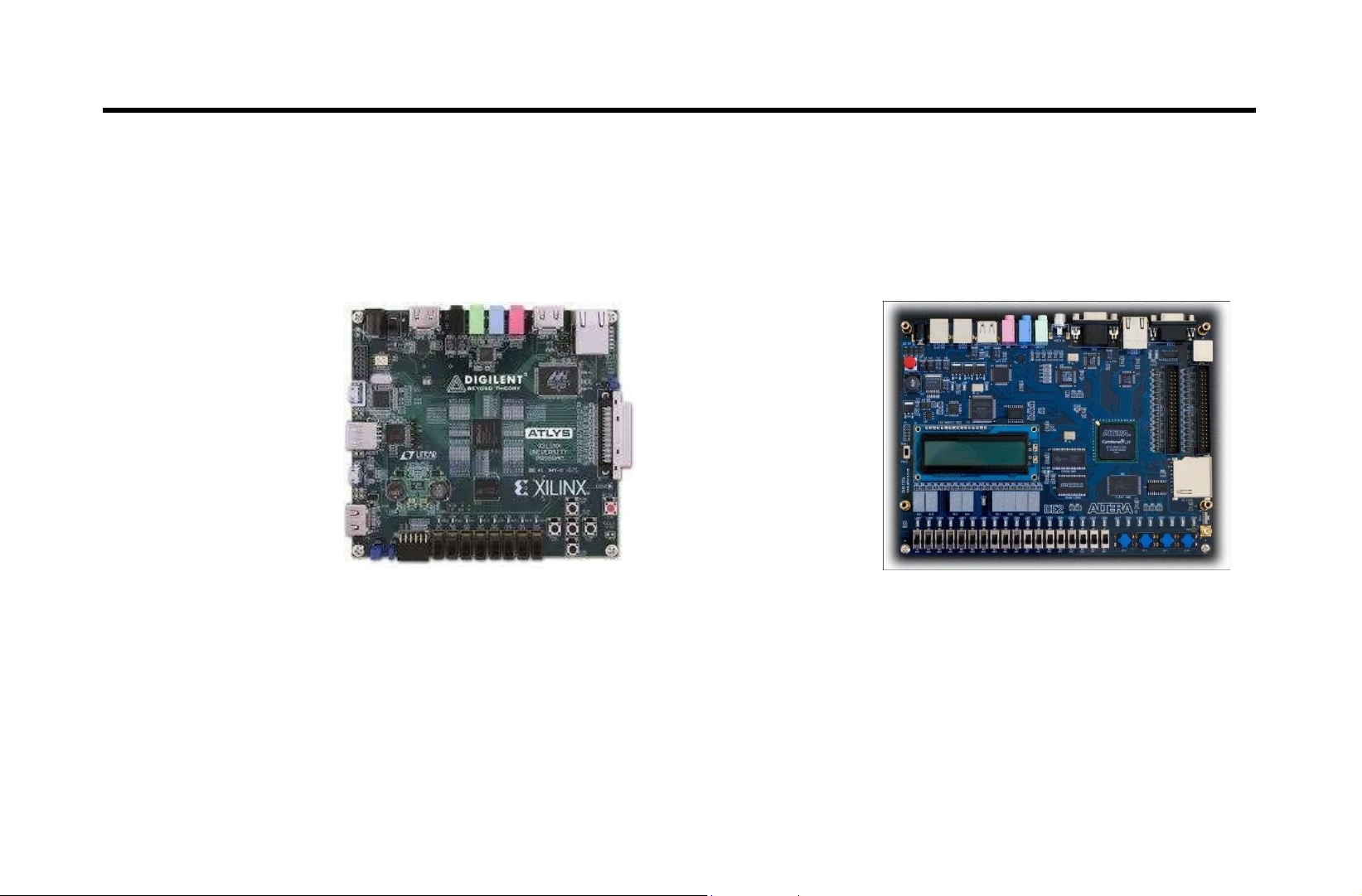
❑ Implementation Platform: lOMoAR cPSD| 58728417 Introduction: ➢Altera DE2 Board ➢Atlys Xilinx Board
❑You will do several practical assignments including Verilog Coding,
Tài liệu liên quan:
-

Báo cáo Thực tập Thiết kế Mạch Tích hợp VLSI | Môn Integrated Circuits and Systems Design - Đại học Sư phạm Kỹ thuật Thành phố Hồ Chí Minh
201 101 -
Báo cáo cuối kỳ | Môn Integrated Circuits and Systems Design - Đại học Sư phạm Kỹ thuật Thành phố Hồ Chí Minh
115 58 -

Tìm hiểu giao tiếp SPI | Môn Integrated Circuits and Systems Design - Đại học Sư phạm Kỹ thuật Thành phố Hồ Chí Minh
163 82 -

Integrated Circuits and Systems Design Lab | Môn Integrated Circuits and Systems Design - Đại học Sư phạm Kỹ thuật Thành phố Hồ Chí Minh
100 50