Chapter 5: Tech layout design rules môn VLSI | Trường Đại học Bách Khoa Hà Nội
Any circuit physical mask layout must conform to a set of geometric constraints or rules called as ëLayout Design rulesí before it can be manufactured using particular process. Tài liệu được sưu tầm gồm 29 trang, giúp các bạn nắm vững kiến thức, rèn luyện kỹ năng và đạt được kết quả tốt trong học tập. Mời các bạn đón xem!
Môn: VLSI 7 tài liệu
Trường: Đại học Bách Khoa Hà Nội 5.8 K tài liệu
Tác giả:


Preview text:
lOMoAR cPSD| 59703641 CHAPTER 5: Layout Design Rules Introduction ◼
Any circuit physical mask layout must conform to a set of geometric
constraints or rules called as Layout Design rules before it can be
manufactured using particular process. ◼
The rules specify minimum allowable line widths for physical
objects on-chip such as Metal & PolySi interconnects or diffusion
areas, feature dimension and so on. ◼ For example: 1.
If metal line width is too small, it is possible for the line to break
during fabrication process and result of open circuits 2.
If the lines are places too closed to each other, it may form an
unwanted short circuit by merging during or after fabrication process
◼ Main objective of Layout design Rules is to achieve, for any circuit
to be manufactured with a particular process, a high overall yield
and reliability while using the smallest possible silicon area.
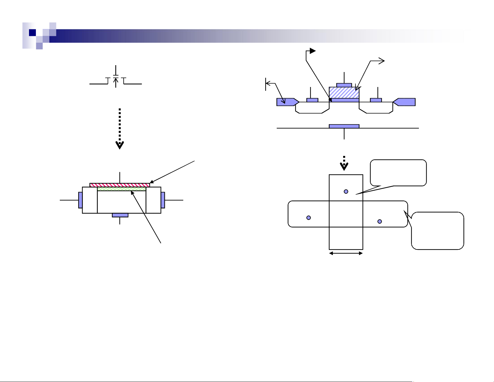
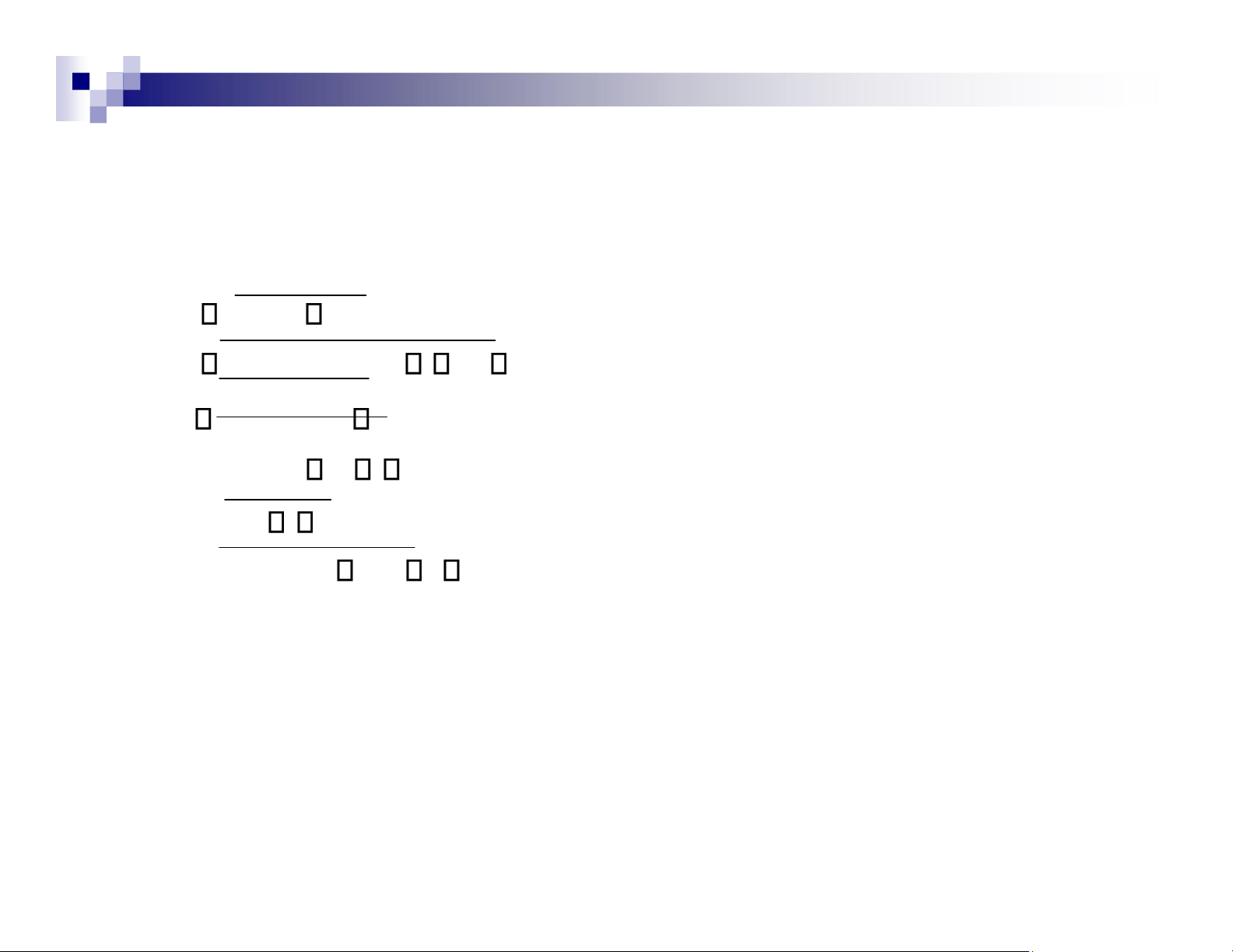
Simple NMOS Transistor Layout lOMoAR cPSD| 59703641 G Thin Oxide G PolySi S D Thick Oxide S D SUB N N P-Substrate SUB G Silicon PolySi Mask Oxide G S n p D n Insulator S D Active SUB Area Mask Field Induced N-channel Gate Length lOMoAR cPSD| 59703641
Simple NMOS Transistor Layout
◼ Active area mask defines the extent of Thick Oxide ◼ Polysilicon
mask also controls the extent of Thin Oxide (@ Gate Oxide)
◼ N-type implant has no extra mask:
→ It is blocked by thick oxide & polysilicon → The implants is self-
aligned ◼ Substrate connection is to the bottom of wafer → All substrates is to ground NMOS Transistor
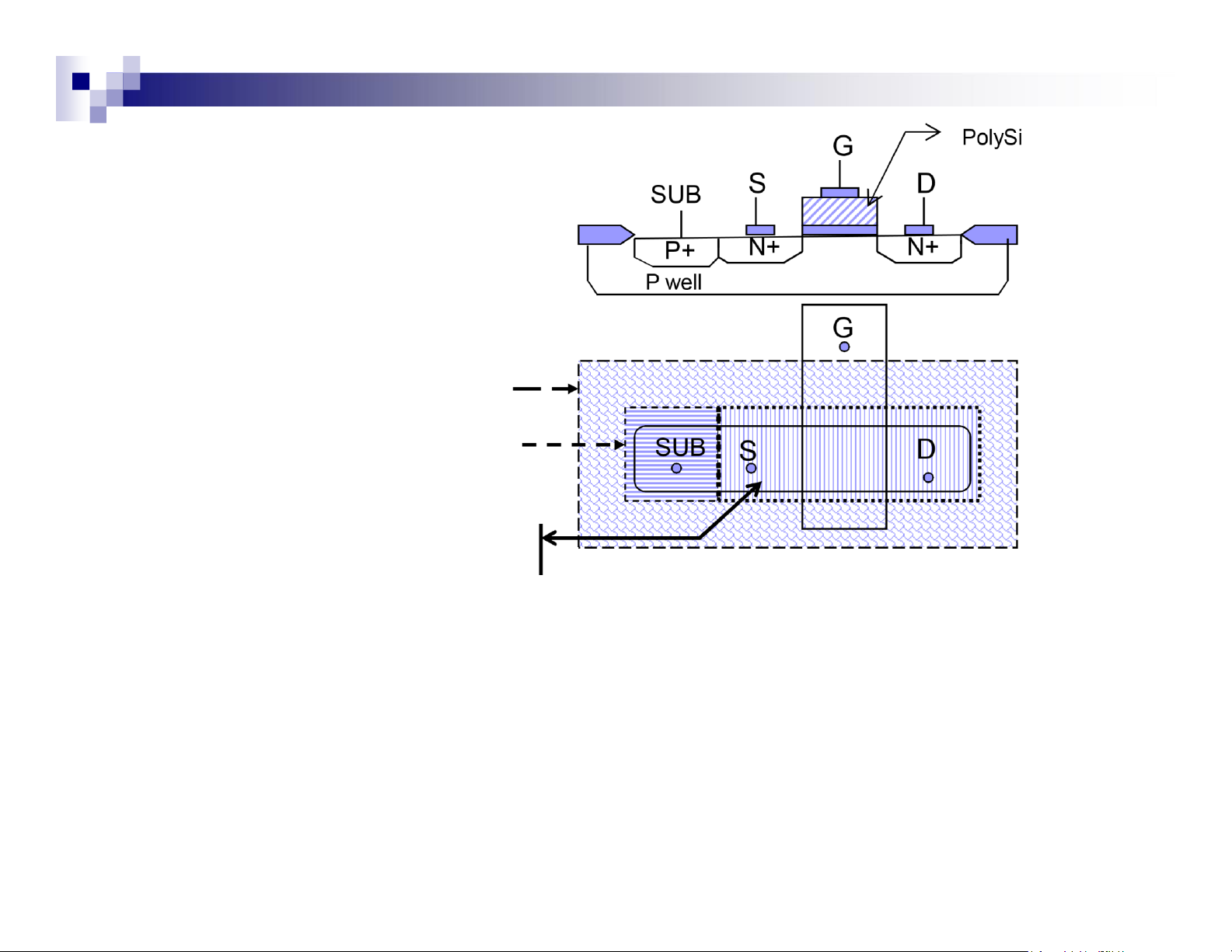
Where it is not suitable for substrate connections to be shared, a more complex process is used.
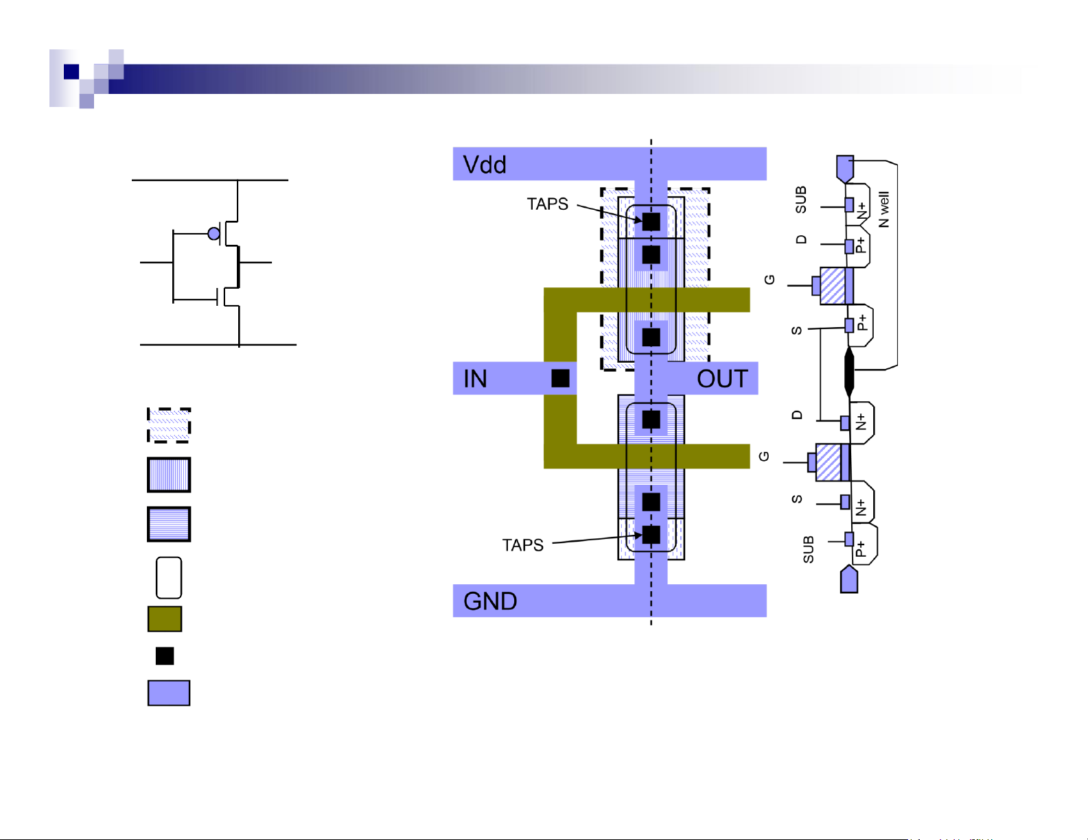
◼ Five Masks must be used to define the transistor: 1. P well For Isolation 2. Active Area 3. PolySilicon 4. N+ Implant 5. P+ Implant lOMoAR cPSD| 59703641 P well Mask P+ Implant Mask N+ Implant Mask lOMoAR cPSD| 59703641 CMOS Inverter Vdd Output Input Gnd N well P implant N implant Active Area PolySi Contact Window Metal TAPS Substrate Connection lOMoAR cPSD| 59703641 CMOS Inverter
◼ The process describe here is an N well process since it has only an N well
◼ P well & Twin Tub processes also exist
◼ Note that the P-N junction between chip substrate and N well will remain reverse biased / 0 V
◼ Thus, the transistors remain isolated
◼ N implant defines NMOS source/drain and PMOS substrate contact
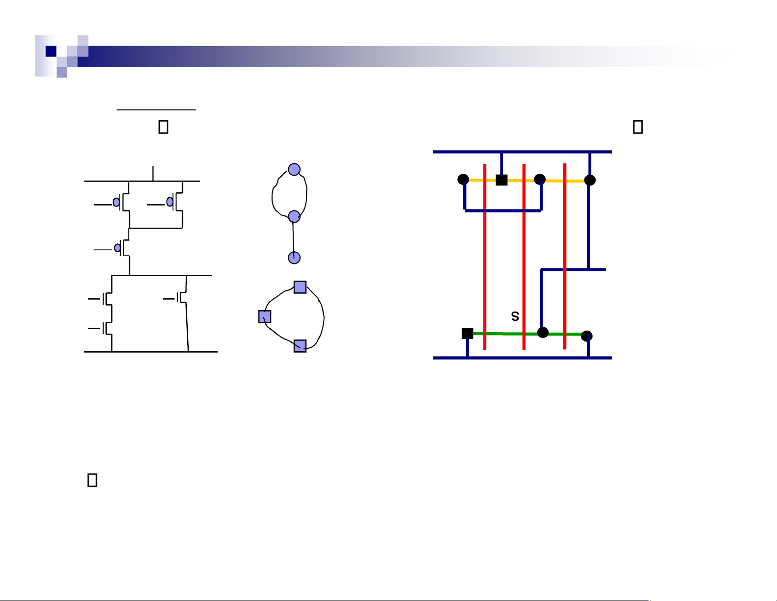
◼ P implant defines PMOS source/drain and NMOS substrate contact Stick Diagram
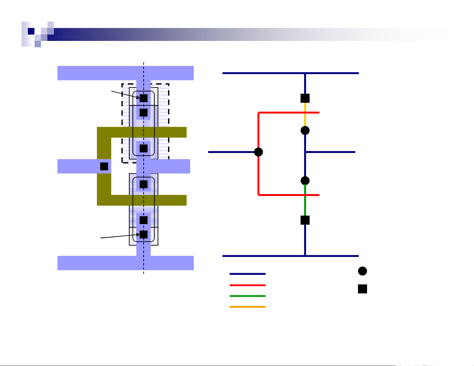
◼ Explore your design space since it can give: → Implications of crossovers → Numbers of contacts
→ Arrangement of devices & connections ◼ Process Independent
layout but Technology dependent
◼ Easy to expand to a full layout for a particular process:
→ Magic (symbolic editor) → Tanner tools lOMoAR cPSD| 59703641
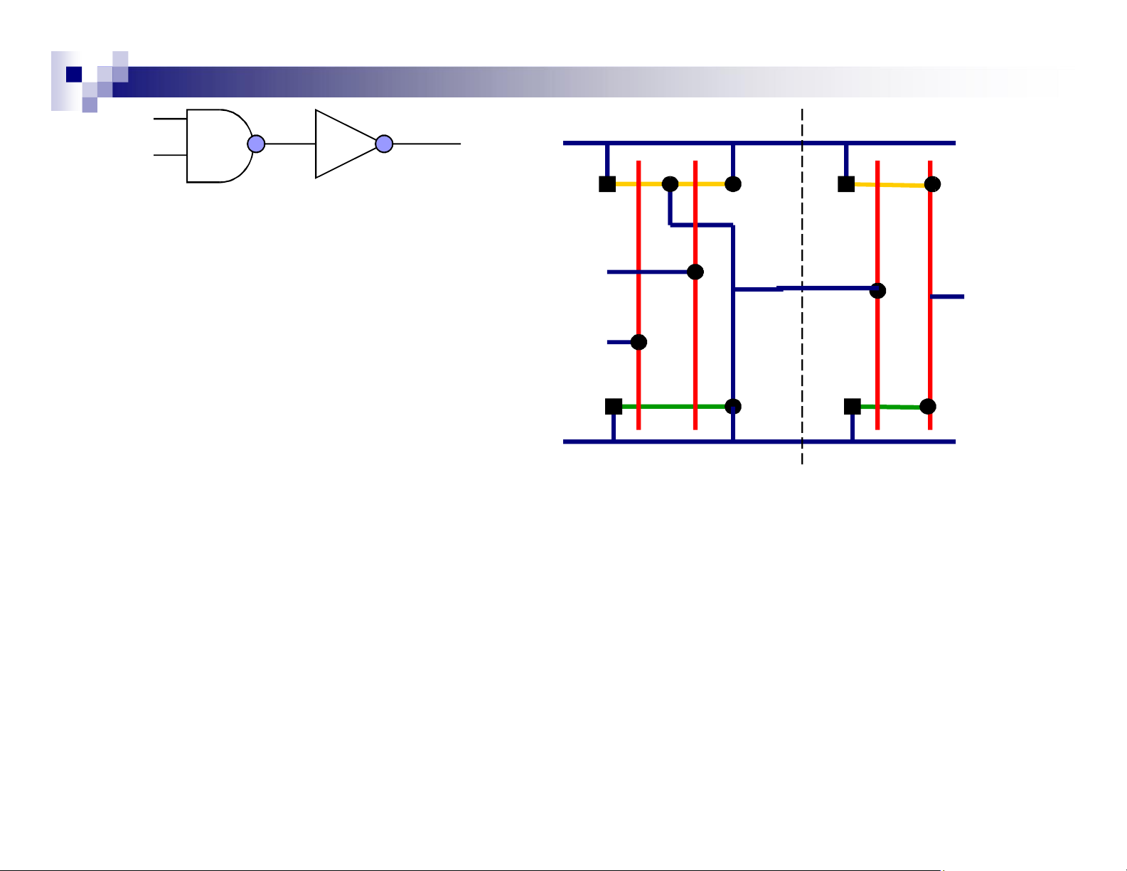
Stick Diagram of CMOS Inverter Vdd TAPS IN OUT TAPS GND Metal (Blue) Contact Polysilicon (Red) N+ (Green) Combined P+ (Yellow) contact + Taps lOMoAR cPSD| 59703641 Stick Diagram of NAND Gate Vdd A Out B GND
▪ Note that different style of layout will affect the overall
performance of the device such as silicon area, timing, parasitic effect and so on
▪ Thus, careful selection of layout style is crucial and must be carefully taken care
▪ Exercise: Draw the stick diagram of AND, OR, NOR, EX-OR lOMoAR cPSD| 59703641 Complex Logic Gates Layout ▪
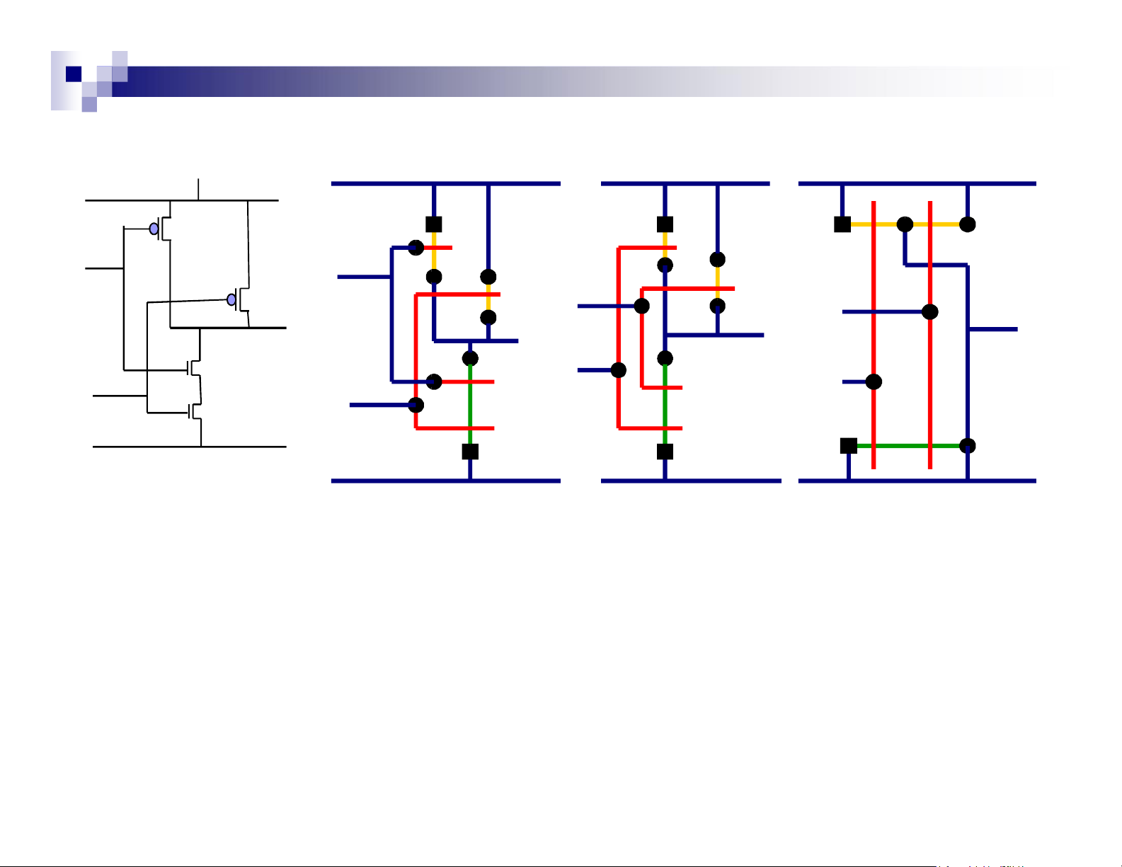
For complex Logic gates, all complementary gates may be
designed using a single row of n-transistors above or below a
single row of p-transistors, aligned at common gate connections ▪ Thus, in this layout style:
1. The gates are designed using unbroken row of transistors in which
abutting source-drain connections are made
2. This called as line of diffusion rule, since the transistors form a line of
diffusion intersected by polysilicon gate connections. lOMoAR cPSD| 59703641 Vdd Vdd G G Line of diffusion s D s D A B Out Out A B s D D Line of diffusion GND GND Complex Logic Gates Layout Vdd
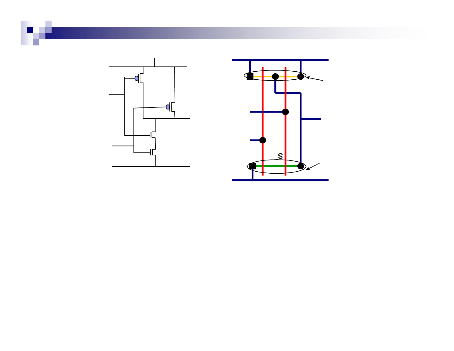
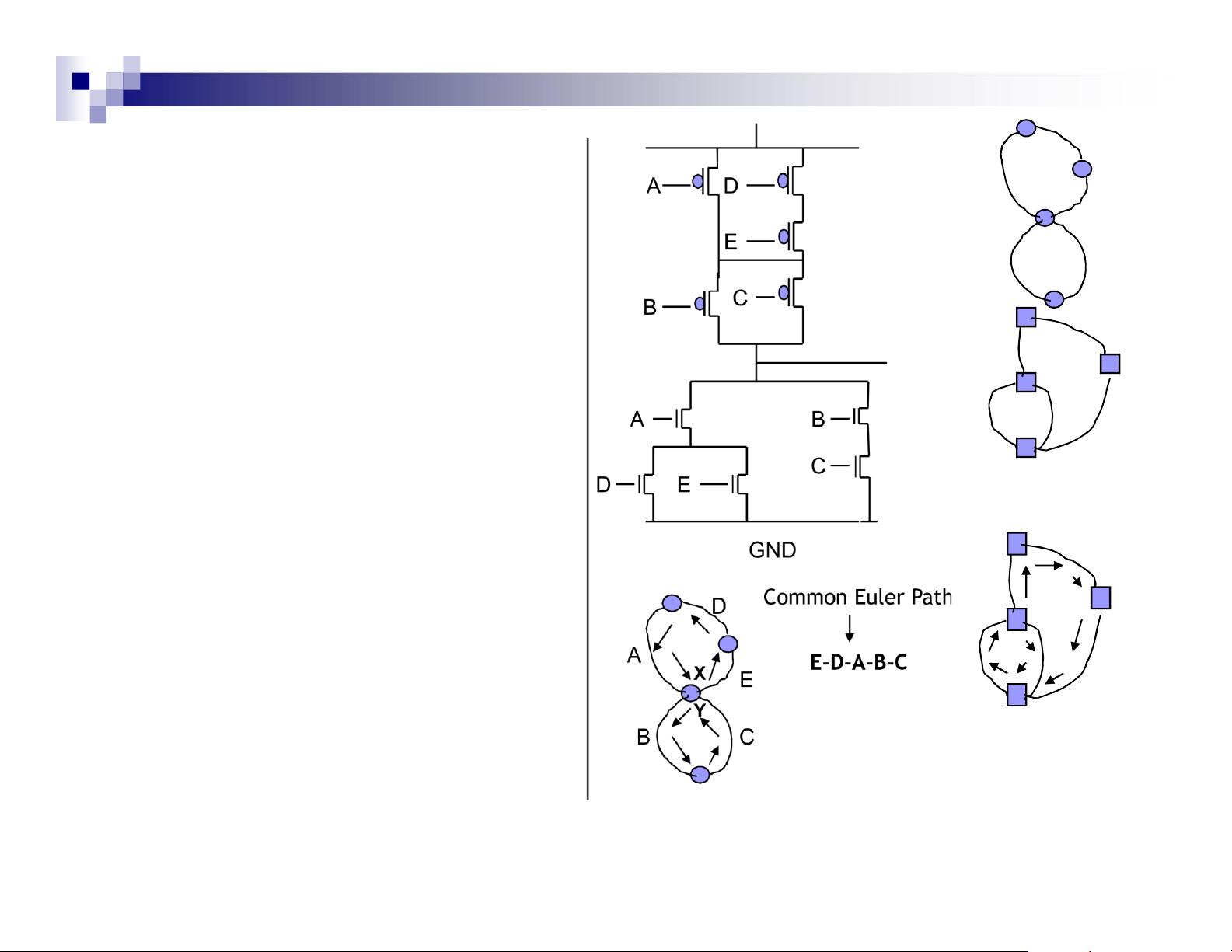
◼ However in this layout style, the gate arrangement must be find first by : lOMoAR cPSD| 59703641 D 1. Careful selection of transistorA orderingE 2. Careful orientation of transistorBC source and drain B ◼ Method use for finding A optimum gate
ordering /orientation called as E C Euler Out p-network graph
Path where all complex circuits B is: A
1. First converted to Euler path of X pnetwork and n-network graph E C 2. Then find the common Euler Y path forD both graph ◼
The Euler path is defined as an uninterrupted path that lOMoAR cPSD| 59703641
transversen-network graph each edge (branch) of the graph exactly once only. ◼ Example :
1. Draw the CMOS logic gate of the Boolean function of: D
Z A D E( ) BC Complex Logic Gates Layout lOMoAR cPSD| 59703641 E D A B C Vdd s D s D S s s D D D A D E C B B C Out A Out D E A B C D E D S D S D D S D S GND GND Vdd Z AD E BC ( ) lOMoAR cPSD| 59703641 Finding An Euler Path
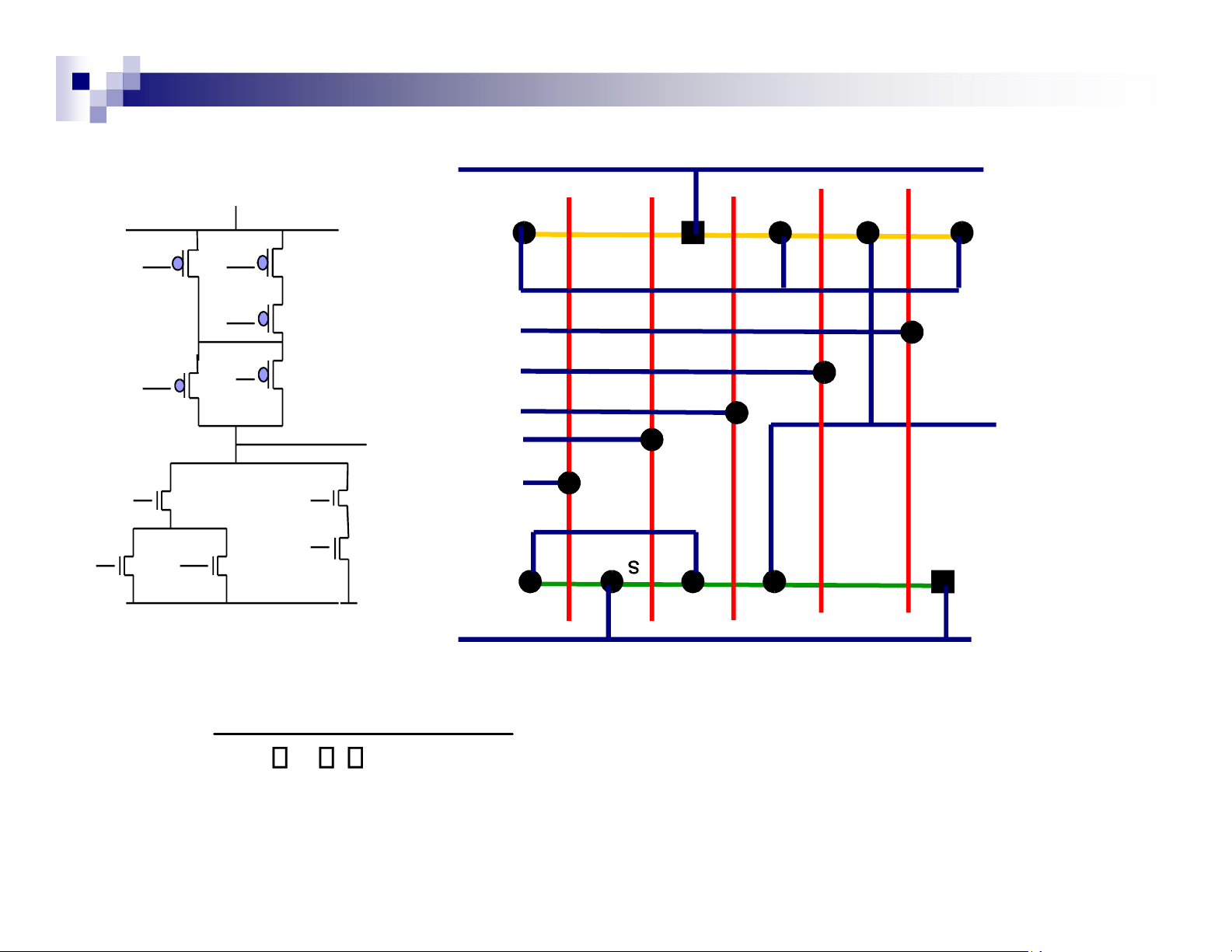
◼ Exercise: Sketch the CMOS logic circuits, CMOS logic symbol, find
the Euler Path & Sketch the Stick Diagram of the following Boolean Function:
1. Z (AC ) B
2. Z ( A B C D E F )( )
3. F ((AB CD) ( )) 4. F A B C D (( ) 5. F A BC ( ) 6. F ABC DE F ( ) ( ) lOMoAR cPSD| 59703641 Finding An Euler Path Z AC B ( ) Vdd C A B Vdd D A S C S D s D A C B B ZZ A A B C B D D s D s C GND GND
a. Logic Circuitsc. p & n network graph d. Stick Diagram A The common Euler lOMoAR cPSD| 59703641 Path is C-A-B C Z Note that the circuit has many common EP B since it is a simple cct b. Logic Symbol Multiple Gates
◼ Objective is to understand the method of making a layout of a system
that consist of multiple gates Example: lOMoAR cPSD| 59703641 Gates can be abutted to create more complex functions
Gates should all be of same height
- Power & Ground rails will then line up The output of one gate can be
routed directly to the input of the next
Note that this view is somewhat
very simplistic but as inter-gate connections are usually more complex Multiple Gates
◼ All gate inputs and outputs are available at the top and bottom of
the cells in polysilicon: → Routing of circuits is much easier → All routing is external to cells. lOMoAR cPSD| 59703641
- Thus, we can change inside of the cells without destroying circuit
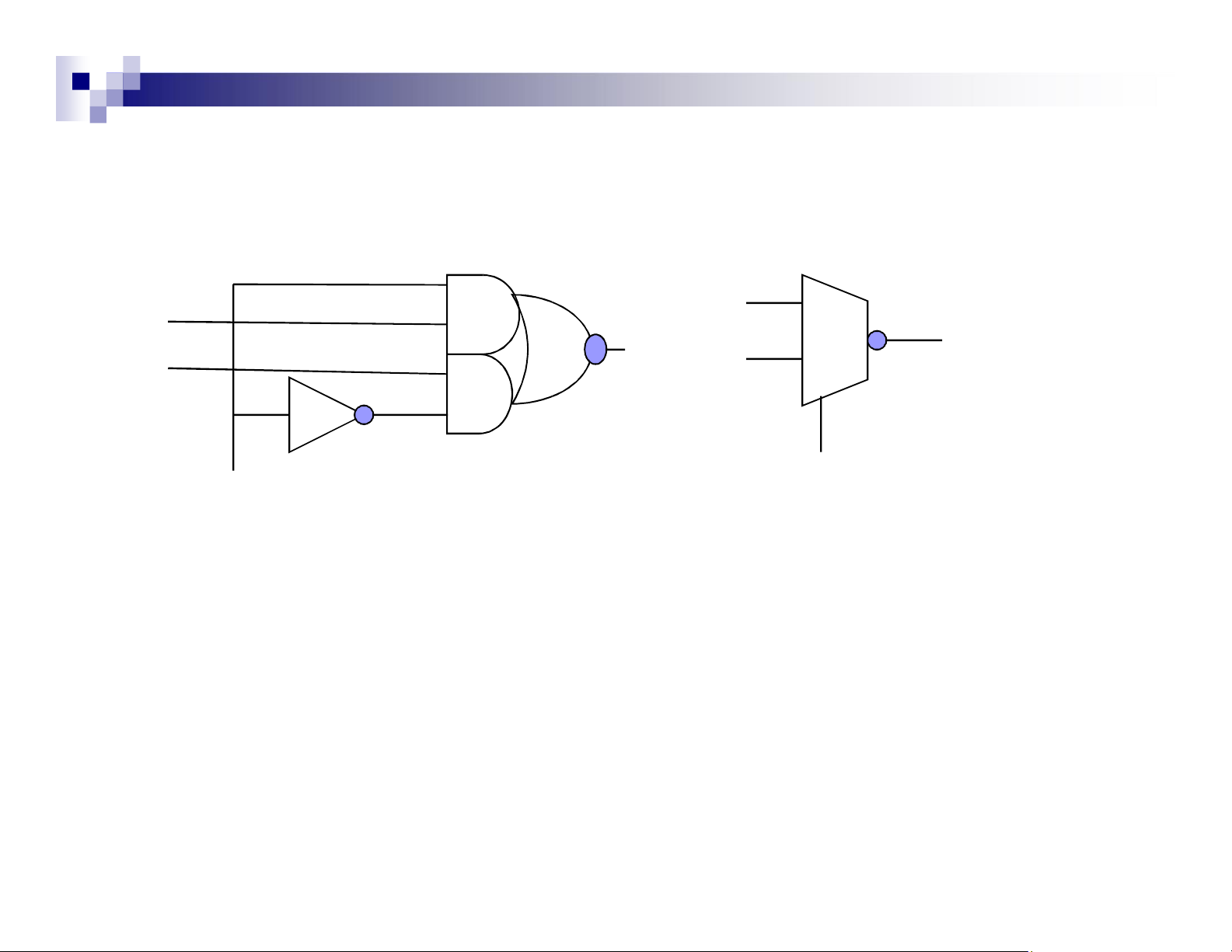
Exercise: Make the layout of the multiple gates below A BF S Multiplexer Multi-cell Layout
◼ Objective is to explain a logical approach of implementing multi-cell layout
◼ All multi-cell layout consists of two stages:
→ Placement → Routing ◼ We have designed our cells with a
constant height and with inputs and outputs at the top and bottom of
the cell. Thus, we have the beginnings of a logical approach to multi- lOMoAR cPSD| 59703641
cell layout ◼ Placement : Cells are placed in one or several equal
length with inter-digitized power and ground rails Multi-cell Layout
◼ Two conductor routing: In the channels between the cells, we route
metal horizontally and polysilicon vertically
◼ This logical approach means that we should never have to worry about signals crossing
◼ This make life considerably easier for a computer (or even a human) to complete the routing
◼ We must only ensure that the two signals will not meet in the same
horizontal or vertical channel
◼ For most VLSI applications we have two layer metal processes.
◼ The norm is to use only metal for inter-cell routing and either Metal1
horizontally (for power rails) and metal2 vertically (for inputs and outputs) or vice versa. LAYOUT USING TANNER ◼
Objective :To introduce the method of using CAD tools for making
gates Layout i.e Tanner (L-edit, S-edit & T- Edit) lOMoAR cPSD| 59703641 ◼
S-Edit : is a powerful Schematic entry package, which can
generate netlist directly usable in T-Spice simulations ◼
T-Edit : performs fast and accurate simulation of analog and mixed
analog/digital circuits. The simulator can analyze large, complex
designs with hundreds of thousands of circuit elements. ◼
L-Edit: layout tool that represents the masks that are used to
fabricate an integrated circuit. In L-Edit, layers are associated with
masks used in the fabrication process. Different layers can be
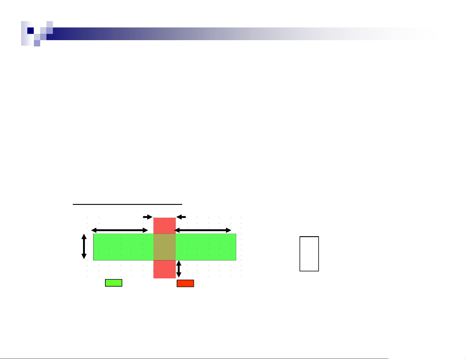
conveniently represented by different colors and patterns. LAYOUT USING TANNER ◼ CMOS Inverter Step 1: Draw NMOS side first Rule 3.1: min 2 l 5.5 Rule 3.4: min 3 l l Rule 2.1: min 3 l 2 Wn = 5 l = 5u l Rule 3.3: min 2 l A c t i v e P o l y
Tài liệu liên quan:
-
Hướng dẫn sử dụng Cadence trong thiết kế IC số môn VLSI | Trường Đại học Bách Khoa Hà Nội
162 81 -
Bài tập thực hành - Thiết kế bộ đếm nhị phân & LFSR môn VLSI | Trường Đại học Bách Khoa Hà Nội
96 48 -

Báo cáo Thiết kế Synchronous FIFO với RAM từ RTL đến GDS môn VLSI | Trường Đại học Bách Khoa Hà Nội
113 57 -

Bài tập lớn Thiết kế đồng hồ số môn VLSI | Trường Đại học Bách Khoa Hà Nội
131 66