Đề cương môn Tiếng anh chuyên ngành- Trường Đại học bách khoa - Đại học đà nẵng.
ChipletTechnology:RevolutionizingSemiconductorDesign-AReview
Đề cương môn Tiếng anh chuyên ngành- Trường Đại học bách khoa - Đại học đà nẵng.
Tài liệu gồm 7 trang , giúp bạn tham khảo, ôn tập và đạt kết quả cao
Môn: Tiếng anh chuyên ngành (BKDN) 19 tài liệu
Trường: Trường Đại học Bách khoa, Đại học Đà Nẵng 1.7 K tài liệu
Tác giả:


Preview text:
See discussions, stats, and author profiles for this publication at: https://www.researchgate.net/publication/378156097
Chiplet Technology: Revolutionizing Semiconductor Design-A Review
Article in Saudi Journal of Engineering and Technology · February 2024
DOI: 10.36348/sjet.2024.v09i02.006 CITATIONS READS 0 1,632 1 author: Vivek Gujar IndoAI Technologies P Ltd
28 PUBLICATIONS 17 CITATIONS SEE PROFILE
Al content fol owing this page was uploaded by Vivek Gujar on 13 February 2024.
The user has requested enhancement of the downloaded file.
Saudi Journal of Engineering and Technology
Abbreviated Key Title: Saudi J Eng Technol
ISSN 2415-6272 (Print) | ISSN 2415-6264 (Online)
Scholars Middle East Publishers, Dubai, United Arab Emirates
Journal homepage: https://saudijournals.com Review Article
Chiplet Technology: Revolutionizing Semiconductor Design- A Review Vivek Gujar1*
1Director, IndoAI Technologies Pvt. Ltd.
DOI: 10.36348/sjet.2024.v09i02.006
| Received: 02.01.2024 | Accepted: 09.02.2024 | Published: 12.02.2024
*Corresponding author: Vivek Gujar
Director, IndoAI Technologies Pvt. Ltd. Abstract
This article explores the transformative journey of semiconductor design from monolithic structures to the cutting-edge era
of chiplets. Chiplets, modular components offering specific functionalities, have emerged as a catalyst, reshaping the global
semiconductor industry. Their capacity for tight interconnectivity, diverse applications, and cost-effective manufacturing
marks a paradigm shift. The article delves into the historical context of Moore's Law, the rise of chiplets, and their impact
on the semiconductor landscape. It further discusses key considerations in chiplet architecture, optimization algorithms,
and future adoption in industries like data centers, mobile devices, AI, and automotive. Chiplet-based designs promise
enhanced efficiency, collaboration, and innovation, heralding a new era in semiconductor evolution.
Keywords: Chiplets architecture, complex-function, manufacturing costs.
Copyright © 2024 The Author(s): This is an open-access article distributed under the terms of the Creative Commons Attribution 4.0 International
License (CC BY-NC 4.0) which permits unrestricted use, distribution, and reproduction in any medium for non-commercial use provided the original
author and source are credited. 1. INTRODUCTION
complete system-on-a-chip (SoC) or a more complex
The technological evolution in semiconductor
semiconductor device. Chiplet technology creates
design has witnessed a paradigm shift from traditional
smaller, specialized chiplets that can be interconnected
monolithic chip architectures to the innovative era of
to form a larger, more powerful chip. These chiplets can
chiplets. Initially, single-chip designs were predominant,
be manufactured separately and assembled onto a
but the limitations posed by size constraints and substrate or package [2].
manufacturing costs led to the emergence of chiplets. These modular components, featuring specific
Chiplets, or small chips, can be the size of a
functionalities, enable a more flexible and scalable
grain of sand or bigger than a thumbnail and are brought
approach. Chiplets optimize performance, reduce costs,
together in a process called advanced packaging [3]. The
and facilitate customization by combining multiple
idea behind chiplets is to break apart the system on a chip
smaller chips into a cohesive system. This evolution
into its composite functional blocks, or parts. Sub-
represents a transformative trend, shaping the future of
elements of a complex-function chip could be made as
semiconductor design, fostering collaboration, and
chiplets, where these sub-elements might include
unleashing new possibilities in diverse industries, from
separate computational processor or graphics unit, an AI computing to IoT and beyond.
accelerator, an I/O function, or a host of other chip
functions [4]. Chiplets are individual semiconductor
In a rapidly evolving technological landscape
components or microchips that are manufactured and
and its advancements, the advent of chiplets has become
designed for specific tasks and are integrated into a larger a transformative force, reshaping the global
circuit [5]. Chiplets, essentially are small semiconductors
semiconductor industry, Chiplets, with their capacity to
integrated into robust systems, have redefined the
integrate small semiconductors into robust systems, have
conventional norms of semiconductor design and
revolutionized the semiconductor landscape. chiplets
manufacturing. Their capacity for tight interconnectivity
have emerged as a catalyst, reshaping the global
has not only propelled performance to new heights but semiconductor industry [1].
has also introduced a cost-effective paradigm to chip
manufacturing. The ability to tightly interconnect Chiplets are individual semiconductor
chiplets boosts performance and offers a cost-effective
components that can be integrated together to form a
approach to chip manufacturing. Bonding chiplets
Citation: Vivek Gujar (2024). Chiplet Technology: Revolutionizing Semiconductor Design- A Review. Saudi J Eng 69 Technol, 9(2): 69-74.
Vivek Gujar; Saudi J Eng Technol, Feb, 2024; 9(2): 69-74
tightly together can help make more powerful systems
For instance, the Intel 4004 chip in 1971, with 2,250
without shrinking the transistor size [3].
transistors and a 10,000nm process, exemplified the
doubling trend. Subsequently, the 1974 Intel 8080 chip,
The technology of ongoing race to reduce
featuring 6,000 transistors and a 6,000nm process on a
transistor sizes, the global chip industry has increasingly
20mm2 chip, continued this trajectory. This remarkable
embraced in recent years as chip manufacturing costs
trend persisted until the early 2020s, with the exponential
soar in the race to make transistors so small they are now
increase in transistor count contributing to the
measured in the number of atoms. The tightly bonded
continuous enhancement of computer performance [6].
assembly of chiplets is a pivotal strategy for achieving
However, challenges emerge as the industry approaches
more powerful systems without further reducing the size
physical limits and encounters economic constraints in
of individual transistors. This has become particularly
maintaining Moore's Law as Moore’s Law shows signs
crucial as the semiconductor landscape experiences a
of slowdown since 2000. The gap between predictions of
seismic shift in response to the escalating demand for
Moore’s Law and the actual performance of chips grew
more potent and energy-efficient electronic devices. In a
by 15 times by 2008. Dennard scaling began to slow
panel discussion at CadenceLIVE Europe, experts from
down significantly in 2007 and nearly lapsed in 2012 [7,
academia and industry converged to address the
8]. Despite these challenges, the enduring legacy of
limitations posed by Moore's Law and traditional 2D
Moore's Law has significantly shaped the trajectory of chip architectures.
technological advancement, marking a pivotal era in the
history of microchip evolution [6].
As the industry grapples with these challenges,
the promises of 3D-IC chiplet integration have gained
3. Modularity of Chiplets & Design
prominence. Chiplets, through decades of industry
The modularity of chiplets, a revolutionary exploration, have evolved into indispensable
concept in semiconductor design, allows for the creation
components that offer a flexible and efficient solution for
of highly customized systems by combining smaller,
various compute subsystems. The potential to
specialized components. This modular approach
revolutionize the semiconductor industry became
enhances flexibility, promotes cost-effectiveness, and
evident as chiplets opened doors to a whole new level of facilitates the seamless integration of diverse
soft IP reuse, steering away from the monolithic design
functionalities, ushering in a new era of adaptable and
philosophy that encapsulates everything onto a single
efficient semiconductor architectures. chip.
The inherent modularity of chiplets not only
This evolution of monolithic design creates
optimizes system performance but also offers scalability
unprecedented opportunities for catering to dedicated
and ease of upgrades. By breaking down traditional
needs in analog, radio frequency (RF), compute, and monolithic designs, chiplets enable targeted
power domains. The modular nature of chiplets allows
enhancements in specific areas like processing power,
for the customization of semiconductor systems,
memory, or specialized functions. This flexibility fosters
optimizing performance for specific functions. Thus, innovation, cost-efficient manufacturing, and
chiplet technology has become a cornerstone in
adaptability to evolving technological demands, marking
overcoming the limitations of traditional semiconductor
a paradigm shift in semiconductor engineering.
designs, ushering in a new era of flexibility, efficiency,
and innovation in the global semiconductor landscape.
Due to Moore framework, chiplet-based design
As the industry continues to explore and refine chiplet
technology addresses multiple challenges. Firstly, it
technologies, the future holds promising prospects for
integrates modular chips into a single package,
further advancements in semiconductor design and
efficiently solving scale, development cost, and period manufacturing.
issues. Secondly, advanced packaging technologies like
2.5D and 3D enable high-performance multi-chip
2. Background and Evolution interconnection, enhancing system integration,
In 1965, Gordon Moore, the Co-founder of
performance, and power optimization. Lastly, modular
Intel, made a groundbreaking prediction that has since
integration accelerates development speed, lowers costs,
become widely recognized as Moore's Law. This
and reduces thresholds, shifting the focus of chip
prediction posited that every two years, the number of
research and development towards core technologies and
transistors on a microchip would double at the same
algorithms, significantly boosting overall innovation
manufacturing cost per silicon area. The implication was
capabilities [8]. Chiplets improve the optimization
a consistent acceleration in the power and capabilities of
potentials on performance and power consumption by
computers, accompanied by a steady reduction in costs
recombining multiple small chips. Thus, it supports the
for consumers. Gordon Moore's foresight held true for
domain-specific customization and mitigating the effect
several decades, earning Moore's Law recognition as one
from the slowdown of Moore’s law for developing
of the most influential guiding principles in modern diverse chips.
innovation. Over the years, this prediction materialized
as demonstrated by the evolution of Intel's microchips.
© 2024 | Published by Scholars Middle East Publishers, Dubai, United Arab Emirates 70
Vivek Gujar; Saudi J Eng Technol, Feb, 2024; 9(2): 69-74
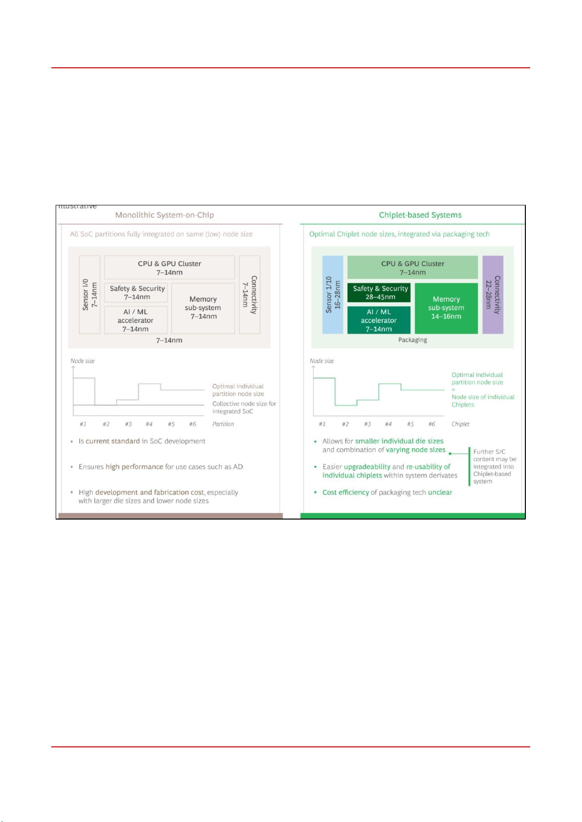
3.1 Chiplet Architecture and Design:
Chiplet Systems revolutionize System-on-Chip
Compute performance has been increasing
(SoC) design by dividing it into smaller units, or
exponentially in the past three decades. For
Chiplets, rather than consolidating all partitions on a
supercomputer, there has been 1.25 years per 2x
single die. Leveraging advanced packaging technologies
performance increase in the past 30 years. For personal
like 2.5D packaging, this modular approach enhances
devices, there has been 2.2~3 years per 2x performance flexibility, performance, and scalability in
increase in the past 15 years. Computing performance
semiconductor design, marking a significant departure
boost synchs with transistor count has been increasing.
from traditional monolithic structures [15]. Exhibit 1.
The available power consumption (power wall) limits
Chiplet Systems as an Alternative Alongside Monolithic
computing performance. Energy efficiency improvement SoC [15].
drives computing performance boost [9].
In chiplet design, critical considerations center
communication consumption and system temperature.
around seamless interconnectivity, efficient power
By introducing communication and temperature-based
distribution, and effective thermal management.
heuristic information, a balance is achieved using the
Interconnectivity is pivotal for the cohesive functioning
weight factor and algorithm, the peak temperature
of modular chips within a system, influencing
reduced by 8.34 K, and communication power
performance and data transfer. Effective power
consumption dropped by 232.13uJ compared to the
distribution ensures that each chiplet receives the
initial layout. This flexibility makes their algorithm
required power, optimizing energy usage. Thermal
adaptable to varying design requirements, offering
management is crucial to prevent overheating, as densely efficient control over the trade-off between
packed chiplets can generate substantial heat. Ensuring a
communication power consumption and temperature
balanced thermal environment enhances reliability and optimization. longevity. The synergy of these key design
considerations is imperative, guaranteeing the successful
Graening et al., 800mm2 design study seems to
implementation of chiplet technology, fostering optimal
indicate that the best size for chiplets is somewhere
performance, energy efficiency, and reliability in
between 50mm2 and 150mm2 for microprocessor logic semiconductor systems [10].
and above 200mm2 for random logic they examined the
case of a large design that could be built as a single
Wang et al., [9] present a multi-objective
monolithic system on chip (SoC) or as a system of
optimization algorithm that simultaneously optimizes
chiplets and show that optimal chiplet size depends on a
© 2024 | Published by Scholars Middle East Publishers, Dubai, United Arab Emirates 71
Vivek Gujar; Saudi J Eng Technol, Feb, 2024; 9(2): 69-74
wide range of parameters. Their analysis indicates that
approach. However, due to restrictions such as the
the smallest chiplet sizes that are viable cost-wise
maximum reticle area, cost, and manufacturing yield, the
depends both on technology node and on type of logic.
chip’s area cannot be continuously increased, and it
The optimal point appears to be 50-150mm2 in 40nm and
encounters what is known as the “area-wall”. In their
40-80mm2 in 7nm for microprocessor type logic [11].
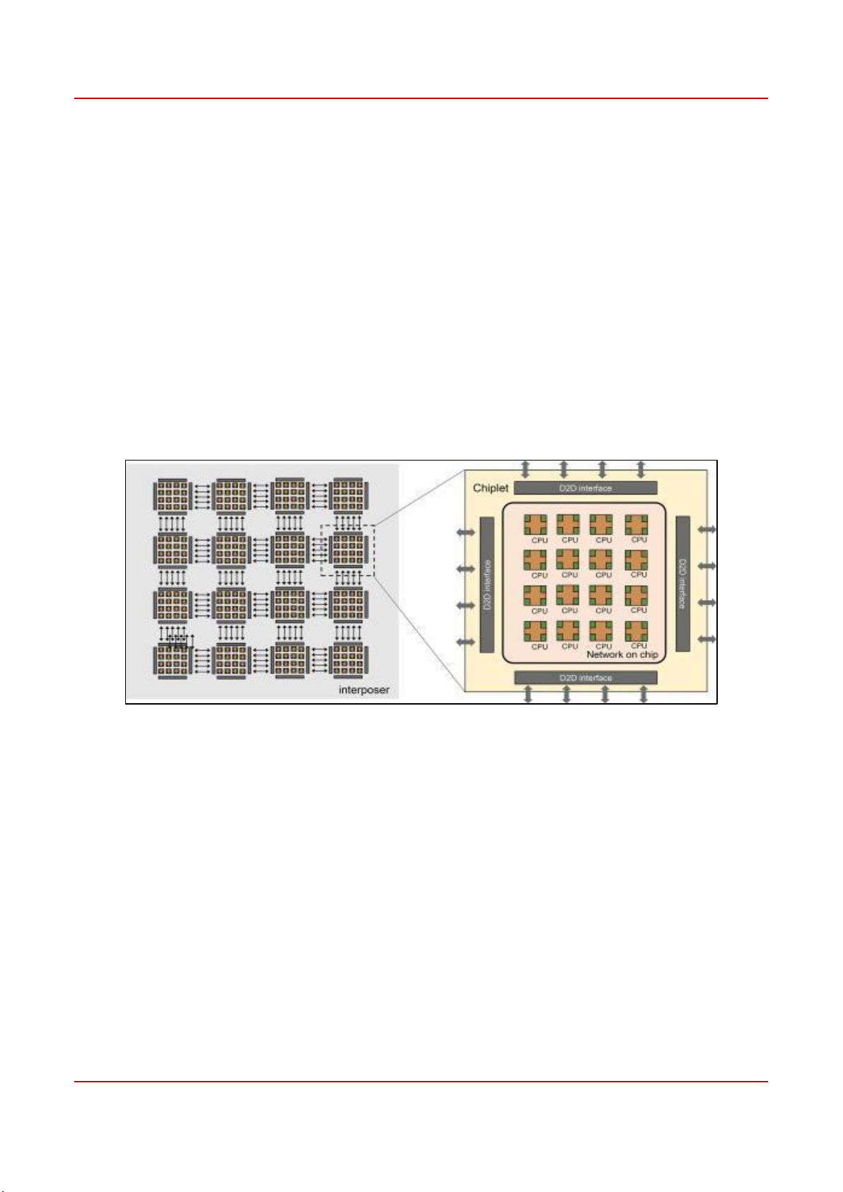
paper Yinhe Han et al., [13] provided a detailed analysis
of the area-wall and propose a practical solution, the Big
For Zhen et al., [12] multi-package architecture
Chip, as a novel chip form to continuously improve
was a popular alternative to optimize the reliability and
performance. The Zhejiang Big Chip adopts a scalable
cost for advanced packages to overcome the primary
tile-based architecture, as illustrated in fig below. This
challenge of the multi-package co-design problem,
processor consists of 16 chiplets, and it has the potential
which is the tradeoff between interconnection cost and
to scale up to 100 chiplets. In each chiplet, there are 16
reliability. Therefore, a co-design methodology was
CPU processors that are connected via a network-on-
adopted to optimize multiple packages simultaneously to
chip (NOC), and each tile is fully symmetrically
improve the quality of the whole system. To tackle this
interconnected to enable communication among multiple
challenge, they adopted mathematical programming
chiplets. The CPU processors are designed based on the
methods in the multi-package co-design problem
RISC-V instruction set. Moreover, this processor adopts
regarding the nature of the synergistic optimization of
a unified memory system, which means any core on any multiple packages.
tile can directly access the memory across the entire processor.
To improve performance, increasing the chip
area to integrate more transistors has become an essential
Zhuoping Yang et al., [14] first discussed the
encapsulated Intel's evolution, emphasizing that it was
diversity and evolving demands of different AI
no longer a one-size-fits-all company.
workloads and how chiplet brings better cost efficiency
and shorter time to market. The authors also discussed
4. Future Chiplet Adoption in Industry & Advantages
about heterogeneous chiplet architecture which is
Chiplet development is still emerging, but it
favored to keep scaling up and scaling out the system as
promises to transform the semiconductor industry and
well as to reduce the design complexity and the cost
electronics. Here's a peek into the potential future:
stemming from the traditional monolithic chip design.
Diverse Specialized Chiplets: Expect more chiplets tailored for specific functions, seamlessly
In the proceedings of ISSCC 2009 [20], Intel
combining different capabilities. This will lead to
presented a series of papers focusing on the Nehalem
highly efficient systems for tasks like edge
processor. The plenary session, led by Mark Bohr,
computing and scientific research.
underscored Intel's significant investment in advancing
Edge Computing and IoT: Chiplets are ideal for
system-on-chip (SoC) technology. This commitment
making IoT devices more power-efficient and
was evident in the design of the Core i7 Nehalem, which
responsive. In edge computing, chiplets enable real-
featured the integration of memory controllers and
time data processing, fueling smart cities,
DDR3 I/Os onto a shared substrate with the CPU cores.
autonomous vehicles, and intelligent infrastructure.
Notably, Intel signaled a strategic shift during this
Quantum Computing: Chiplets could revolutionize
period, expressing a vision that extended beyond the
quantum computing by offering accessible and
traditional PC market, particularly emphasizing interest
scalable solutions. Quantum chiplets, assembling
in dynamic sectors such as mobile technology. Bohr
quantum processors, may enhance performance and
reliability, pushing the boundaries of computation.
© 2024 | Published by Scholars Middle East Publishers, Dubai, United Arab Emirates 72
Vivek Gujar; Saudi J Eng Technol, Feb, 2024; 9(2): 69-74
As chiplet technology evolves [19], it is 3. Increased Yield:
expected to see chiplets being further utilized in some of
Smaller chiplet sizes enhance wafer utilization.
the following industries prominently.
Minimizes manufacturing defects, ensuring a
Data Centers: Chiplets are revolutionizing higher yield.
data center architectures by enabling efficient
and modular designs. They offer enhanced 4. Cost Efficiency:
performance and energy efficiency while
Enables cost savings by combining dies from
simplifying upgrades and maintenance. different nodes.
Mobile Devices: In smartphones and tablets,
Reduces over-specification and improves
chiplets can be customized to optimize power purpose-specific fits.
consumption, graphics, and AI processing,
resulting in improved performance and longer 5. Performance Optimization: battery life.
Task-specific chiplets deliver performance
AI and Machine Learning: Chiplet-based AI enhancements.
accelerators can be tailored for specific AI
Integrated photonics in multi-die packages offer
workloads, delivering faster inferencing and superior bandwidth density. training capabilities.
Automotive: Chiplets can enhance 6. Expanded Chip Area:
autonomous vehicles' processing power and
Overcomes size limitations imposed by reticle safety. size.
Allows for larger chip areas compared to
Chiplet architectures are fundamental to the monolithic designs.
continued economic viable growth of power efficiency
of AI, 5G and edge computing [21]. Due to the platform 7. Lower Power Consumption:
idea, the chiplet approach also allows scaling of Reduces interconnection distance and
computing power. If more power is needed to process AI minimizes power loss.
algorithms, then several of these circuits can be installed
Contributes to lower power requirements in on the chiplet system [22]. chiplet configurations.
Chiplet-based designs promise robust growth, driven by
following several key advantages [16, 17]:
8. Flexibility in Development:
1. Enhance Chip Production Efficiency:
Chiplet modularity facilitates swift adjustments
Independent manufacturing of chip modules. to product portfolios.
Utilizes diverse processes and latest
Enables design reuse and de-risks system-on- manufacturing technologies. chip development.
Elevates production efficiency and cost-
Shortens design time, promoting flexibility and effectiveness. adaptability.
Mitigates entire chip scrappage, enhancing reliability
Chiplets can provide many benefits in the
context of processor design in a post Moore’s Law world,
2. Facilitate Industrial Collaboration and Innovation:
but effective utilization of chiplets still requires careful
Fosters collaboration across diverse industries.
engineering and optimization along many different and
Enables different manufacturers to develop chip
sometimes conflicting dimensions [18]. modules.
In nutshell, the accelerated growth in the
Strengthens cooperative ties, accelerating
advanced packaging market, driven by chiplet innovation.
technology, presents a substantial opportunity for
Introduces a diverse array of product choices to
companies agile enough to embrace and leverage these the market. advancements. Annexure/s
Different Types of Chiplets for Computation Types of Chiplets Description Compute Chiplets
Primary processing units with CPU and GPU cores for executing computational tasks. Memory Chiplets
Dedicated memory modules like DRAM or HBM enhancing data access speeds and storage capacities. I/O Chiplets
Interfaces enable communication between chiplets, the external world, and peripherals. Fabric Chiplets
Facilitating high-speed data transfer and communication between chiplets within a package. Ref: Cadence
© 2024 | Published by Scholars Middle East Publishers, Dubai, United Arab Emirates 73
Vivek Gujar; Saudi J Eng Technol, Feb, 2024; 9(2): 69-74 CONCLUSION
5. https://chipedge.com/power-of-chiplets-in-the-
Over the past several years, chiplets have semiconductor-industry/
moved from a buzzword to a proven technology,
6. https://www.kandou.com/glasswing/2023-09-18-
enabling chip shipments in the millions of units per year.
history-of-the-chiplet-and-why-it-is-the-future/
7. https://fastercapital.com/content/The-Future-of-
Lacking a mature ecosystem, however, chiplet-based
Computing--Moore-s-Law-s-Lasting-Impact-and-
design has been available to only large vendors. Now, the Beyond.html
industry is poised for broader adoption once D2D
8. Li, T., Hou, J., Yan, J., Liu, R., Yang, H., & Sun, Z.
interfaces are standardized and a wave of vendors adopt (2020). Chiplet heterogeneous integration
new chiplet-based business models. Customer demand is
technology—Status and challenges. Electronics, 9(4),
creating momentum behind this approach, with the
670. https://doi.org/10.3390/electronics9040670
ultimate goal of rapid chip design using mix-and-match
9. https://pradeepstechpoints.wordpress.com/category/ch
third-party chiplets. The chiplet approach reduces the iplets/
cost and time required to develop custom processors. By
10. Wang, X., Su, J., Chen, D., Li, D., Li, G., & Yang, Y.
using an off-the-shelf compute die, customers can focus
(2023). Efficient Thermal-Stress Coupling Design of
on developing the IP that differentiates their processor
Chiplet-Based System with Coaxial TSV
for a target application rather than duplicating a common
Array. Micromachines, 14(8), 1493.
block. Most of the I/O-hub functions are readily
https://doi.org/10.3390/mi14081493
available as IP blocks, so the customer task is primarily
11. Graening, A., Pal, S., & Gupta, P. (2023, July).
integration. Using a compute chiplet also allows
Chiplets: How Small is too Small?. In 2023 60th
customers to use leading-edge process technology for ACM/IEEE Design Automation Conference
that function, whereas many SoCs lack the volume to (DAC) (pp. 1-6). IEEE.
justify a monolithic design in that same node.
https://nanocad.ee.ucla.edu/wp-content/papercite- data/pdf/c124.pdf
In summary, the shift from monolithic to
12. Zhuang, Z., Yu, B., Chao, K. Y., & Ho, T. Y. (2022,
chiplet-based semiconductor design represents a
October). Multi-Package Co-Design for Chiplet revolutionary change. Chiplets offer flexibility,
Integration. In Proceedings of the 41st IEEE/ACM
scalability, and cost efficiency, addressing challenges International Conference on Computer-Aided Design (pp. 1-9).
posed by traditional architectures. Ongoing research and
https://www.cse.cuhk.edu.hk/~byu/papers/C147-
studies highlight benefits and challenges, contributing to ICCAD2022-MPCD.pdf
the continuous refinement of chiplet technology.
13. Han, Y., Xu, H., Lu, M., Wang, H., Huang, J., Wang,
Y., & Sun, N. (2023). The Big Chip: Challenge,
The advantages of chiplet architectures,
Model and Architecture. Fundamental Research.
including enhanced production efficiency and increased
https://doi.org/10.1016/j.fmre.2023.10.020
yield, position them as key players in various industries.
14. Yang, Z., Ji, S., Chen, X., Zhuang, J., Zhang, W., Jani,
Future adoption in data centers, mobile devices, AI, and
D., & Zhou, P. (2023). Challenges and Opportunities
automotive sectors promises transformative outcomes.
to Enable Large-Scale Computing via Heterogeneous As chiplets move towards broader adoption, Chiplets. arXiv preprint arXiv:2311.16417.
standardization of interfaces will be crucial, driven by
https://arxiv.org/pdf/2311.16417.pdf
customer demand for rapid and cost-effective chip
15. BCG, The Future of Automotive Compute Are Chiplet design.
Systems a promising technology step on the path
toward a centralized stack? White paper, jun 2023,
Thus, chiplet technology heralds a new era in
https://media-publications.bcg.com/The-Future-of- semiconductor evolution, fostering innovation, Automotive-Compute.pdf
adaptability, and efficiency in a rapidly advancing
16. https://www.pcbaaa.com/chiplet-technology/ technological landscape.
17. https://medium.com/bcgontech/chiplets-opportunities-
and-challenges-for-the-semiconductor-industry- REFERENCES
18. Loh, G. H., Naffziger, S., & Lepak, K. (2021,
1. Shahid, H. (2024). How chiplets are revolutionizing February).
“Understanding Chiplets Today to
China's semiconductor industry, Thu, February 1,
Anticipate Future Integration Opportunities and 2024.
Limits”, Advanced Micro Devices Inc. Fort Collins,
https://www.koreatimes.co.kr/www/opinion/2024/01/ CO, USA, https://past.date- 137_355297.html conference.com/proceedings-
2. https://resources.pcb.cadence.com/blog/2023-the-rise- archive/2021/pdf/2001.pdf of-chiplets
19. https://resources.pcb.cadence.com/blog/2023-the-rise-
3. https://economictimes.indiatimes.com/tech/technolog of-chiplets
y/chip-wars-how-chiplets-are-emerging-as-a-core-
20. https://www.eetimes.com/chiplets-a-short-history/
part-of-chinas-tech strategy/articleshow/101723403
21. https://www.semicontaiwan.org/en/node/7601#:
4. IBM, What are chiplets, https://research.ibm.com/blog/
22. https://semiengineering.com/edge-ai-and-chiplets/ what-are-computer-chiplets
© 2024 | Published by Scholars Middle East Publishers, Dubai, United Arab Emirates 74 View publication stats
Tài liệu liên quan:
-
Đề cương môn Tiếng anh chuyên ngành- Trường Đại học bách khoa - Đại học đà nẵng.
73 37 -

Đề cương môn Tiếng anh chuyên ngành- Trường Đại học bách khoa - Đại học đà nẵng.
74 37 -

Đề cương môn Tiếng anh chuyên ngành- Trường Đại học bách khoa - Đại học đà nẵng.
74 37 -
Đề cương môn Tiếng anh chuyên ngành- Trường Đại học bách khoa - Đại học đà nẵng.
66 33