LED Dot Matrix Display Specifications | Thực tập cơ bản | Trường Đại học Bách khoa Hà Nội
Tài liệu được sưu tầm và soạn thảo dưới dạng file PDF với mục đích hỗ trợ học tập và tham khảo. Nội dung tài liệu được trình bày rõ ràng, dễ tiếp cận, phù hợp cho việc ôn tập và củng cố kiến thức trong quá trình học đại học. Đây sẽ là nguồn tư liệu hữu ích giúp các bạn sinh viên chuẩn bị tốt hơn cho các buổi học, đồng thời mở rộng thêm hiểu biết về môn học. Hy vọng tài liệu này sẽ mang lại nhiều giá trị và hỗ trợ các bạn trong hành trình học tập. Mời bạn đọc cùng tham khảo!
Môn: Thực tập cơ bản 331 tài liệu
Trường: Đại học Bách Khoa Hà Nội 5.6 K tài liệu
Tác giả:
Preview text:
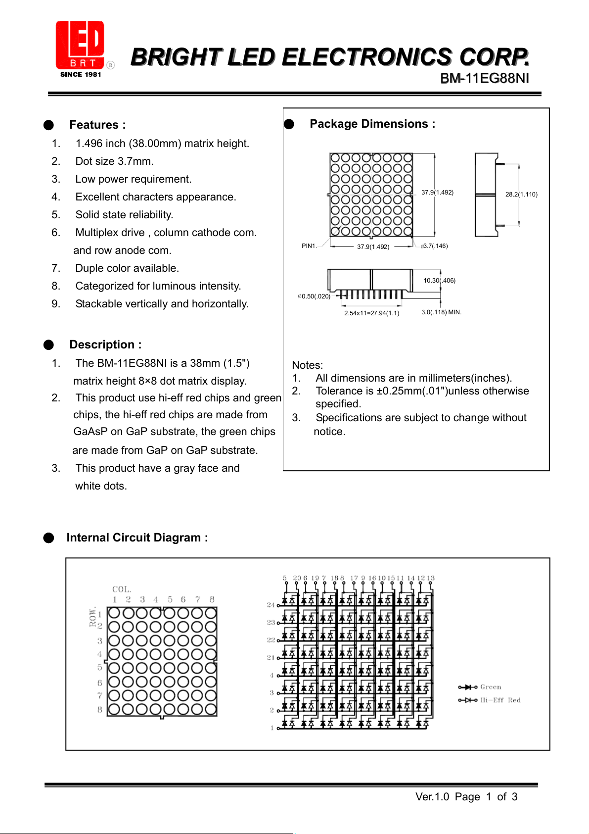
BRIGHT LED ELECTRONICS CORP. SINCE 1981 BM-11EG88NI ● Features : ● Package Dimensions : 1.
1.496 inch (38.00mm) matrix height. 2. Dot size 3.7mm. 3. Low power requirement. 37.9(1.492) 28.2(1.110) 4.
Excellent characters appearance. 5. Solid state reliability. 6.
Multiplex drive , column cathode com. PIN1. 37.9(1.492) 3.7(.146) and row anode com. 7. Duple color available. 10.30(.406) 8.
Categorized for luminous intensity. 0.50(.020) 9.
Stackable vertically and horizontally. 2.54x11=27.94(1.1) 3.0(.118) MIN. ● Description : 1.
The BM-11EG88NI is a 38mm (1.5") Notes: 1.
All dimensions are in millimeters(inches).
matrix height 8×8 dot matrix display. 2.
Tolerance is ±0.25mm(.01")unless otherwise 2.
This product use hi-eff red chips and green specified.
chips, the hi-eff red chips are made from 3.
Specifications are subject to change without
GaAsP on GaP substrate, the green chips notice.
are made from GaP on GaP substrate. 3.
This product have a gray face and white dots.
● Internal Circuit Diagram : Ver.1.0 Page 1 of 3
BRIGHT LED ELECTRONICS CORP. SINCE 1981 BM-11EG88NI
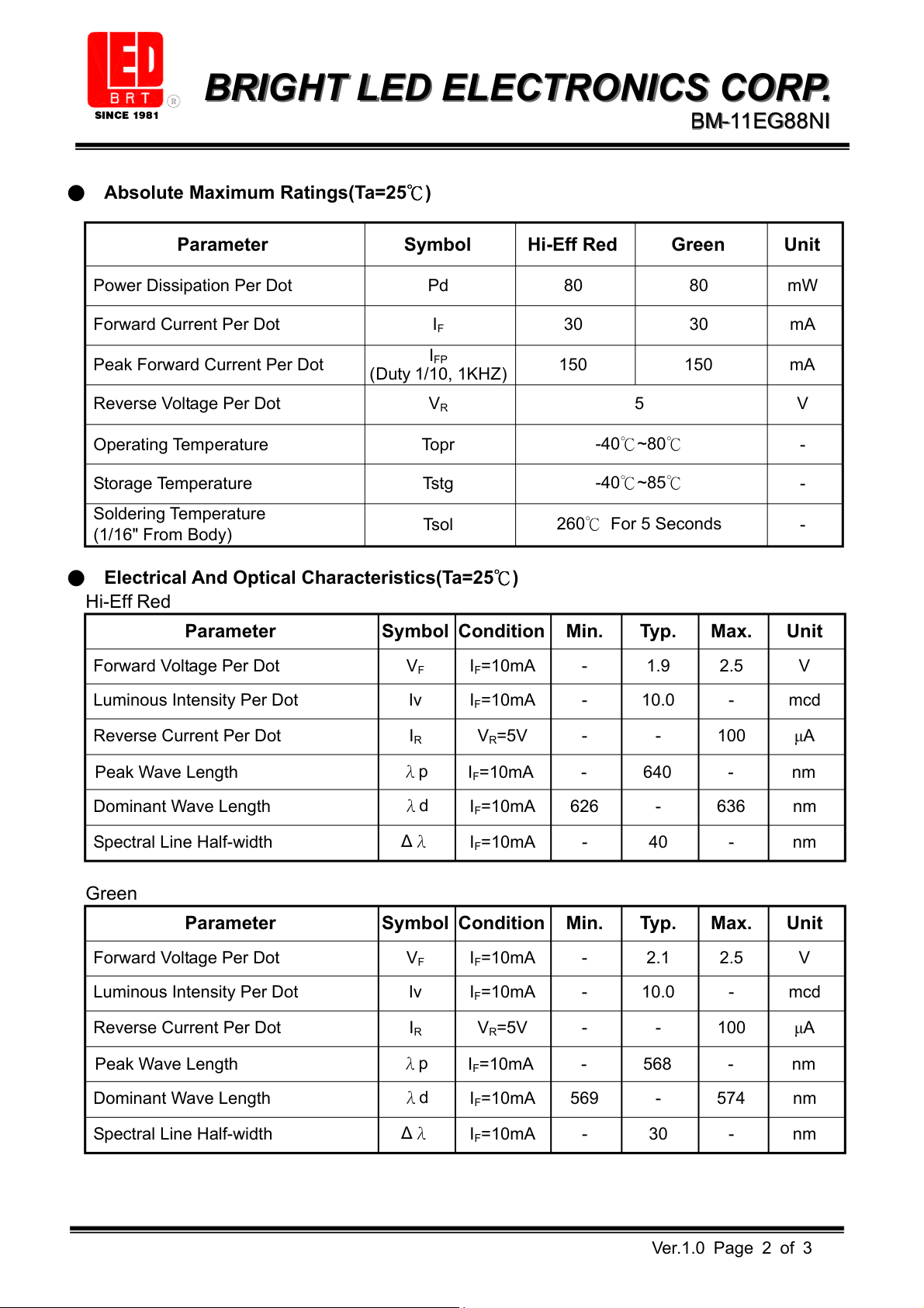
● Absolute Maximum Ratings(Ta=25℃) Parameter Symbol Hi-Eff Red Green Unit Power Dissipation Per Dot Pd 80 80 mW Forward Current Per Dot IF 30 30 mA I Peak Forward Current Per Dot FP 150 150 mA (Duty 1/10, 1KHZ) Reverse Voltage Per Dot VR 5 V Operating Temperature Topr -40℃~80℃ - Storage Temperature Tstg -40℃~85℃ - Soldering Temperature Tsol 260℃ For 5 Seconds - (1/16" From Body)
● Electrical And Optical Characteristics(Ta=25℃) Hi-Eff Red Parameter Symbol Condition Min. Typ. Max. Unit Forward Voltage Per Dot VF IF=10mA - 1.9 2.5 V Luminous Intensity Per Dot Iv IF=10mA - 10.0 - mcd Reverse Current Per Dot IR VR=5V - - 100 µA Peak Wave Length λp IF=10mA - 640 - nm Dominant Wave Length λd IF=10mA 626 - 636 nm Spectral Line Half-width ∆λ IF=10mA - 40 - nm Green Parameter Symbol Condition Min. Typ. Max. Unit Forward Voltage Per Dot VF IF=10mA - 2.1 2.5 V Luminous Intensity Per Dot Iv IF=10mA - 10.0 - mcd Reverse Current Per Dot IR VR=5V - - 100 µA Peak Wave Length λp IF=10mA - 568 - nm Dominant Wave Length λd IF=10mA 569 - 574 nm Spectral Line Half-width ∆λ IF=10mA - 30 - nm Ver.1.0 Page 2 of 3
BRIGHT LED ELECTRONICS CORP. SINCE 1981 BM-11EG88NI
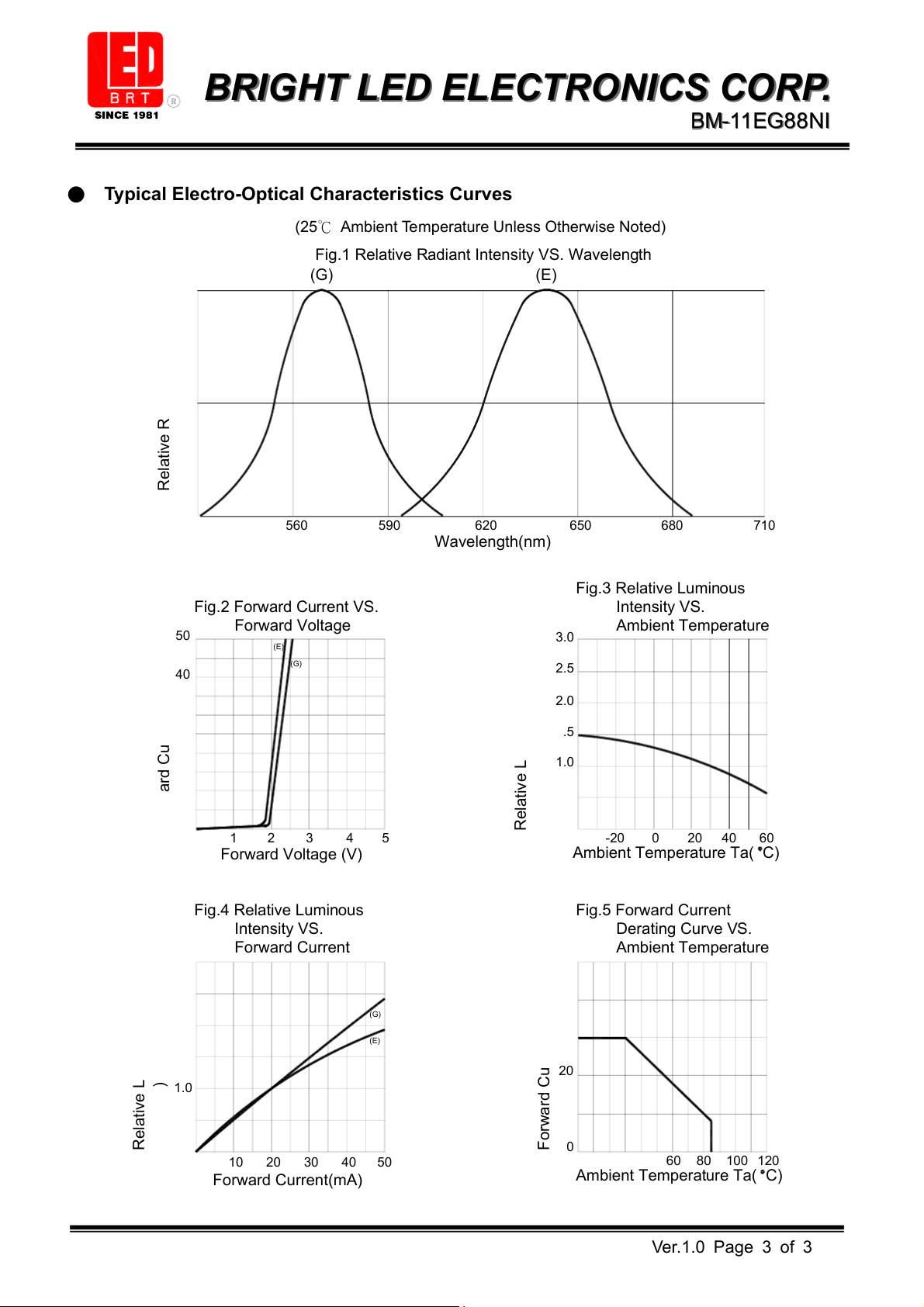
● Typical Electro-Optical Characteristics Curves
(25℃ Ambient Temperature Unless Otherwise Noted)
Fig.1 Relative Radiant Intensity VS. Wavelength (G) (E) 1.0 ity s n te t In n ia d 0.5 a R e tiv la e R 0 530 560 590 620 650 680 710 Wavelength(nm) Fig.3 Relative Luminous Fig.2 Forward Current VS. Intensity VS. Forward Voltage Ambient Temperature 50 3.0 (E) ity s (G) n ) 2.5 40 A te In s 2.0 t (m 30 u n o 1.5 rre in u 20 m u C L ) 1.0 rd e A a 10 m tiv 0 0.5 rw la 2 o e F 0 R (@ 0 1 2 3 4 5 -40 -20 0 20 40 60 Forward Voltage (V) Ambient Temperature Ta( C) Fig.4 Relative Luminous Fig.5 Forward Current Intensity VS. Derating Curve VS. Forward Current Ambient Temperature 3.0 50 sity n te ) 40 In (G) A s u 2.0 o t(m 30 (E) n in m rre u u 20 L ) 1.0 C e A rd tiv m 0 a 10 la 2 e rw o R (@ 0.0 F 0 0 10 20 30 40 50 20 40 60 80 100 120 Forward Current(mA) Ambient Temperature Ta( C) Ver.1.0 Page 3 of 3
Tài liệu liên quan:
-
Báo cáo Thực Tập Cơ Bản: Linh Kiện và IC Trong Mạch Điện | Thực tập cơ bản | Trường Đại học Bách khoa Hà Nội
41 21 -
Báo cáo Thực Tập Cơ Bản: Thiết Kế Mạch Điện Tử | Thực tập cơ bản | Trường Đại học Bách khoa Hà Nội
34 17 -
Báo cáo về Chủ nghĩa Xã hội Khoa học và Vai trò của C. Mác - Ph. Ăngghen | Thực tập cơ bản | Trường Đại học Bách khoa Hà Nội
40 20 -
Báo cáo Thực Tập Cơ Bản: Thiết Kế Mạch Đếm Thuận 0-9 Bằng Altium | Thực tập cơ bản | Trường Đại học Bách khoa Hà Nội
34 17 -
Báo cáo thực tập Mạch khuếch đại âm tần - Điện tử | Thực tập cơ bản | Trường Đại học Bách khoa Hà Nội
35 18