


Preview text:
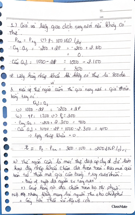
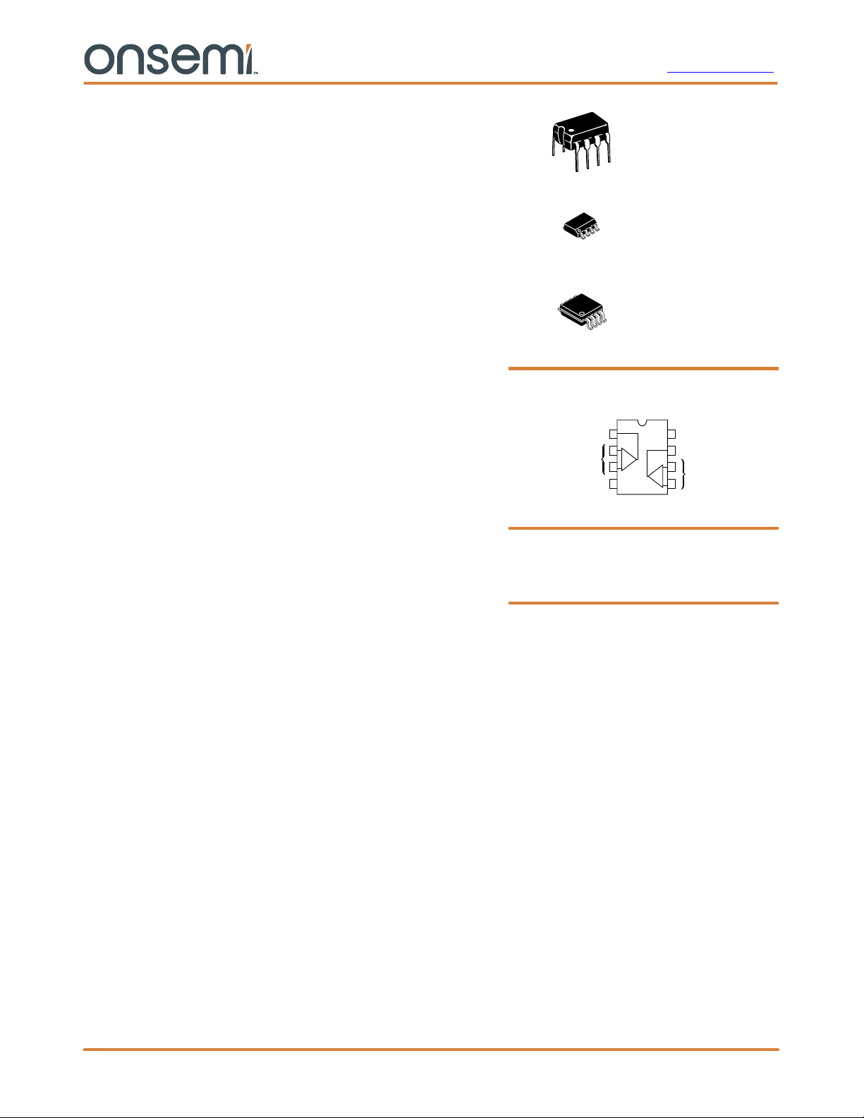
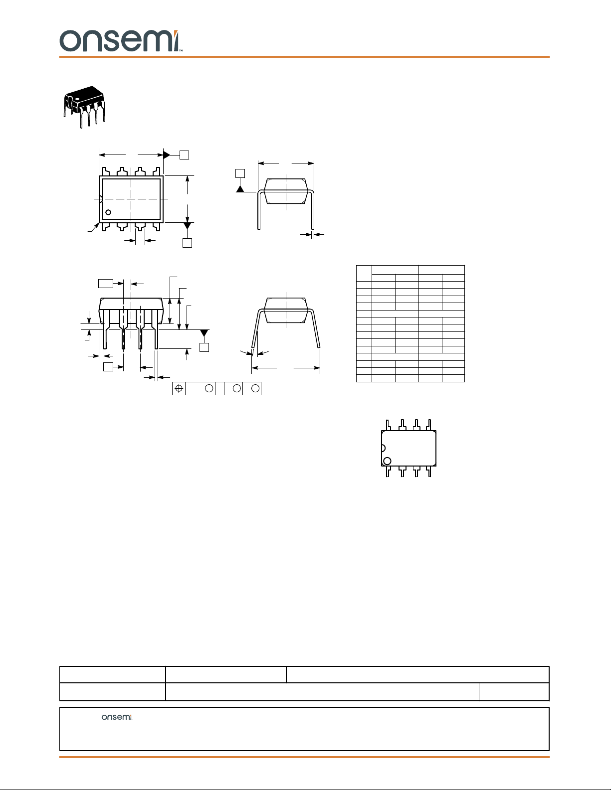
DATA SHEET www.onsemi.com Single Supply Dual Operational Amplifiers PDIP−8 N, AN, VN SUFFIX CASE 626 8 1 LM258, LM358, LM358A, LM358E, LM2904, LM2904A, SOIC−8 D, VD SUFFIX 8 LM2904E, LM2904V, CASE 751 1 NCV2904
Utilizing the circuit designs perfected for Quad Operational Micro8] 8
Amplifiers, these dual operational amplifiers feature low power drain, DMR2 SUFFIX
a common mode input voltage range extending to ground/V CASE 846A EE, and 1
single supply or split supply operation. The LM358 series is
equivalent to one−half of an LM324.
These amplifiers have several distinct advantages over standard PIN CONNECTIONS
operational amplifier types in single supply applications. They can
operate at supply voltages as low as 3.0 V or as high as 32 V, with
quiescent currents about one−fifth of those associated with the Output A 1 8 VCC
MC1741 (on a per amplifier basis). The common mode input range 2 7 Output B − Inputs A +
includes the negative supply, thereby eliminating the necessity for 3 − 6 Inputs B +
external biasing components in many applications. The output voltage VEE/Gnd 4 5
range also includes the negative power supply voltage. (Top View) Features
• Short Circuit Protected Outputs ORDERING INFORMATION
• True Differential Input Stage
See detailed ordering and shipping information on page 10 of this data sheet.
• Single Supply Operation: 3.0 V to 32 V • Low Input Bias Currents •
DEVICE MARKING INFORMATION Internally Compensated
See general marking information in the device marking
• Common Mode Range Extends to Negative Supply
section on page 11 of this data sheet.
• Single and Split Supply Operation
• ESD Clamps on the Inputs Increase Ruggedness of the Device without Affecting Operation
• NCV Prefix for Automotive and Other Applications Requiring
Unique Site and Control Change Requirements; AEC−Q100 Qualified and PPAP Capable
• These Devices are Pb−Free, Halogen Free/BFR Free and are RoHS Compliant
© Semiconductor Components Industries, LLC, 2016 1 Publication Order Number:
September, 2024 − Rev. 36 LM358/D
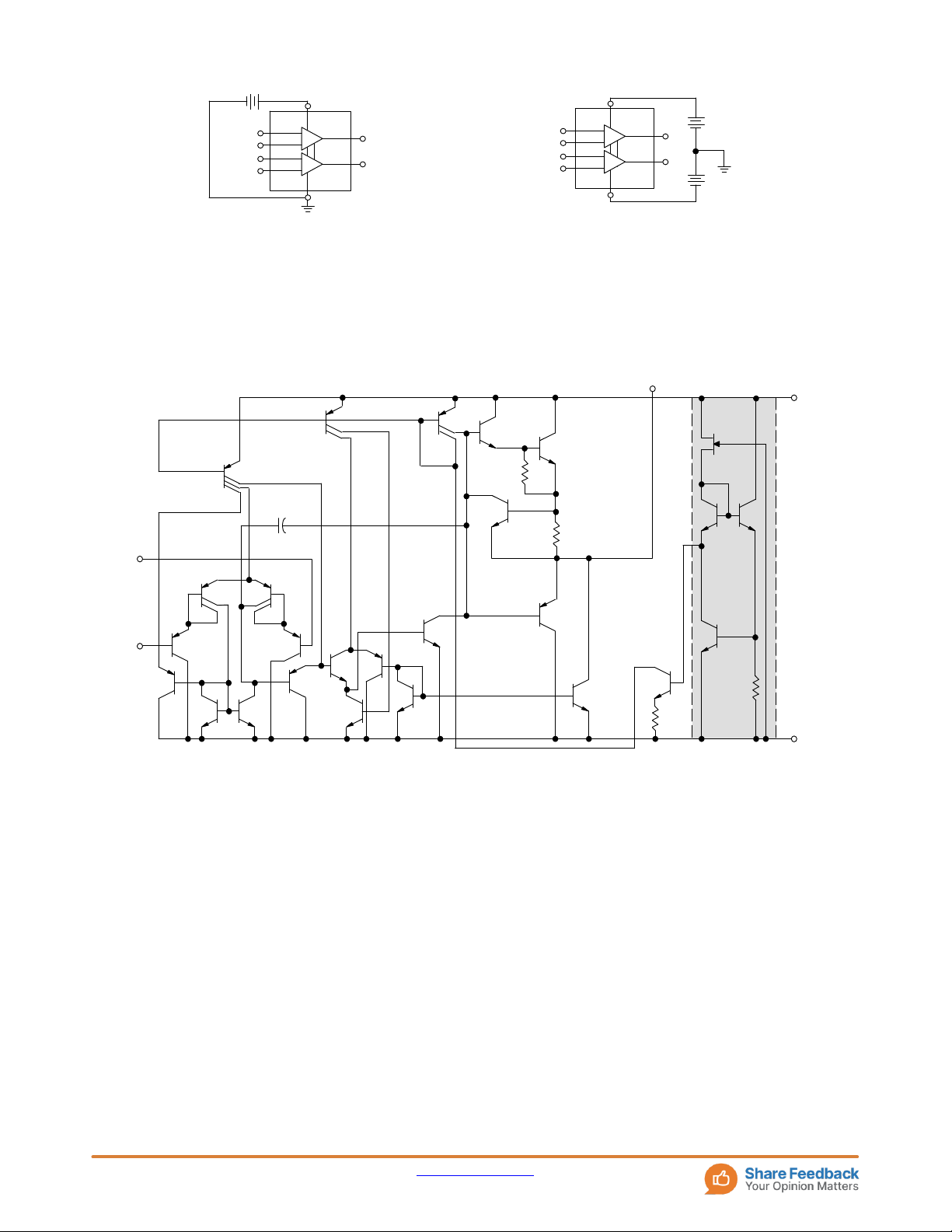
LM258, LM358, LM358A, LM358E, LM2904, LM2904A, LM2904E, LM2904V, NCV2904 3.0 V to VCC(max) VCC VCC 1.5 V to VCC(max) 1 1 2 2 1.5 V to VEE(max) VEE VEE/Gnd Single Supply Split Supplies Figure 1. Bias Circuitry Common to Both Output Amplifiers VCC Q15 Q22 Q16 Q14 Q13 40 k Q19 5.0 pF Q12 Q24 25 Q23 Q18 Q20 Inputs Q11 Q9 Q17 Q21 Q6 Q7 Q25 Q2 Q5 Q1 2.4 k Q8 Q10 Q3 Q4 Q26 2.0 k VEE/Gnd
Figure 2. Representative Schematic Diagram (One−Half of Circuit Shown) www.onsemi.com 2
LM258, LM358, LM358A, LM358E, LM2904, LM2904A, LM2904E, LM2904V, NCV2904
MAXIMUM RATINGS (TA = +25°C, unless otherwise noted.) Rating Symbol Value Unit Power Supply Voltages Vdc Single Supply VCC 32 Split Supplies VCC, VEE ±16
Input Differential Voltage Range (Note 1) VIDR ±32 Vdc
Input Common Mode Voltage Range VICR −0.3 to 32 Vdc Output Short Circuit Duration tSC Continuous Junction Temperature TJ 150 °C
Thermal Resistance, Junction−to−Air (Note 2) Case 846A RJA 238 °C/W Case 751 212 Case 626 161
Thermal Resistance, Junction−to−Case Case 751 RJC 72 °C/W
Thermal Resistance, Junction−to−Board Case 751 RJB 74 °C/W Storage Temperature Range Tstg −65 to +150 °C
Operating Ambient Temperature Range TA °C LM258 −25 to +85 LM358, LM358A, LM358E 0 to +70 LM2904, LM2904A, LM2904E −40 to +105 LM2904V, NCV2904 (Note 3) −40 to +125
Stresses exceeding those listed in the Maximum Ratings table may damage the device. If any of these limits are exceeded, device functionality
should not be assumed, damage may occur and reliability may be affected. 1. Split Power Supplies.
2. All RJA measurements made on evaluation board with 1 oz. copper traces of minimum pad size. All device outputs were active.
3. NCV2904 is qualified for automotive use. ESD RATINGS Rating HBM MM Unit
ESD Protection at any Pin (Human Body Model − HBM, Machine Model − MM) NCV2904 (Note 3) 2000 200 V LM358E, LM2904E 2000 200 V LM358DG/DR2G, LM2904DG/DR2G 250 100 V All Other Devices 2000 200 V www.onsemi.com 3
LM258, LM358, LM358A, LM358E, LM2904, LM2904A, LM2904E, LM2904V, NCV2904
ELECTRICAL CHARACTERISTICS (VCC = 5.0 V, VEE = GND, TA = 25°C, unless otherwise noted.) LM258 LM358, LM358E LM358A Characteristic Symbol Min Typ Max Min Typ Max Min Typ Max Unit Input Offset Voltage VIO mV
VCC = 5.0 V to 30 V, VIC = 0 V to VCC −1.7 V, VO ] 1.4 V, RS = 0 TA = 25°C − 2.0 5.0 − 2.0 7.0 − 2.0 3.0 TA = Thigh (Note 4) − − 7.0 − − 9.0 − − 5.0 TA = Tlow (Note 4) − − 7.0 − − 9.0 − − 5.0
Average Temperature Coefficient of Input Offset VIO/T − 7.0 − − 7.0 − − 7.0 − V/°C Voltage TA = Thigh to Tlow (Note 4) Input Offset Current IIO − 3.0 30 − 5.0 50 − 5.0 30 nA TA = Thigh to Tlow (Note 4) − − 100 − − 150 − − 75 Input Bias Current IIB − −45 −150 − −45 −250 − −45 −100 TA = Thigh to Tlow (Note 4) − −50 −300 − −50 −500 − −50 −200
Average Temperature Coefficient of Input Offset IIO/T − 10 − − 10 − − 10 − pA/°C Current TA = Thigh to Tlow (Note 4)
Input Common Mode Voltage Range (Note 5), VICR 0 − 28.3 0 − 28.3 0 − 28.5 V VCC = 30 V VCC = 30 V, TA = Thigh to Tlow 0 − 28 0 − 28 0 − 28
Differential Input Voltage Range VIDR − − VCC − − VCC − − VCC V
Large Signal Open Loop Voltage Gain AVOL V/mV
RL = 2.0 k, VCC = 15 V, For Large VO Swing, 50 100 − 25 100 − 25 100 − TA = Thigh to Tlow (Note 4) 25 − − 15 − − 15 − − Channel Separation CS − −120 − − −120 − − −120 − dB
1.0 kHz ≤ f ≤ 20 kHz, Input Referenced Common Mode Rejection CMR 70 85 − 65 70 − 65 70 − dB RS ≤ 10 k Power Supply Rejection PSR 65 100 − 65 100 − 65 100 − dB Output Voltage−High Limit VOH V TA = Thigh to Tlow (Note 4)
VCC = 5.0 V, RL = 2.0 k, TA = 25°C 3.3 3.5 − 3.3 3.5 − 3.3 3.5 − VCC = 30 V, RL = 2.0 k 26 − − 26 − − 26 − − VCC = 30 V, RL = 10 k 27 28 − 27 28 − 27 28 − Output Voltage−Low Limit VOL − 5.0 20 − 5.0 20 − 5.0 20 mV VCC = 5.0 V, RL = 10 k, TA = Thigh to Tlow (Note 4) Output Source Current IO+ mA VID = +1.0 V, VCC = 15 V 20 40 − 20 40 − 20 40 −
TA = Thigh to Tlow (LM358A Only) 10 − − Output Sink Current IO− VID = −1.0 V, VCC = 15 V 10 20 − 10 20 − 10 20 − mA
TA = Thigh to Tlow (LM358A Only) 5.0 − − mA VID = −1.0 V, VO = 200 mV 12 50 − 12 50 − 12 50 − A
Output Short Circuit to Ground (Note 6) ISC − 40 60 − 40 60 − 40 60 mA
Power Supply Current (Total Device) ICC mA TA = Thigh to Tlow (Note 4) VCC = 30 V, VO = 0 V, RL = ∞ − 1.5 3.0 − 1.5 3.0 − 1.5 2.0 VCC = 5 V, VO = 0 V, RL = ∞ − 0.7 1.2 − 0.7 1.2 − 0.7 1.2
4. LM258: Tlow = −25°C, Thigh = +85°C
LM358, LM358A, LM358E: Tlow = 0°C, Thigh = +70°C
LM2904/A/E: Tlow = −40°C, Thigh = +105°C
LM2904V & NCV2904: Tlow = −40°C, Thigh = +125°C
NCV2904 is qualified for automotive use.
5. The input common mode voltage or either input signal voltage should not be allowed to go negative by more than 0.3 V. The upper end of
the common mode voltage range is VCC − 1.7 V, but either or both inputs can go to +32 V without damage, independent of the magnitude of VCC.
6. Short circuits from the output to VCC can cause excessive heating and eventual destruction. Destructive dissipation can result from
simultaneous shorts on all amplifiers. www.onsemi.com 4
LM258, LM358, LM358A, LM358E, LM2904, LM2904A, LM2904E, LM2904V, NCV2904
ELECTRICAL CHARACTERISTICS (VCC = 5.0 V, VEE = Gnd, TA = 25°C, unless otherwise noted.) LM2904/LM2904E LM2904A LM2904V, NCV2904 Characteristic Symbol Min Typ Max Min Typ Max Min Typ Max Unit Input Offset Voltage VIO mV
VCC = 5.0 V to 30 V, VIC = 0 V to VCC −1.7 V, VO ] 1.4 V, RS = 0 TA = 25°C − 2.0 7.0 − 2.0 7.0 − − 7.0 TA = Thigh (Note 7) − − 10 − − 10 − − 13 TA = Tlow (Note 7) − − 10 − − 10 − − 10
Average Temperature Coefficient of Input Offset VIO/T − 7.0 − − 7.0 − − 7.0 − V/°C Voltage TA = Thigh to Tlow (Note 7) Input Offset Current IIO − 5.0 50 − 5.0 50 − 5.0 50 nA TA = Thigh to Tlow (Note 7) − 45 200 − 45 200 − 45 200 Input Bias Current IIB − −45 −250 − −45 −100 − −45 −250 TA = Thigh to Tlow (Note 7) − −50 −500 − −50 −250 − −50 −500
Average Temperature Coefficient of Input Offset IIO/T − 10 − − 10 − − 10 − pA/°C Current TA = Thigh to Tlow (Note 7)
Input Common Mode Voltage Range (Note 8), VICR 0 − 28.3 0 − 28.3 0 − 28.3 V VCC = 30 V VCC = 30 V, TA = Thigh to Tlow 0 − 28 0 − 28 0 − 28
Differential Input Voltage Range VIDR − − VCC − − VCC − − VCC V
Large Signal Open Loop Voltage Gain AVOL V/mV
RL = 2.0 k, VCC = 15 V, For Large VO Swing, 25 100 − 25 100 − 25 100 − TA = Thigh to Tlow (Note 7) 15 − − 15 − − 15 − − Channel Separation CS − −120 − − −120 − − −120 − dB
1.0 kHz ≤ f ≤ 20 kHz, Input Referenced Common Mode Rejection CMR 50 70 − 50 70 − 50 70 − dB RS ≤ 10 k Power Supply Rejection PSR 50 100 − 50 100 − 50 100 − dB Output Voltage−High Limit VOH V TA = Thigh to Tlow (Note 7)
VCC = 5.0 V, RL = 2.0 k, TA = 25°C 3.3 3.5 − 3.3 3.5 − 3.3 3.5 − VCC = 30 V, RL = 2.0 k 26 − − 26 − − 26 − − VCC = 30 V, RL = 10 k 27 28 − 27 28 − 27 28 − Output Voltage−Low Limit VOL − 5.0 20 − 5.0 20 − 5.0 20 mV VCC = 5.0 V, RL = 10 k, TA = Thigh to Tlow (Note 7) Output Source Current IO+ 20 40 − 20 40 − 20 40 − mA VID = +1.0 V, VCC = 15 V Output Sink Current IO− VID = −1.0 V, VCC = 15 V 10 20 − 10 20 − 10 20 − mA VID = −1.0 V, VO = 200 mV − − − − − − − − − A
Output Short Circuit to Ground (Note 9) ISC − 40 60 − 40 60 − 40 60 mA
Power Supply Current (Total Device) ICC mA TA = Thigh to Tlow (Note 7) VCC = 30 V, VO = 0 V, RL = ∞ − 1.5 3.0 − 1.5 3.0 − 1.5 3.0 VCC = 5 V, VO = 0 V, RL = ∞ − 0.7 1.2 − 0.7 1.2 − 0.7 1.2
7. LM258: Tlow = −25°C, Thigh = +85°C
LM358, LM358A, LM358E: Tlow = 0°C, Thigh = +70°C
LM2904/A/E: Tlow = −40°C, Thigh = +105°C
LM2904V & NCV2904: Tlow = −40°C, Thigh = +125°C
NCV2904 is qualified for automotive use.
8. The input common mode voltage or either input signal voltage should not be allowed to go negative by more than 0.3 V. The upper end of
the common mode voltage range is VCC − 1.7 V, but either or both inputs can go to +32 V without damage, independent of the magnitude of VCC.
9. Short circuits from the output to VCC can cause excessive heating and eventual destruction. Destructive dissipation can result from
simultaneous shorts on all amplifiers.
Product parametric performance is indicated in the Electrical Characteristics for the listed test conditions, unless otherwise noted. Product
performance may not be indicated by the Electrical Characteristics if operated under different conditions. www.onsemi.com 5
LM258, LM358, LM358A, LM358E, LM2904, LM2904A, LM2904E, LM2904V, NCV2904 CIRCUIT DESCRIPTION
The LM358 series is made using two internally V
compensated, two−stage operational amplifiers. The first CC = 15 Vdc RL = 2.0 k
stage of each consists of differential input devices Q20 and TA = 25°C
Q18 with input buffer transistors Q21 and Q17 and the
differential to single ended converter Q3 and Q4. The first
stage performs not only the first stage gain function but also
performs the level shifting and transconductance reduction 1.0 V/DIV
functions. By reducing the transconductance, a smaller
compensation capacitor (only 5.0 pF) can be employed, thus
saving chip area. The transconductance reduction is
accomplished by splitting the collectors of Q20 and Q18.
Another feature of this input stage is that the input common 5.0 s/DIV
mode range can include the negative supply or ground, in
single supply operation, without saturating either the input
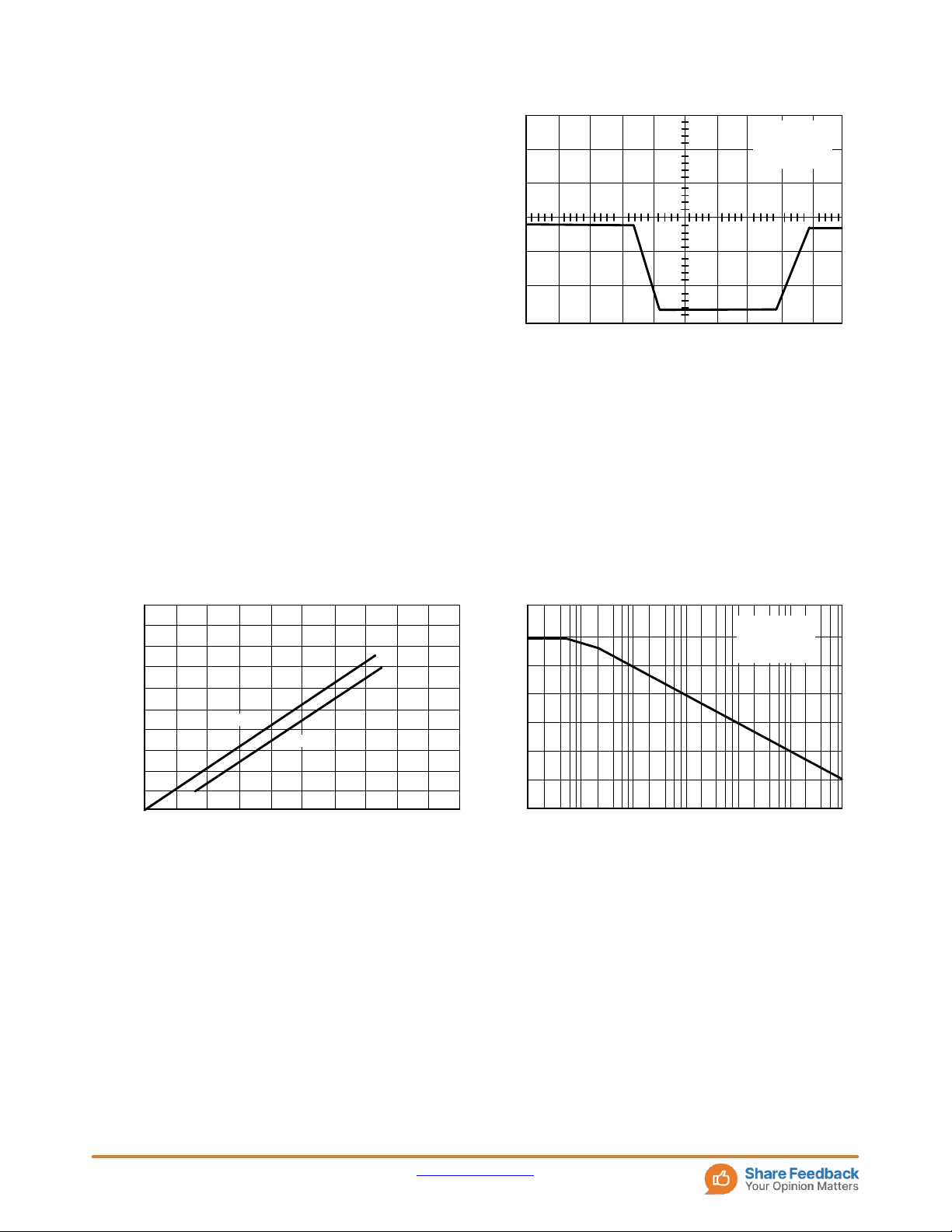
Figure 3. Large Signal Voltage
devices or the differential to single−ended converter. The Follower Response
second stage consists of a standard current source load amplifier stage.
Each amplifier is biased from an internal−voltage
regulator which has a low temperature coefficient thus
giving each amplifier good temperature characteristics as
well as excellent power supply rejection. 20 120 18 VCC = 15 V 100 V 16 EE = Gnd TA = 25°C 14 80 TAGE (V) TAGE GAIN (dB) 12 60 VOL VOL 10 Negative 8.0 40 Positive IV , INPUT 6.0 20 4.0 , OPEN LOOP 0 2.0 VOLA 0 -20 0 2.0 4.0 6.0 8.0 10 12 14 16 18 20 1.0 10 100 1.0 k 10 k 100 k 1.0 M
VCC/VEE, POWER SUPPLY VOLTAGES (V) f, FREQUENCY (Hz)
Figure 4. Input Voltage Range
Figure 5. Large−Signal Open Loop Voltage Gain www.onsemi.com 6
LM258, LM358, LM358A, LM358E, LM2904, LM2904A, LM2904E, LM2904V, NCV2904 14 ) 550 V pp CC = 30 V R 12 L = 2.0 k 500 VEE = Gnd VCC = 15 V Input TA = 25°C VEE = Gnd 10 450 CL = 50 pF Gain = -100 R TAGE (mV) I = 1.0 k 400 8.0 R Output F = 100 k TAGE RANGE (V VOL 350 VOL 6.0 300 , OUTPUT 4.0 OV 250 , OUTPUT 2.0 OR 200 V 0 0 1.0 10 100 1000 0 1.0 2.0 3.0 4.0 5.0 6.0 7.0 8.0 f, FREQUENCY (kHz) t, TIME s)
Figure 6. Large−Signal Frequency Response
Figure 7. Small Signal Voltage Follower
Pulse Response (Noninverting) 2.4 2.1 T (mA) A = 25°C RL = R 90 1.8 (nA) 1.5 CURRENT Y 1.2 0.9 80 BIAS CURRENT 0.6 0.3 IB I , POWER SUPPL CC I , INPUT 0 70 0 5.0 10 15 20 25 30 35 0 2.0 4.0 6.0 8.0 10 12 14 16 18 20 VCC, POWER SUPPLY VOLTAGE (V) VCC, POWER SUPPLY VOLTAGE (V)
Figure 8. Power Supply Current versus
Figure 9. Input Bias Current versus Power Supply Voltage Supply Voltage www.onsemi.com 7
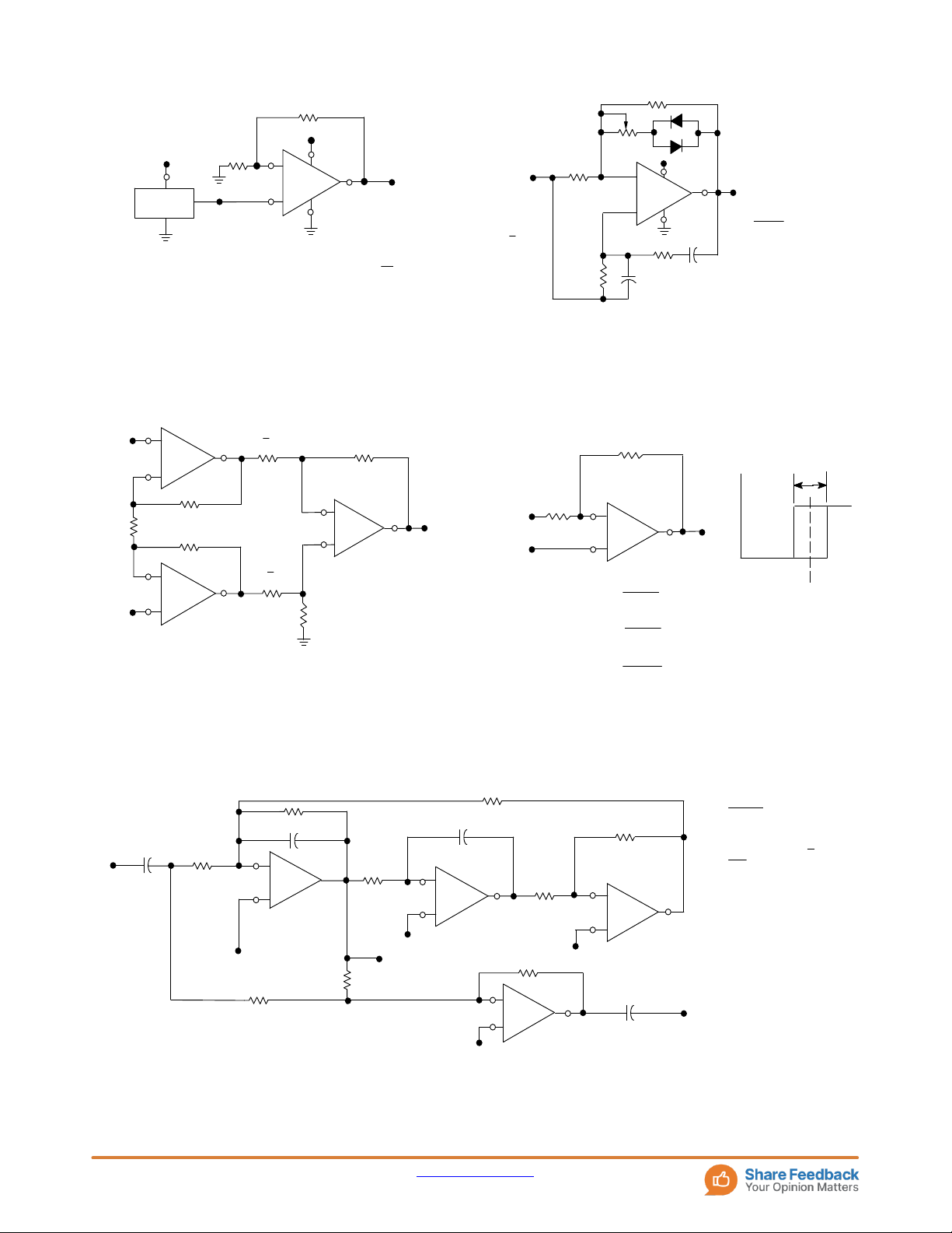
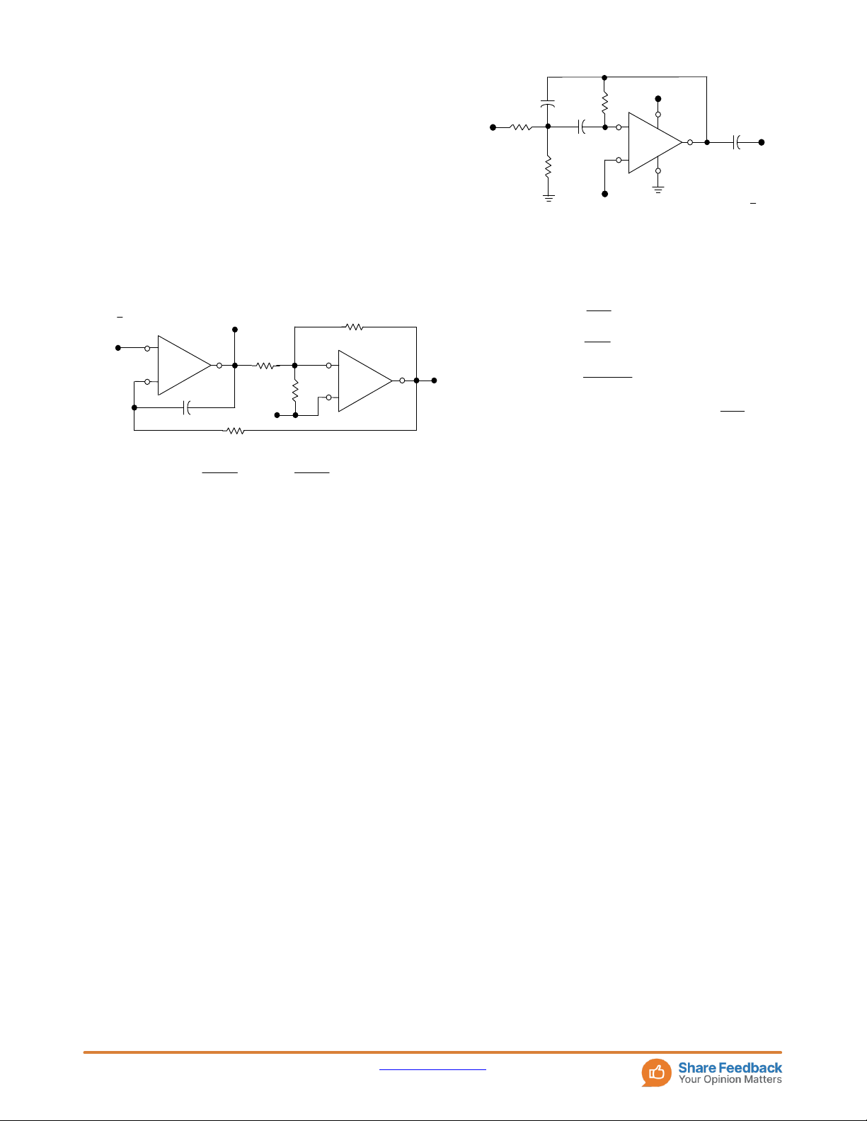
LM258, LM358, LM358A, LM358E, LM2904, LM2904A, LM2904E, LM2904V, NCV2904 50 k R1 V V CC 5.0 k CC R2 - 10 k V 1/2 - CC V V LM358 O ref 1/2 V MC1403 + LM358 O 2.5 V + 1 f 1 o = 2 RC Vref = VCC 2 For: fo = 1.0 kHz R1 V ) R R = 16 k O = 2.5 V (1 + R2 R C C C = 0.01 F
Figure 10. Voltage Reference
Figure 11. Wien Bridge Oscillator 1 e + R 1 C R 1/2 LM358 R2 Hysteresis - VOH R1 - V a R1 V + O 1/2 ref R1 e 1/2 LM358 o LM358 + Vin - VO b R1 VOL 1 V - R inL VinH C 1/2 R1 V V inL = (V ref LM358 R1 + R2 OL - Vref)+ Vref e + 2 R R1 VinH = (V R1 + R2 OH - Vref) + Vref eo = C (1 + a + b) (e2 - e1) R1 H = (V R1 + R2 OH - VOL)
Figure 12. High Impedance Differential Amplifier
Figure 13. Comparator with Hysteresis 1 R fo = 2 R 100 k RC R1 = QR 1 C1 V V = V in R2 C C R1 ref 2 CC - R2 = R TBP 1/2 - LM358 100 k 1/2 - R3 = TN R2 + LM358 1/2 C1 = 10 C + LM358 + Vref For: fo = 1.0 kHz Vref Bandpass Q = 10 V R3 ref Output TBP = 1 T = 1 R1 N R2 - C1 1/2 Notch Output LM358 R = 160 k + C = 0.001 F R1 = 1.6 M Vref Where: T R2 = 1.6 M BP = Center Frequency Gain T R3 = 1.6 M N = Passband Notch Gain
Figure 14. Bi−Quad Filter www.onsemi.com 8
LM258, LM358, LM358A, LM358E, LM2904, LM2904A, LM2904E, LM2904V, NCV2904 VCC C R3 R1 C V - in 1/2 VO LM358 + CO R2 CO = 10 C Vref 1 V ref = VCC 2 Given: fo = center frequency
A(fo) = gain at center frequency Choose value fo, C Q 1 Then: R3 = V Triangle Wave ref = VCC R2 f 2 o C Output R3 300 k R1 = Vref + 2 A(fo) R3 1/2 + LM358 R1 R3 75 k 1/2 R2 = - LM358 4Q2 R1 -R3 R1 100 k Square - Wave Q
For less than 10% error from operational amplifier. o fo < 0.1 Vref Output BW C
Where fo and BW are expressed in Hz. Rf R1 + RC R2 R1
If source impedance varies, filter may be preceded with voltage f = if, R3 = 4 CR R2 + R1
follower buffer to stabilize filter parameters. f R1
Figure 15. Function Generator
Figure 16. Multiple Feedback Bandpass Filter www.onsemi.com 9
LM258, LM358, LM358A, LM358E, LM2904, LM2904A, LM2904E, LM2904V, NCV2904 ORDERING INFORMATION Device
Operating Temperature Range Package Shipping† LM358ADR2G 2500 / Tape & Reel SOIC−8 LM358DG 98 Units / Rail (Pb−Free) LM358DR2G 2500 / Tape & Reel LM358EDR2G SOIC−8 2500 / Tape & Reel 0°C to +70°C (Pb−Free) LM358DMR2G Micro8 4000 / Tape & Reel (Pb−Free) LM358NG PDIP−8 50 Units / Rail (Pb−Free) LM258DG SOIC−8 98 Units / Rail (Pb−Free) LM258DR2G 2500 / Tape & Reel LM258DMR2G −25°C to +85°C Micro8 4000 / Tape & Reel (Pb−Free) LM258NG PDIP−8 50 Units / Rail (Pb−Free) LM2904DG SOIC−8 98 Units / Rail (Pb−Free) LM2904DR2G 2500 / Tape & Reel LM2904EDR2G SOIC−8 2500 / Tape & Reel (Pb−Free) LM2904DMR2G Micro8 2500 / Tape & Reel (Pb−Free) −40°C to +105°C LM2904NG PDIP−8 50 Units / Rail (Pb−Free) LM2904ADMG Micro8 4000 / Tape & Reel (Pb−Free) LM2904ADMR2G 4000 / Tape & Reel LM2904ANG PDIP−8 50 Units / Rail (Pb−Free) LM2904VDG SOIC−8 98 Units / Rail (Pb−Free) LM2904VDR2G 2500 / Tape & Reel LM2904VDMR2G Micro8 4000 / Tape & Reel (Pb−Free) LM2904VNG −40°C to +125°C PDIP−8 50 Units / Rail (Pb−Free) NCV2904DR2G* SOIC−8 2500 / Tape & Reel (Pb−Free) NCV2904DMR2G* Micro8 4000 / Tape & Reel (Pb−Free)
†For information on tape and reel specifications, including part orientation and tape sizes, please refer to our Tape and Reel Packaging
Specifications Brochure, BRD8011/D.
*NCV Prefix for Automotive and Other Applications Requiring Unique Site and Control Change Requirements; AEC−Q100 Qualified and PPAP Capable. www.onsemi.com 10
LM258, LM358, LM358A, LM358E, LM2904, LM2904A, LM2904E, LM2904V, NCV2904 MARKING DIAGRAMS PDIP−8 PDIP−8 PDIP−8 N SUFFIX AN SUFFIX VN SUFFIX CASE 626 CASE 626 CASE 626 8 8 8 8 LMx58N LM2904N LM2904AN LM2904VN AWL AWL AWL AWL YYWWG YYWWG YYWWG YYWWG 1 1 1 1 SOIC−8 SOIC−8 D SUFFIX VD SUFFIX CASE 751 CASE 751 8 8 8 8 * LMx58 LM358 2904 2904V ALYW ALYWA ALYW ALYW G G G G 1 1 1 1 8 8 358E 2904E ALYWA ALYW G G 1 1 Micro8 DMR2 SUFFIX CASE 846A 8 8 8 8 x58 2904 904A 904V * AYWG AYWG AYWG AYWG G G G G 1 1 1 1 x = 2 or 3
*This diagram also applies to NCV2904 A = Assembly Location WL, L = Wafer Lot YY, Y = Year WW, W = Work Week G = Pb−Free Package G
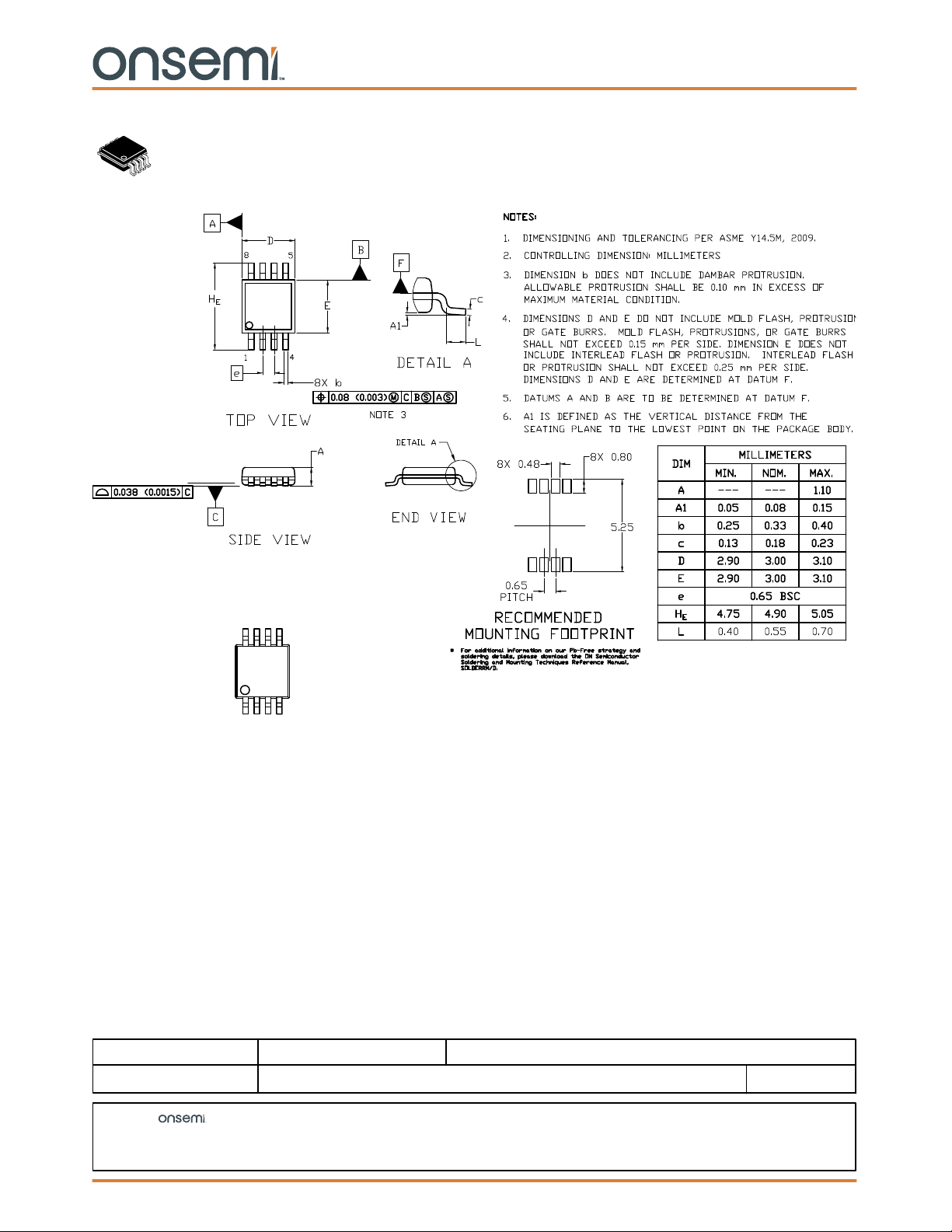
= Pb−Free Package − (Note: Microdot may be in either location) www.onsemi.com 11 MECHANICAL CASE OUTLINE PACKAGE DIMENSIONS PDIP−8 CASE 626−05 ISSUE P DATE 22 APR 2015 SCALE 1:1 D A NOTES:
1. DIMENSIONING AND TOLERANCING PER ASME Y14.5M, 1994. E
2. CONTROLLING DIMENSION: INCHES.
3. DIMENSIONS A, A1 AND L ARE MEASURED WITH THE PACK- H
AGE SEATED IN JEDEC SEATING PLANE GAUGE GS−3. 8 5
4. DIMENSIONS D, D1 AND E1 DO NOT INCLUDE MOLD FLASH
OR PROTRUSIONS. MOLD FLASH OR PROTRUSIONS ARE NOT TO EXCEED 0.10 INCH. E1
5. DIMENSION E IS MEASURED AT A POINT 0.015 BELOW DATUM
PLANE H WITH THE LEADS CONSTRAINED PERPENDICULAR 1 4 TO DATUM C.
6. DIMENSION eB IS MEASURED AT THE LEAD TIPS WITH THE NOTE 8 LEADS UNCONSTRAINED. c b2
7. DATUM PLANE H IS COINCIDENT WITH THE BOTTOM OF THE B END VIEW
LEADS, WHERE THE LEADS EXIT THE BODY. TOP VIEW WITH LEADS CONSTRAINED
8. PACKAGE CONTOUR IS OPTIONAL (ROUNDED OR SQUARE CORNERS). NOTE 5 INCHES MILLIMETERS A2 DIM MIN MAX MIN MAX e/2 A A −−−− 0.210 −−− 5.33 NOTE 3 A1 0.015 −−−− 0.38 −−− A2 0.115 0.195 2.92 4.95 L b 0.014 0.022 0.35 0.56 b2 0.060 TYP 1.52 TYP C 0.008 0.014 0.20 0.36 SEATING D 0.355 0.400 9.02 10.16 A1 PLANE D1 0.005 −−−− 0.13 −−− C E 0.300 0.325 7.62 8.26 M E1 0.240 0.280 6.10 7.11 D1 e 0.100 BSC 2.54 BSC e eB eB −−−− 0.430 −−− 10.92 L 0.115 0.150 2.92 3.81 8X b END VIEW M −−−− 10 ° −−− 10 ° 0.010 M C A SIDE VIEW M B M NOTE 6 GENERIC MARKING DIAGRAM* STYLE 1: PIN 1. AC IN 2. DC + IN XXXXXXXXX 3. DC − IN AWL 4. AC IN 5. GROUND YYWWG 6. OUTPUT 7. AUXILIARY 8. VCC XXXX = Specific Device Code A = Assembly Location WL = Wafer Lot YY = Year WW = Work Week G = Pb−Free Package
*This information is generic. Please refer to
device data sheet for actual part marking.
Pb−Free indicator, “G” or microdot “G”, may
or may not be present. Some products may
not follow the Generic Marking.
DOCUMENT NUMBER: 98ASB42420B
Electronic versions are uncontrolled except when accessed directly from the Document Repository.
Printed versions are uncontrolled except when stamped “CONTROLLED COPY” in red. DESCRIPTION: PDIP−8 PAGE 1 OF 1
onsemi and are trademarks of Semiconductor Components Industries, LLC dba onsemi or its subsidiaries in the United States and/or other countries. onsemi reserves
the right to make changes without further notice to any products herein. onsemi makes no warranty, representation or guarantee regarding the suitability of its products for any particular
purpose, nor does onsemi assume any liability arising out of the application or use of any product or circuit, and specifically disclaims any and all liability, including without limitation
special, consequential or incidental damages. onsemi does not convey any license under its patent rights nor the rights of others.
© Semiconductor Components Industries, LLC, 2019 www.onsemi.com MECHANICAL CASE OUTLINE PACKAGE DIMENSIONS SOIC−8 NB 8 CASE 751−07 1 ISSUE AK DATE 16 FEB 2011 SCALE 1:1 NOTES:
1. DIMENSIONING AND TOLERANCING PER −X− ANSI Y14.5M, 1982. A
2. CONTROLLING DIMENSION: MILLIMETER.
3. DIMENSION A AND B DO NOT INCLUDE MOLD PROTRUSION.
4. MAXIMUM MOLD PROTRUSION 0.15 (0.006) 8 5 PER SIDE.
5. DIMENSION D DOES NOT INCLUDE DAMBAR B S 0.25 (0.010) M Y M PROTRUSION. ALLOWABLE DAMBAR
PROTRUSION SHALL BE 0.127 (0.005) TOTAL 1
IN EXCESS OF THE D DIMENSION AT 4 −Y− K MAXIMUM MATERIAL CONDITION.
6. 751−01 THRU 751−06 ARE OBSOLETE. NEW STANDARD IS 751−07. MILLIMETERS INCHES G DIM MIN MAX MIN MAX A 4.80 5.00 0.189 0.197 C N X 45_ B 3.80 4.00 0.150 0.157 SEATING C 1.35 1.75 0.053 0.069 PLANE D 0.33 0.51 0.013 0.020 −Z− G 1.27 BSC 0.050 BSC H 0.10 0.25 0.004 0.010 0.10 (0.004) J 0.19 0.25 0.007 0.010 H M J D K 0.40 1.27 0.016 0.050 M 0 8 0 8 _ _ _ _ N 0.25 0.50 0.010 0.020 S 5.80 6.20 0.228 0.244 0.25 (0.010) M Z Y S X S GENERIC MARKING DIAGRAM* SOLDERING FOOTPRINT* 8 8 8 8 XXXXX XXXXX XXXXXX XXXXXX ALYWX ALYWX AYWW 1.52 AYWW G G 0.060 1 1 1 1 IC IC Discrete Discrete (Pb−Free) (Pb−Free) 7.0 4.0 XXXXX = Specific Device Code XXXXXX = Specific Device Code 0.275 0.155 A = Assembly Location A = Assembly Location L = Wafer Lot Y = Year Y = Year WW = Work Week W = Work Week G = Pb−Free Package G = Pb−Free Package 0.6 1.270
*This information is generic. Please refer to 0.024 0.050
device data sheet for actual part marking.
Pb−Free indicator, “G” or microdot “G”, may
or may not be present. Some products may SCALE 6:1 ǒ mm Ǔ inches
not follow the Generic Marking.
*For additional information on our Pb−Free strategy and soldering
details, please download the onsemi Soldering and Mounting
Techniques Reference Manual, SOLDERRM/D. STYLES ON PAGE 2
DOCUMENT NUMBER: 98ASB42564B
Electronic versions are uncontrolled except when accessed directly from the Document Repository.
Printed versions are uncontrolled except when stamped “CONTROLLED COPY” in red. DESCRIPTION: SOIC−8 NB PAGE 1 OF 2
onsemi and are trademarks of Semiconductor Components Industries, LLC dba onsemi or its subsidiaries in the United States and/or other countries. onsemi reserves
the right to make changes without further notice to any products herein. onsemi makes no warranty, representation or guarantee regarding the suitability of its products for any particular
purpose, nor does onsemi assume any liability arising out of the application or use of any product or circuit, and specifically disclaims any and all liability, including without limitation
special, consequential or incidental damages. onsemi does not convey any license under its patent rights nor the rights of others.
© Semiconductor Components Industries, LLC, 2019 www.onsemi.com SOIC−8 NB CASE 751−07 ISSUE AK DATE 16 FEB 2011 STYLE 1: STYLE 2: STYLE 3: STYLE 4: PIN 1. EMITTER PIN 1. COLLECTOR, DIE, #1 PIN 1. DRAIN, DIE #1 PIN 1. ANODE 2. COLLECTOR 2. COLLECTOR, #1 2. DRAIN, #1 2. ANODE 3. COLLECTOR 3. COLLECTOR, #2 3. DRAIN, #2 3. ANODE 4. EMITTER 4. COLLECTOR, #2 4. DRAIN, #2 4. ANODE 5. EMITTER 5. BASE, #2 5. GATE, #2 5. ANODE 6. BASE 6. EMITTER, #2 6. SOURCE, #2 6. ANODE 7. BASE 7. BASE, #1 7. GATE, #1 7. ANODE 8. EMITTER 8. EMITTER, #1 8. SOURCE, #1 8. COMMON CATHODE STYLE 5: STYLE 6: STYLE 7: STYLE 8: PIN 1. DRAIN PIN 1. SOURCE PIN 1. INPUT PIN 1. COLLECTOR, DIE #1 2. DRAIN 2. DRAIN 2. EXTERNAL BYPASS 2. BASE, #1 3. DRAIN 3. DRAIN 3. THIRD STAGE SOURCE 3. BASE, #2 4. DRAIN 4. SOURCE 4. GROUND 4. COLLECTOR, #2 5. GATE 5. SOURCE 5. DRAIN 5. COLLECTOR, #2 6. GATE 6. GATE 6. GATE 3 6. EMITTER, #2 7. SOURCE 7. GATE 7. SECOND STAGE Vd 7. EMITTER, #1 8. SOURCE 8. SOURCE 8. FIRST STAGE Vd 8. COLLECTOR, #1 STYLE 9: STYLE 10: STYLE 11: STYLE 12: PIN 1. EMITTER, COMMON PIN 1. GROUND PIN 1. SOURCE 1 PIN 1. SOURCE 2. COLLECTOR, DIE #1 2. BIAS 1 2. GATE 1 2. SOURCE 3. COLLECTOR, DIE #2 3. OUTPUT 3. SOURCE 2 3. SOURCE 4. EMITTER, COMMON 4. GROUND 4. GATE 2 4. GATE 5. EMITTER, COMMON 5. GROUND 5. DRAIN 2 5. DRAIN 6. BASE, DIE #2 6. BIAS 2 6. DRAIN 2 6. DRAIN 7. BASE, DIE #1 7. INPUT 7. DRAIN 1 7. DRAIN 8. EMITTER, COMMON 8. GROUND 8. DRAIN 1 8. DRAIN STYLE 13: STYLE 14: STYLE 15: STYLE 16: PIN 1. N.C. PIN 1. N−SOURCE PIN 1. ANODE 1 PIN 1. EMITTER, DIE #1 2. SOURCE 2. N−GATE 2. ANODE 1 2. BASE, DIE #1 3. SOURCE 3. P−SOURCE 3. ANODE 1 3. EMITTER, DIE #2 4. GATE 4. P−GATE 4. ANODE 1 4. BASE, DIE #2 5. DRAIN 5. P−DRAIN 5. CATHODE, COMMON 5. COLLECTOR, DIE #2 6. DRAIN 6. P−DRAIN 6. CATHODE, COMMON 6. COLLECTOR, DIE #2 7. DRAIN 7. N−DRAIN 7. CATHODE, COMMON 7. COLLECTOR, DIE #1 8. DRAIN 8. N−DRAIN 8. CATHODE, COMMON 8. COLLECTOR, DIE #1 STYLE 17: STYLE 18: STYLE 19: STYLE 20: PIN 1. VCC PIN 1. ANODE PIN 1. SOURCE 1 PIN 1. SOURCE (N) 2. V2OUT 2. ANODE 2. GATE 1 2. GATE (N) 3. V1OUT 3. SOURCE 3. SOURCE 2 3. SOURCE (P) 4. TXE 4. GATE 4. GATE 2 4. GATE (P) 5. RXE 5. DRAIN 5. DRAIN 2 5. DRAIN 6. VEE 6. DRAIN 6. MIRROR 2 6. DRAIN 7. GND 7. CATHODE 7. DRAIN 1 7. DRAIN 8. ACC 8. CATHODE 8. MIRROR 1 8. DRAIN STYLE 21: STYLE 22: STYLE 23: STYLE 24: PIN 1. CATHODE 1 PIN 1. I/O LINE 1 PIN 1. LINE 1 IN PIN 1. BASE 2. CATHODE 2 2. COMMON CATHODE/VCC 2. COMMON ANODE/GND 2. EMITTER 3. CATHODE 3 3. COMMON CATHODE/VCC 3. COMMON ANODE/GND 3. COLLECTOR/ANODE 4. CATHODE 4 4. I/O LINE 3 4. LINE 2 IN 4. COLLECTOR/ANODE 5. CATHODE 5 5. COMMON ANODE/GND 5. LINE 2 OUT 5. CATHODE 6. COMMON ANODE 6. I/O LINE 4 6. COMMON ANODE/GND 6. CATHODE 7. COMMON ANODE 7. I/O LINE 5 7. COMMON ANODE/GND 7. COLLECTOR/ANODE 8. CATHODE 6 8. COMMON ANODE/GND 8. LINE 1 OUT 8. COLLECTOR/ANODE STYLE 25: STYLE 26: STYLE 27: STYLE 28: PIN 1. VIN PIN 1. GND PIN 1. ILIMIT PIN 1. SW_TO_GND 2. N/C 2. dv/dt 2. OVLO 2. DASIC_OFF 3. REXT 3. ENABLE 3. UVLO 3. DASIC_SW_DET 4. GND 4. ILIMIT 4. INPUT+ 4. GND 5. IOUT 5. SOURCE 5. SOURCE 5. V_MON 6. IOUT 6. SOURCE 6. SOURCE 6. VBULK 7. IOUT 7. SOURCE 7. SOURCE 7. VBULK 8. IOUT 8. VCC 8. DRAIN 8. VIN STYLE 29: STYLE 30: PIN 1. BASE, DIE #1 PIN 1. DRAIN 1 2. EMITTER, #1 2. DRAIN 1 3. BASE, #2 3. GATE 2 4. EMITTER, #2 4. SOURCE 2 5. COLLECTOR, #2 5. SOURCE 1/DRAIN 2 6. COLLECTOR, #2 6. SOURCE 1/DRAIN 2 7. COLLECTOR, #1 7. SOURCE 1/DRAIN 2 8. COLLECTOR, #1 8. GATE 1
DOCUMENT NUMBER: 98ASB42564B
Electronic versions are uncontrolled except when accessed directly from the Document Repository.
Printed versions are uncontrolled except when stamped “CONTROLLED COPY” in red. DESCRIPTION: SOIC−8 NB PAGE 2 OF 2
onsemi and are trademarks of Semiconductor Components Industries, LLC dba onsemi or its subsidiaries in the United States and/or other countries. onsemi reserves
the right to make changes without further notice to any products herein. onsemi makes no warranty, representation or guarantee regarding the suitability of its products for any particular
purpose, nor does onsemi assume any liability arising out of the application or use of any product or circuit, and specifically disclaims any and all liability, including without limitation
special, consequential or incidental damages. onsemi does not convey any license under its patent rights nor the rights of others. www.onsemi.com 2
© Semiconductor Components Industries, LLC, 2019 www.onsemi.com MECHANICAL CASE OUTLINE PACKAGE DIMENSIONS Micro8 CASE 846A−02 ISSUE K DATE 16 JUL 2020 SCALE 2:1 GENERIC MARKING DIAGRAM* 8 XXXX AYWG G 1 XXXX = Specific Device Code A = Assembly Location Y = Year W = Work Week G = Pb−Free Package STYLE 1: STYLE 2: STYLE 3: PIN 1. SOURCE PIN 1. SOURCE 1 PIN 1. N-SOURCE
(Note: Microdot may be in either location) 2. SOURCE 2. GATE 1 2. N-GATE 3. SOURCE 3. SOURCE 2 3. P-SOURCE
*This information is generic. Please refer to 4. GATE 4. GATE 2 4. P-GATE
device data sheet for actual part marking. 5. DRAIN 5. DRAIN 2 5. P-DRAIN
Pb−Free indicator, “G” or microdot “G”, may 6. DRAIN 6. DRAIN 2 6. P-DRAIN 7. DRAIN 7. DRAIN 1 7. N-DRAIN
or may not be present. Some products may 8. DRAIN 8. DRAIN 1 8. N-DRAIN
not follow the Generic Marking.
DOCUMENT NUMBER: 98ASB14087C
Electronic versions are uncontrolled except when accessed directly from the Document Repository.
Printed versions are uncontrolled except when stamped “CONTROLLED COPY” in red. DESCRIPTION: MICRO8 PAGE 1 OF 1
onsemi and are trademarks of Semiconductor Components Industries, LLC dba onsemi or its subsidiaries in the United States and/or other countries. onsemi reserves
the right to make changes without further notice to any products herein. onsemi makes no warranty, representation or guarantee regarding the suitability of its products for any particular
purpose, nor does onsemi assume any liability arising out of the application or use of any product or circuit, and specifically disclaims any and all liability, including without limitation
special, consequential or incidental damages. onsemi does not convey any license under its patent rights nor the rights of others.
© Semiconductor Components Industries, LLC, 2019 www.onsemi.com onsemi,
, and other names, marks, and brands are registered and/or common law trademarks of Semiconductor Components Industries, LLC dba “onsemi” or its affiliates
and/or subsidiaries in the United States and/or other countries. onsemi owns the rights to a number of patents, trademarks, copyrights, trade secrets, and other intellectual property.
A listing of onsemi’s product/patent coverage may be accessed at www.onsemi.com/site/pdf/Patent−Marking.pdf. onsemi reserves the right to make changes at any time to any
products or information herein, without notice. The information herein is provided “as−is” and onsemi makes no warranty, representation or guarantee regarding the accuracy of the
information, product features, availability, functionality, or suitability of its products for any particular purpose, nor does onsemi assume any liability arising out of the application or use
of any product or circuit, and specifically disclaims any and all liability, including without limitation special, consequential or incidental damages. Buyer is responsible for its products
and applications using onsemi products, including compliance with all laws, regulations and safety requirements or standards, regardless of any support or applications information
provided by onsemi. “Typical” parameters which may be provided in onsemi data sheets and/or specifications can and do vary in different applications and actual performance may
vary over time. All operating parameters, including “Typicals” must be validated for each customer application by customer’s technical experts. onsemi does not convey any license
under any of its intellectual property rights nor the rights of others. onsemi products are not designed, intended, or authorized for use as a critical component in life support systems
or any FDA Class 3 medical devices or medical devices with a same or similar classification in a foreign jurisdiction or any devices intended for implantation in the human body. Should
Buyer purchase or use onsemi products for any such unintended or unauthorized application, Buyer shall indemnify and hold onsemi and its officers, employees, subsidiaries, affiliates,
and distributors harmless against all claims, costs, damages, and expenses, and reasonable attorney fees arising out of, directly or indirectly, any claim of personal injury or death
associated with such unintended or unauthorized use, even if such claim alleges that onsemi was negligent regarding the design or manufacture of the part. onsemi is an Equal
Opportunity/Affirmative Action Employer. This literature is subject to all applicable copyright laws and is not for resale in any manner. ADDITIONAL INFORMATION TECHNICAL PUBLICATIONS:
ONLINE SUPPORT: www.onsemi.com/support
Technical Library: www.onsemi.com/design/resources/technical−documentation
For additional information, please contact your local Sales Representative at
onsemi Website: www.onsemi.com www.onsemi.com/support/sales