Problems Chapter 4 Contents | Môn Điện tử căn bản - Đại học Sư phạm Kỹ thuật Thành phố Hồ Chí Minh
Problems Chapter 4 Contents Môn Điện tử căn bản. Tài liệu được sưu tầm gồm 7 trang, giúp bạn ôn tập tốt hơn. Mời các bạn đón xem.
Môn: Điện tử căn bản (EEEN231780) 10 tài liệu
Trường: Trường Đại học Sư phạm Kỹ thuật Thành phố Hồ Chí Minh 4.4 K tài liệu
Tác giả:

Preview text:
lOMoAR cPSD| 58707906
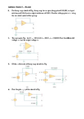
Problems Chapter 4 - Transistor
1. Transistor in the circuit has β=100 and VBE=0.7V at ic=1mA. Design the circuit so that the
current 2mA flows through the collector and a voltage of +5 appear at the collector
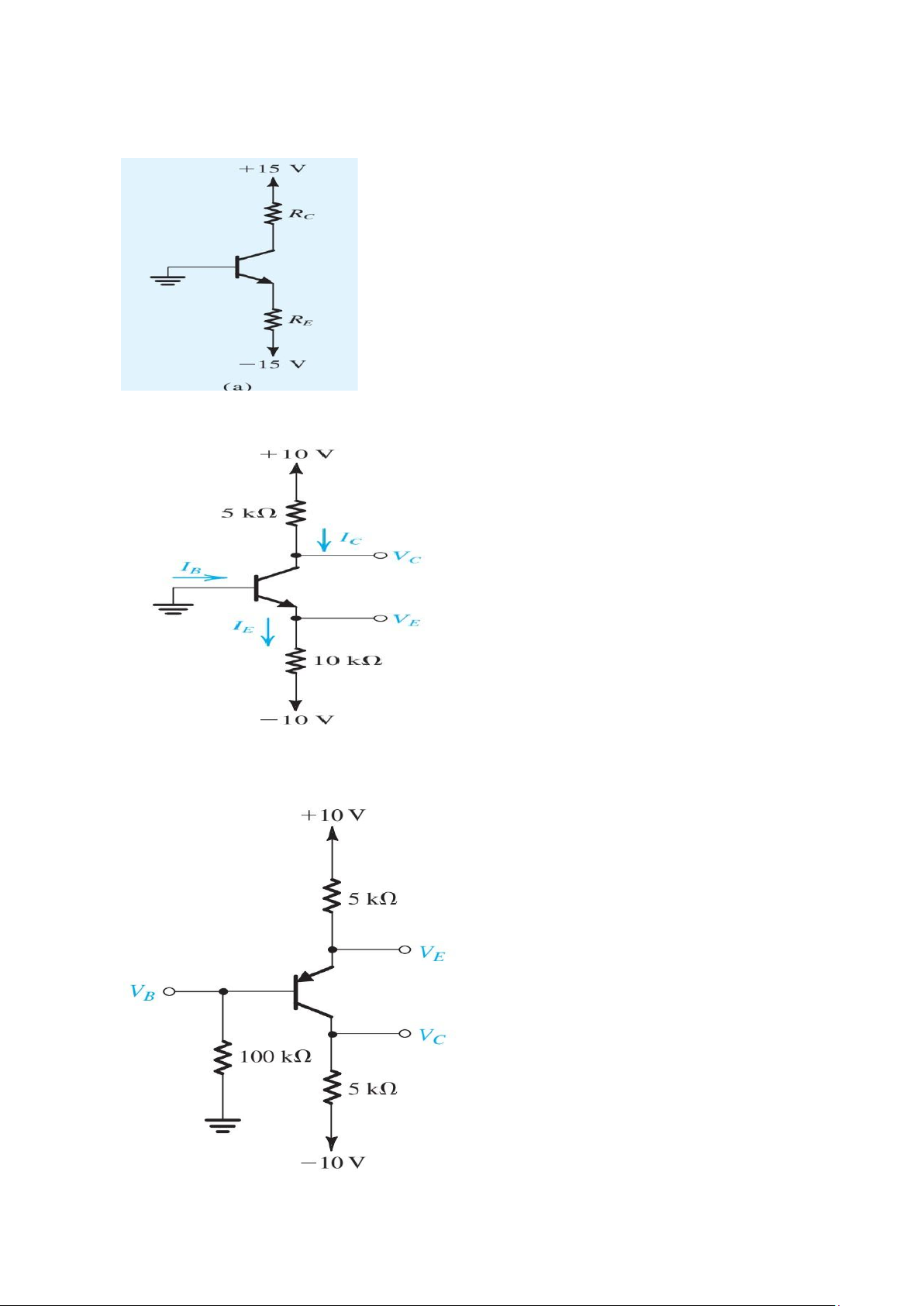
2. In the circuit shown in Fig. E6.13, the voltage at the emitter was measured and found to be
–0.7 V. If β = 50, find IE, IB, IC, and VC
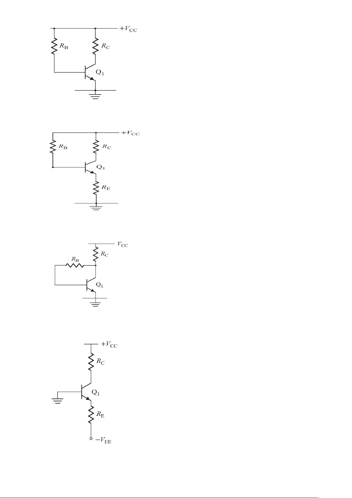
3. In the circuit shown in Fig. E6.14, measurement indicates VB to be +1.0 V and VE to be
+1.7 V.What are α and β for this transistor? What voltage VC do you expect at the collector? 4. lOMoAR cPSD| 58707906
5. For the transistor circuit of Fig, find IB, VCE and v0 Take β= 200, VBE = 0.7V
6. For the transistor circuit shown in Fig. find IB and VCE Let and β= 100, VBE =0.7V
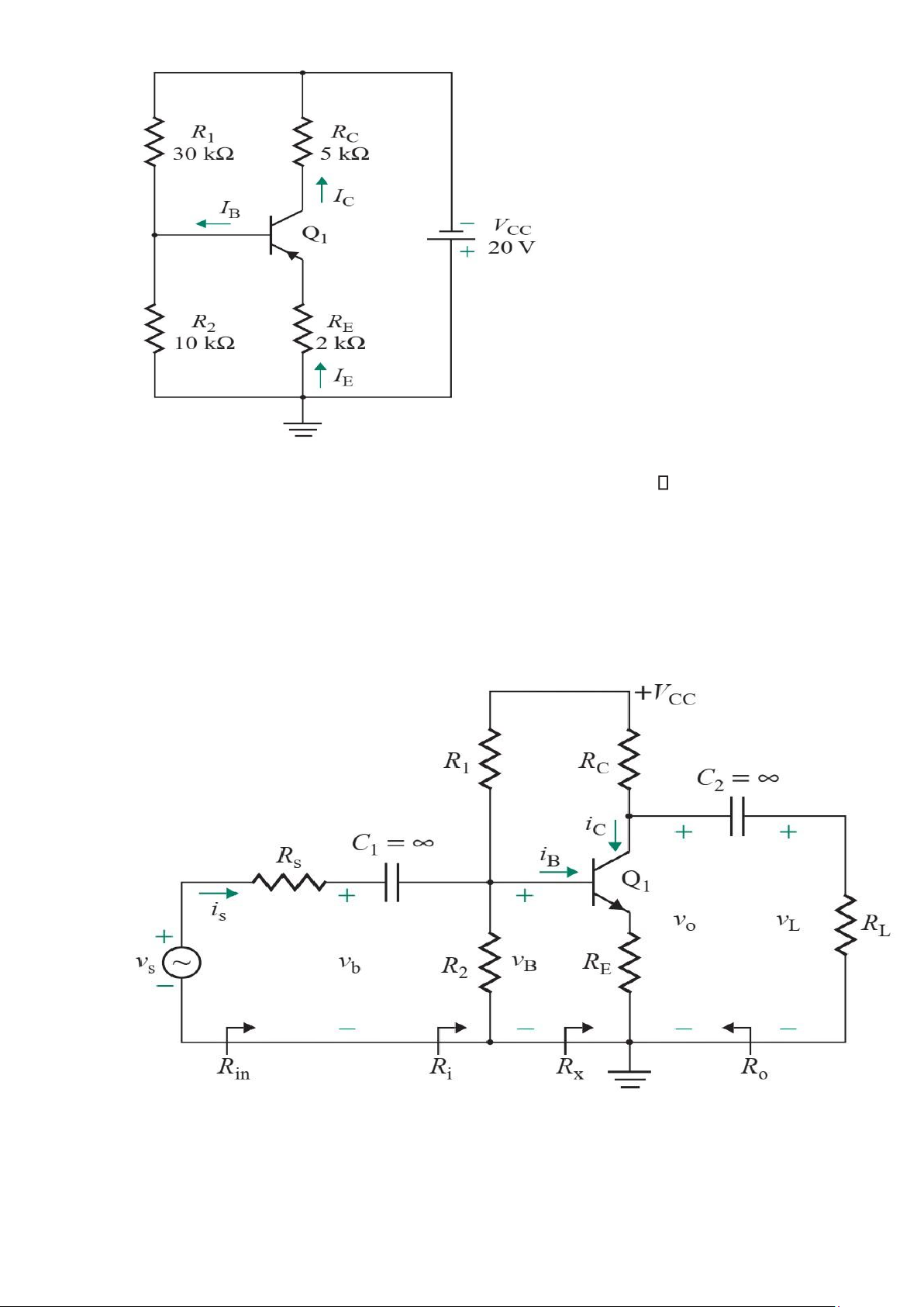
7. Calculate vs for the transistor in Fig. given that v0= 4 V, β= 150, VBE =0.7 V.
8. The parameters of an npn transistor are αF = 0.9934 and IB = 25 A. Determine (a) the
forward current gain βF, (b) the collector current iC, and (c) the emitter current iE.
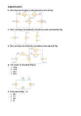
9. The parameters of the transistor in Fig. P8.13 are β=150, VBE = 0.7V and VCE(sat) = 0.3V. If
RC = 1.5KΩ, determine the critical value of RB so that the transistor operates (a) in the
active (amplifier) region and (b) in the saturation region lOMoAR cPSD| 58707906
10. The parameters of the transistor in Fig. P8.14 are β=150, VBE=0.7V and VCE(sat)= 0.3V. If
RC=1.5KΩ and RE=500Ω , determine the critical value of RB so that the transistor operates
(a) in the active (amplifier) region and (b) in the saturation region
11. The parameters of the transistor in Fig. P8.15 are β=150, VBE=0.7V and VCE(sat)= 0.3V. If
RC=1.5KΩ, determine the critical value of RB so that the transistor operates (a) in the
active (amplifier) region and (b) in the saturation region
12. The parameters of the transistor in Fig. P8.16 are β=150, VBE=0.7V, and VCE(sat)=0.3V. If
VCC=12V , VEE=12V and RC=1.5KΩ , determine (a) the base current IB, (b) the collector
current IC, and (c) the C-E voltage VCE. lOMoAR cPSD| 58707906
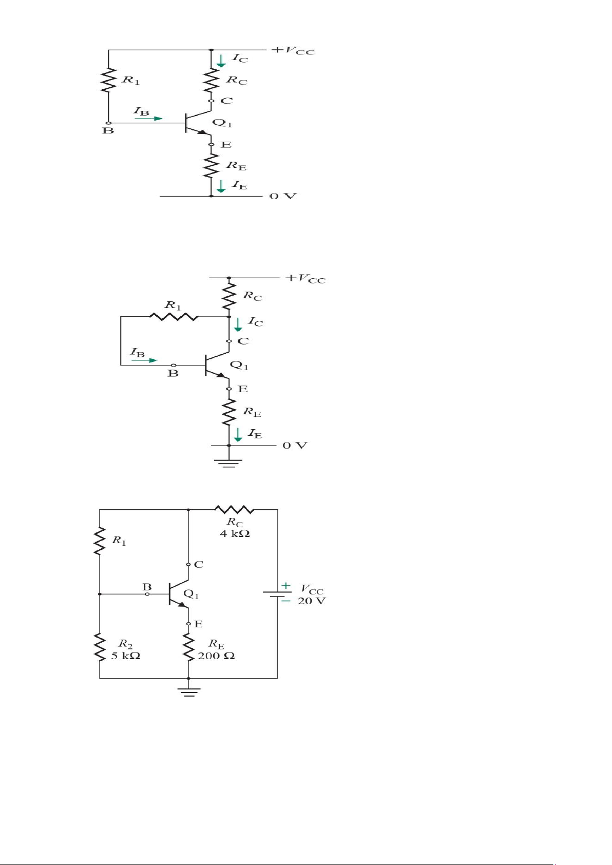
13. The parameters of the transistor in Fig. P8.17 are β=150, VBE=0.7V, and VCE(sat)=0.3V. If
VCC=12V , RB=200KΩ and RC=1.5KΩ , RE=500Ω determine (a) the base current IB, (b)
the collector current IC, and (c) the C-E voltage VCE.
14. The parameters of the transistor in Fig. P8.18 are β=150, VBE=0.7V, and VCE(sat)=0.3V. If
VCC=15V , VB=5V, RB=200KΩ and RC=1.5KΩ , RE=500Ω determine (a) the base current
IB, (b) the collector current IC, and (c) the C-E voltage VCE.
15. The parameters of the pnp BJT circuit in Fig. P8.19 are RC =10 kΩ, RE =1kΩ, VCC =15
V, VEE =5 V, VEB =0.6 V, and α=F 0.992. Calculate IB, IC, IE, VCE, and VCB at the Qpoint
16. The parameters of the npn transistor circuit in Fig. P8.20 are R1 =100 kΩ, RC =1kΩ, RE
=200Ω , VBE = 0.7V, and VCC=12 V.
a. Calculate IB, IC, IE, and VCE at the operating point if βF =50 and if βF =250. b. Repeat
part (a) if RE =0 lOMoAR cPSD| 58707906
17. The parameters of the transistor circuit in Fig. P8.21 are R1 =10 kΩ, RC 1 =kΩ, RE =200Ω
, VBE =0.7V, and VCC =12 V.
a. Calculate IB, IC, IE, and VCE at the Q-point if βF =50 and if β F =250.
b. Repeat part (a) if RE =0
18. The npn transistor circuit of Fig. P8.23 has VBE =0.5 V and βF =80. Determine the value
of R1 that gives IC =4 mA and the corresponding value of VCE
19. The pnp transistor circuit of Fig. P8.24 has βF =100 and VEB =0.7 V. Calculate IC and VCE lOMoAR cPSD| 58707906
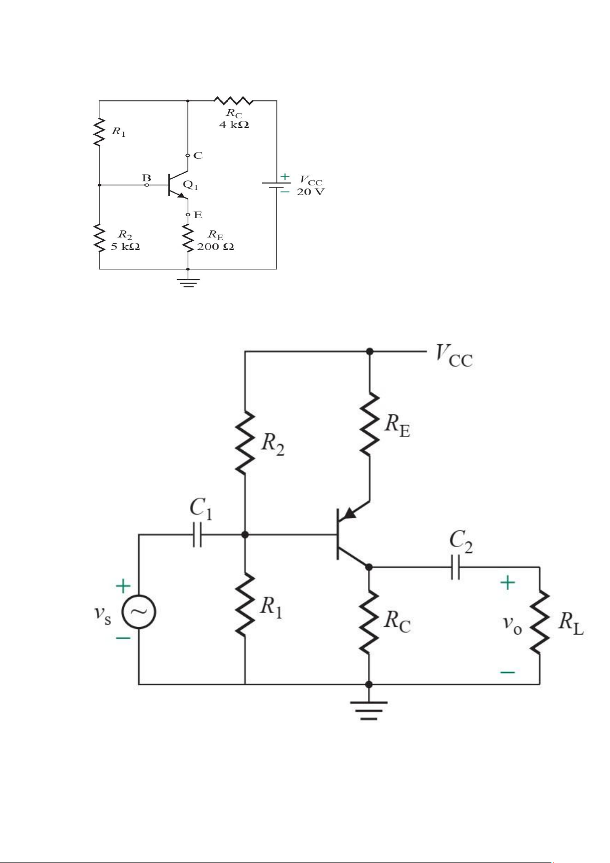
20. The parameters of the amplifier circuit in Fig. P8.25 are VCC =5 V, RC =500Ω, R1 =6.5 k
Ω, R2 =2.5 k Ω, RE =450 Ω, Rs =500 Ω, RL =5 k Ω, and C1 =C2= . Assume βF =100 and VA =200 V
a. Find the Q-point defined by IB, IC, and VCE.
b. Calculate the small-signal parameters gm, r, and ro of the transistor.
c. Calculate the input resistance Rin vs ⁄ is, the no-load voltage gain Avo vo ⁄ vb, the
output resistance Ro, the overall voltage gain Av vL ⁄ vs, the current gain Ai io ⁄ is, and the power gain Ap.
d. Use PSpice/SPICE to plot the instantaneous values of vL, vC, vB, iC, and iB.
21. The BJT amplifier of Fig. 8.23 has R1 =5.5 kΩ, R2 1.5 =kΩ, RC =1.5 kΩ, RE =150Ω , RL
=5 kΩ, Rs =200Ω , and VCC =18 V. Assume βF= 100 and VA =200 V
a. Find the Q-point defined by IB, IC, and VCE.
b. Calculate the small-signal parameters gm, r, and ro of the transistor.
c. Calculate the input resistance Rin vs ⁄ is, the no-load voltage gain Avo vo ⁄ vb, the lOMoAR cPSD| 58707906
output resistance Ro, the overall voltage gain Av vL ⁄ vs, the current gain Ai io ⁄ is, and the power gain Ap.
d. Use PSpice/SPICE to plot the instantaneous values of vL, vC, vB, iC, and iB
22. The emitter follower of Fig. P8.31 has R1 =100KΩ , R2 =150 KΩ , RE =750 Ω, RL =20
KΩ , Rs =200 Ω, VCC =15 V, and VBE= 0.7 V. Assume that βF =100 and VA =200 V 23.
Tài liệu liên quan:
-
Problems Chapter 1 Contents | Môn Điện tử căn bản - Đại học Sư phạm Kỹ thuật Thành phố Hồ Chí Minh
114 57 -
Problems Chapter 9 Contents | Môn Điện tử căn bản - Đại học Sư phạm Kỹ thuật Thành phố Hồ Chí Minh
113 57 -
Problems Chapter 5 Contents | Môn Điện tử căn bản - Đại học Sư phạm Kỹ thuật Thành phố Hồ Chí Minh
107 54 -
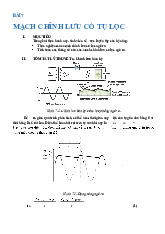
Bài 7: Mạch Chỉnh Lưu Có Tụ Lọc | Môn Điện tử căn bản - Đại học Sư phạm Kỹ thuật Thành phố Hồ Chí Minh
174 87 -
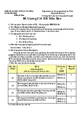
Đề Cương Chi Tiết Môn Điện tử căn bản | Đại học Sư phạm Kỹ thuật Thành phố Hồ Chí Minh
141 71