VLSI Design Mini Project Report: OpenLane EC383 Analysis môn Thiết kế hệ thống VLSI | Học viện Công Nghệ Bưu Chính Viễn Thông
This project explores the higly customizable Pi- coRV32 and explores its various configurations. Tài liệu được sưu tầm gồm 17 trang, giúp các bạn nắm vững kiến thức, rèn luyện kỹ năng và đạt được kết quả tốt trong học tập. Mời các bạn đón xem!
Môn: Thiết kế hệ thống VLSI 6 tài liệu
Trường: Học viện Công Nghệ Bưu Chính Viễn Thông 1.8 K tài liệu
Tác giả:


Preview text:
lOMoAR cPSD| 58815430
RISC-V based micro-controller using OpenLane
EC383 Mini Project in VLSI Design Final project report
Electronics and Communication Engineering
National Institute of Technology April 8, 2022
Kruti Deepan Panda, 191EC126.
Rahul Magesh, 191EC145. Abstract 2 Literature survey
This project explores the higly customizable Pi- 1. OpenLane tutorials
coRV32 and explores its various configurations. We • https://github.com/
have tried running the base core enabled with PCPI,
AXI version of the core with PCPI and multiply The-OpenROAD-Project/OpenLane
module enabled, AXI version of the core with PCPI,
• https://inst.eecs.berkeley.edu/
multiply module, 2 clock cylce ALU and 2 clock cycle ~cs250/fa20/labs/lab1/
compare enabled. We tried to fix errors and STA • https://www.researchgate.
violations that occured during our runs and tried to net/publication/355051535_
determine the highest possible clock frequenct the IBTIDA_Fully_open-source_
core can run in the most stable manner possible.
ASIC_implementation_of_ Chisel- generated_System_on_ a_Chip
• https://openlane.readthedocs. 1 Introduction io/en/latest/docs/source/
In this project we explore the OpenLane flow [3] advanced_readme.html
and the various combinations of the PicoRV32 • https://openlane-docs.
processor [5] to add additional functionality to it.
readthedocs.io/en/rtd-develop/ doc/OpenLANE_commands.html 2. Understanding IR drop
• https://vlsi-backend-adventure. 3.1 PicoRV32 com/ir_analysis.html 3. Antenna Diodes
• https://www.edn.com/ antenna-violations-resolved- using-new-method/ 4. Congestion fixes Base core
• https://lmr.fi/int/ congestion-in-vlsi-physical- design-flow/
The PicoRV32 is a higly customizable core by 5. Fixing hold violations
YosysHQ.The PicoRV32 is a small core in terms of • https://vlsiuniverse.
area but has high configurability. It can be
blogspot.com/2017/02/ fixing-hold-
configured as RV32E, RV32I, RV32IC, RV32IM, or violations.html?m=1
RV32IMC core, and optionally contains a built-in
interrupt controller. [5] On top of that the core
supports multiple memory interfaces. The core 6. Understanding routing
exists in three variations: picorv32, picorv32_axi
and picorv32_wb. The first provides a simple native
• https://www.ifte.de/books/eda/
memory interface, that is easy to use in simple chap5.pdf
environments. picorv32_axi provides an AXI-4 Lite
Master [4] interface that can easily be integrated
with existing systems that are already using the AXI
standard. picorv32_wb provides a Wishbone 3 Project details master interface [5].
In this section we elaborate on the various as- pects
The core also includes a separate core pi- of our project.
corv32_axi_adapter is provided to bridge between
the native memory interface and AXI4. This core can
be used to create custom cores that include one or
more PicoRV32 cores together with local RAM, ROM, and memory-mapped peripherals,
communicating with each other using the native
interface, and communicating with the outside world via AXI4. [5]
is set as well [5]. By default it is 0. Axi Interface Enabled
Wishbone interface enabled
PicoRV32 comes with internal verilog param-
eters which can be modified to generate our de-
sired core. These internal parameters can be
modified to implement additional features of the
base core. When a parameter is set the
corresponding logic or modules is generated using
the generate keyword in verilog. Some parameters are explained below. 3.1.1 COMPRESSED_ISA
This enables support for the RISC-V Compressed
Instruction Set [5]. By default it is 0. 3.1.2 ENABLE_PCPI
Set this to 1 to enable the Pico CoProcessor
Interface (PCPI) [5]. By default it is 0. 3.1.3 ENABLE_MUL
This parameter internally enables PCPI and in-
stantiates the picorv32_pcpi_mul core that im-
plements the MUL[H[SU|U]] instructions. The external PCPI interface only becomes functional
when ENABLE_PCPI is set as well [5]. By default it is 0. 3.1.4 ENABLE_FAST_MUL
This parameter internally enables PCPI and instantiates
the picorv32_pcpi_fast_mul core
that implements the MUL[H[SU|U]]
instructions. The external PCPI interface only be-
comes functional when ENABLE_PCPI This
3.1.5 ENABLE_DIV mentioned above. PCPI helps adding additional functionality to the core easier
parameter pro- vided they are non-branching internally enables PCPI instructions.
and in- stantiates the picorv32_pcpi_div core that
im- plements the DIV[U]/REM[U] instructions.
The external PCPI interface only
becomes functional when ENABLE_PCPI is set as well [5].
3.1.6 TWO_CYCLE_COMPARE
This relaxes the longest data path a bit by
adding an additional FF When an unsupported instruction
is stage at the cost of found by PicoRV32 occurs it asserts
adding an additional pcpi_valid. The un- sopported instruction
clock cycle delay to the is sent to pcpi_insn for the co-
processor conditional branch to recognise it. The decoded values of instructions. By default registers is
made available through it is 0 [5]. pcpi_rs1 and pcpi_rs2 and its output can be
Note: Enabling this parameter will be most ef- fective
when retiming (aka "register
balancing") is enabled in the synthesis flow. 3.1.7 TWO_CYCLE_ALU
This adds an additional FF stage
in the ALU data path, improving timing at the cost of an
additional clock cycle for all
instructions that use the ALU. By default it is 0 [5].
Note: Enabling this parameter will be most ef- fective when retiming (aka "register balancing") is enabled in the synthesis flow. 3.2 Pico Co- Processor Interface (PCPI) The thing that makes PicoRV32
ideal for use in microcontrollers
is its Pico Co-Processor Interface
(PCPI) feature. The PCPI is an interface that can be enabled by changing verilog param- eters as
sent to pcpi_rd. The pcpi_ready needs to as- serted the multi- ple variations of optimizations is better suited for our use case.
when the execution of the instruction is over.
When no external PCPI core acknowledges the 3.3.2 Floorplanning
instruction within 16 clock cycles, then an illegal Chip Floorplanning is the arrangement of logi- cal block, library cells, pins
instruction exception is raised and the respective on silicon chip. It makes sure that every module has been assigned an
interrupt handler is called. A PCPI core that needs appropriate area and aspect ratio, every pin of the module has
more than a couple of cycles to execute an connection with other mod- ules or periphery of the chip and modules
instruction, should assert pcpi_wait as soon as the are arranged in a way such that it consumes lesser area on a chip
instruction has been decoded successfully and keep [2].
it asserted until it asserts pcpi_ready. This will We also have power planning. Power planning is a step in which power
prevent the PicoRV32 core from raising an illegal grid network is cre- ated to distribute power to each part of the design instruction exception. [5]
equally. This step deals with the un- wanted voltage drop and ground
bounce. Steady state IR Drop is caused by the resistance of the metal 3.3 Stages of the Flow
wires comprising the power distribution network. By reducing the 3.3.1 Synthesis
voltage difference be- tween local power and ground, steady-state IR
Drop reduces both the speed and noise immunity of the local cells and
This is the very first stage of the flow. Most of the macros [2].
initial preparation happens in this stage. OpenLane 3.3.3 Placement
first goes through the mentioned source files and
looks through it for optimising it. Initially it tries to Placement is the step when it is actually decided where the different cells
remove dead code. Dead code analysis involves will be placed on the
unnecessary wires and modules that has never
been used by any module. Dead code analysis is
important as it helps OpenLane to focus on only the
relevant verilog code. At the end of the synthesis
stage the verilog file is replaced by optimized wires
and standard mod- ules by Skywater. We can also
run synthesis exploration and understand which of
die. Placement does not just place the
OpenLane supports running multithreaded runs for
standard cells available in the routing.
synthesized netlist. It also optimizes the design, thereby removing any
timing violations created due to
3.4 config.tcl parameters the relative placement on die [2].
In this section, we elaborate on the config pa-
rameters we tampered with for optimizing our
OpenLane does placement in two stages - design. • Global Placement • Detailed Placement
3.3.4 Clock Tree Synthesis Clock Tree
Synthesis(CTS) is a process which
makes sure that the clock gets
distributed evenly to all sequential
elements in a design. The goal of CTS
is to minimize the clock latency and
skew [2]. There are several CTS techniques like: • H - Tree • X - Tree • Fish bone
In OpenLANE, clock tree synthesis is
carried out using TritonCTS tool. CTS should always be done after the floorplanning
and placement as the CTS is carried
out on a placement.def file that is
created during placement stage [2]. 3.3.5 Routing OpenLANE uses TritonRoute, an open source router for modern industrial designs. The router consists of
several main building blocks, including
pin access analysis, track assignment,
initial detailed routing, search and repair, and a DRC engine. The
routing process is implemented in two stages: • Global Routing - Routing guides are gener- ated for interconnects.
• Detailed Routing - Tracks are generated in- teratively.
TritonRoute 14 ensures there are no
DRC viola- tions after routing. 3.4.1 CLOCK_PERIOD
This parameter is used to set the time period(in
nanoseconds) of the clock signal used for timing the
circuit. Note that we try reducing this value as much
as possible for a faster design. Default Value = "24.0" Value used = "20" 3.4.2 CLOCK_PORT
The name of the design’s clock port used in Static
Timing Analysis. Value = "clk". 3.4.3 FP_CORE_UTIL
This parameter is used to control the core uti-
lization percentage. Note that having an overly high
value of core utilisation in floor planning leads to routing congestion. Default Value = "50" Value used = "45" 3.4.4 ROUTING_CORES
Specifies the number of threads to be used in
TritonRoute. Can be overriden via environment
variable [3]. Default Value = "2" Value used = "8"
3.4.5 PL_TARGET_DENSITY
The desired placement density of cells. It reflects
how spread the cells would be on the core area. This
value is chosen around 1-5% higher than FP_CORE_UTIL. Default Value = "0.55" Value used = "0.47" 3.4.6 CLK_BUFFER
This is the root clock buffer of the clock tree. Default value = "sky130_fd_sc_hd clkbuf_16"
Note that _16 refers to the drive strength of the
clock buffer. We have decreased the drive strength
to 8 in our design to help us deal with hold timing violations. Value used = "sky130_fd_sc_hd clkbuf_4"
3.4.7 FP_IO_MIN_DISTANCE
The minimum distance between the IO pads in
microns. Default Value = "3" Value used = "3" lOMoAR cPSD| 58815430
3.4.8 PL_ROUTABILITY_DRIVEN
pins and smartly inserting needed diodes
inside the design, 5 = a mix of strategy Specifies whether the
2 and 4. Default Value = "3" placer should use Value used = "3"
routabil- ity driven Note that diode insertion can help us placement. 0 = false, 1 deal with pin violations = true [3]. Def caused by
antenna errors, however this will be at
the cost of additional delay and leakage ault Valu e =
power consumption. We have set the
value to 4 during trial 6 while trying to reduce the no. of pin violations due to "0" antenna error. Valu e use
3.4.11 SYNTH_MAX_FANOUT d = "0"
The max load that the output ports can
drive. Default Value = "5" Value used = "6" 3.4.9 SYNTH_STRATEGY
This parameter sets the 3.4.12 GLB_RT_OVERFLOW_ITERS strategy for abc logic synthesis and
The maximum number of iterations technology mapping.
waiting for the overflow to reach the
Possible val- ues are desired value. DELAY/AREA 0-4/0-3; Default Value = "64" the
first part refers to Value Used = "55" the optimization target
of the synthesis 3.4.13 DRT_OPT_ITERS strategy (area vs.
delay) and the second Specifies the maximum number of one is an index. optimization iterations during Detailed Defaul Routing in Triton- Route. t Default Value = Value "64" Value Used = = "64" "AREA 0" Value used = "AREA 2" 3.4.10 DIOD E_INS ERTI ON_ STRA TEGY Specifies the insertion strategy of diodes to be used in the flow. 0 = No diode
insertion, 1 = Spray diodes, 2 =
insert fake diodes and replace them with real diodes if needed. 3= use FastRoute Antenna
Avoidance flow, 4 = Use Syl- vian’s Custom
Script for diode insertion on de- sign 3.4.14 SYNTH_CAP_LOAD
Default Value = "50" Value Used = 3.4.15 "99"
The capacitive load on the output ports in femtofarads. Default Value = "33.5" Value Used 4 Errors and Fixes = "50"
Note that we can increase the capacitance to fix Errors
hold violations by increasing delay.
• Routing congestion issues.
CTS_SINK_CLUSTERING_SIZ E
• [INFO GRT-0101] Running extra
iterations to remove overflow.
Specifies the maximum number of sinks per clus- INFO GRT-0103] Extra Run for hard ter. benchmark. Default Value = "25" Value Used = "60"
• [ERROR PPL-0072] Number of pins (409)
3.4.16 CTS_SINK_CLUSTERING_MAX_ exceed number of valid positions (384). DIAMETER
ERROR DPL-0036] Detailed placement failed.
Specifies maximum diameter (in micron) of sink Error: resizer.tcl, 79 DPL-0036 cluster. Used = "60"
Default Value = "50" Value • [ERROR DPL-0036] Detailed
placement failed. Error: resizer.tcl, 79 DPL-0036
3.4.17 PL_RESIZER_HOLD_MAX _ BUFFER_PERCENT 4.2 Fixes
Specifies a max number of buffers to insert to fix hold
violations. This number is calculated as a
percentage of the number of instances in the design.
Default Value = "50" Value Used = "99"
3.4.18 PL_RESIZER_SETUP_MA X_ BUFFER_PERCENT
Specifies a max number of buffers to insert to fix hold
violations. This number is calculated as a
percentage of the number of instances in the design.
Default Value = "50" Value Used = "99"
3.4.19 GLB_RESIZER_HOLD_MAX _ BUFFER_PERCENT
Specifies a max number of buffers to insert to
1. Fixes for routing congestion:
• Reduce placement utilization or in- crease area if set manually.
2. Fix for abnormally high routing time:
• Increase Area or fp_core_util 3. Fix for Insufficient pins:
• Increase placement utilization
4. Possible Fixes for hold violations:
• Increase Capacitance Increase core uti- lization percentage
• Decrease number of CTS sinks
• Decrease drive strength of buffers •
Increase no. of buffers placed
fix hold violations. This number isNote that most of the hold violation fixes
calculated as a percentage of the number of
reduce setup slack so there is a ideal balance instances in the design. between the two.
Default Value = "50" Value Used = "99"
5. Possible Fixes for setup violations: • Reduced clock speed
3.4.20 GLB_RESIZER_SETUP_MAX _ BUFFER_PERCENT • Decrease Capacitance
• Increase number of CTS sinks
Specifies a max number of buffers to insert to fix setup
violations. This number is calculated as a percentage
• Increase drive strength of buffers
of the number of instances in the design.
• Increase no. of buffers placed 5 Implementation
Since the usage of fastmul, axi, mul or div features increases
the peak memory usage during routing we focused
on improving the base core with pcpi enabled.
Our goal is to get the best possible clock frequency while
reducing all issues that may occur.
We decided to use sky130_fd_sc_hd
stan- dard cell library for its high density cells. [1]
This library enables higher routed gated density,
lower dynamic power consumption, comparable
timing and leakage power. As a trade-off it has lower
drive strength and does not support any drop in
replacement medium or high speed library.
Other features of it include -
• sky130_fd_sc_hd includes clockgating cells to
reduce active power 6 Results during non- sleep modes.
• Latches and flip-flops have scan equivalents to enable scan chain creation.
• Multi-voltage domain library cells are pro- vided. • Routed Gate Density is 160 kGates/mm2 or better. • Body Bias-able
Below is a table showing the PDK Synthesis Detailses: Implemented
exploration of base core propert VDD 1.8V
6.1 Outputs of interactive flow NMOS devices used sky130_fd_pr 8
6.1.1 .\flow.tcl − interactive nfet_01v
This command is used to enter the interactive8 mode of PMOS devices used sky130_fd_pr pfet_01v openlane. inverters, buffers 56
6.1.2 prep -design simple_risc AND, OR, NAND, 153
It prepares a run in openlane or loads a previously NOR
stopped run in order to proceed with it. It calls XOR, XNOR 8
trim_lib, prep_lefs, source_config, and other procs AND-OR-INV, OR-
to set all the needed environment variables. It has 115 AND-INV
similar flags to .\flow.tcl AND-OR, 132 ORAND Adders, Compara- 31 6.1.3 run_synthesis tors, Multiplexors
WeLatches andran 60the PicoRV32Runs yosys synthesis
on the current de- sign with the following configuration as well as OpenSTA timing analysis : lOMoAR cPSD| 58815430
on the generated netlist. The logs are pro- duced
under /<run_path</logs/synthesis/, the timing reports are under
/<run_path</reports/synthesis/, and the synthesized netlist under
/<run_path</results/synthesis/ We observed
that our worst slack for setup was
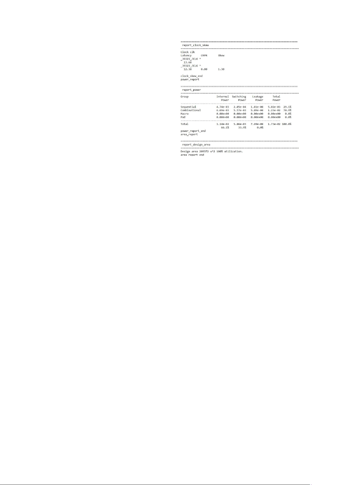
6.31 ns and worst slack for hold was 0.16 ns. =================
report_checks –slack_max -0.01 =================
No paths found. check_report_end check_slew =================
report_check_types -max_slew max_cap -max_fanout -violators 6.1.4 run_floorplan ================= =================
Runs init_floorplan, followed by one of the io max slew violation count 0 placement functions: if
::env(FP_PIN_ORDER_CFG) is defined then max fanout violation count place_io_ol is run; other- 0 max cap violation count wise, if 0 ::env(FP_CONTEXT_DEF) and =================
::env(FP_CONTEXT_LEF) are defined it runs check_slew_end tns_report
place_contextualized_io, if nothing of those is =================
defined then it runs the vanilla place_io. Then it runs report_tns
tap_decap_or on the processed design. Finally, ================= power grid tns 0.00 tns_report_end is generated utilizing wns_report ::env(VDD_NETS), ::env(GND_NETS), and =================
::env(SYNTH_USE_PG_PINS_DEFINES) if they are report_wns
defined, otherwise vanilla gen_pdn is used. The =================
resulting files are under /<run_path>/tmp/floorplan/ wns 0.00 wns_report_end and worst_slack
/<run_path>/results/floorplan/. =================
report_worst_slack -max (Setup)
At the end of floorplanning stage we saw that our =================
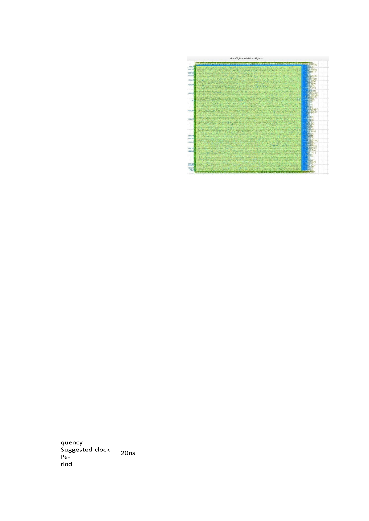
design had 409 pins; 21898 components and worst slack 6.31
162820 componentterminals; 22000 nets and =================
75187 connections; 500 endcaps; 6552 tapcells.
report_worst_slack -min (Hold)
An IR report helps us understand the robust- ness =================
worst slack 0.16 worst_slack_end
of our PDN (Power Delivery Network). An IR drop is clock_skew
defined as the average of the peak currents in the
power network multiplied by the effective
resistance of the power supply pads to the center of
the chip. Our IR report states that we have Worstcase voltage: 1.80e+00 V Average IR drop : 3.54e-09 V Worstcase IR drop: 5.10e-07 V 6.1.5 run_placement lOMoAR cPSD| 58815430 Runs global placement (global_placement or random_global_placeme nt based on the value of PL_RANDOM_GLB_PLACE MENT), lOMoAR cPSD| 58815430
then applies the optional optimizations ============= re- pair_wire_length followed by tns 0.00 tns_report_end wns_report
run_openPhySyn if enabled, then runs ============= the detailed placement (detailed_placement_or).
We had our worst slack for setup as 4.28 and worst
slack for hold as 0.17. After Openlane finished with
the resizing step, we had worst slack for setup as
5.59, and worst slack for hold is 0.20. All our timing
violations are dealt with here. Placement Analysis
——————————— total displacement 0.0 u average displacement 0.0 u max displacement 0.0 u original HPWL 1130746.5 u legalized HPWL 1146775.5 u delta HPWL 1 %
[INFO DPL-0020] Mirrored 378 instances [INFO DPL-0021] HPWL
before 1146775.5 u [INFO DPL-0022] HPWL after 1130746.5 u [INFO DPL-0023] HPWL delta -1.4 % 6.1.6 run_cts
Runs clock tree synthesis using the openroad app on
the processed design. The result- ing file is under
/<run_path>/results/cts/. It also generates a the
updated netlist using yosys and stores the results
under /<run_path>/results/synthesis and runs
yosys logic verification if enabled. Our design has -
• Total number of Clock Roots: 1.
• Total number of Buffers Inserted: 388.
• Total number of Clock Subnets: 388.
• Total number of Sinks: 2140. report_check_types -max_slew - max_cap -max_fanout -violators max slew violation count 0
max fanout violation count 0 max cap violation count 0 ============= check_slew_end tns_report ============= report_tns report_wns ort_ end wors t_sla ck ============= ============= wns 0.00
report_worst_slack -max (Setup) wns _rep ============= lOMoAR cPSD| 58815430 worst slack 5.55 =============
report_worst_slack -min (Hold) ============= wor st slac k 0.10 wors t_sla ck_e nd cloc k_sk ew
6.1.7 run_resizer_timing
This command resizes the layout to
optimize timing. It is used to fix
negative slack/timing violations. 6.1.8 run_routing Runs diode insertion based on the strategy, fol- lowed by global_routing, then ins_fill_cells,
detailed_routing, and finally SPEF extrac- tion on the
processed design. The result- ing file is under
/ <run_path>/results/routi ng/. It
also generates a pre_route netlist
6.1.9 run_antenna_check using yosys and stores the
Used to check for pin violations due to antenna results under
errors. Number of pins violated: 165 Number of
/<run_path>/results/synthesis, and it runs nets violated: 142
yosys logic verification if enabled. 6.1.10 run_magic Streams the final GDS and a mag view. The resulting file is under
/<run_path>/results/magic/. 6.1.11 run_magic_drc Runs a drc check on the CUR-
RENT_DEF. The resulting file is under
/<run_path>/logs/magic/magic.drc . 6.1.12 run_klayout Generates the klayout view. lOMoAR cPSD| 58815430
6.1.13 run_klayout_gds_xor
CVC: HI-Z Inputs: 0 CVC: Forward Bias Diodes: 0 CVC: NMOS
Generates xor between klayout and gds for Source vs Bulk: com- parison. 0 CVC: NMOS Gate vs Source: 0 CVC: NMOS Possible
6.1.14 run_magic_spice_export Leaks: 0 CVC:
Runs spice extractions on the processed PMOS Source vs Bulk: 0 CVC: design. Based on the value of PMOS Gate vs Source:
MAGIC_EXT_USE_GDS either the GDS or 0 CVC: PMOS Possible Leaks:
the DEF/LEF is used for the extraction. The 0 CVC: Overvoltage-VBG: 0 resulting file is under CVC: Overvoltage-VBS: 0
/<run_path>/results/magic/ . CVC: Overvoltage-VDS: 0 6.1.15 run_lvs CVC: Overvoltage-VGS: 0 CVC: Model errors: 0 Runs an lvs check between an CVC: Unexpected voltage : 0
extracted spice netlist EXT_NETLIST (so
run_magic_spice_export should be run CVC: Total: 0
before it.) and the current verilog
Usage Total: Time: 1 Memory: 88824 I/O: 80 netlist of the Swap: 0 pro- cessed Virtual net update/access design 913493/25695476 CVC: Log
CURRENT_NETLIST. The re- sulting file output to
is under /<run_path>/results/lvs/ and /openlane/designs/pic
/<run_path>/reports/lvs/. orv32_base/runs/
The LVS(Layout Version Schematic) RUN_2022.04.10_15.39.50/r
could be on the block/cell level or on ep CVC: End:
the device/transistor level, this is Sun Apr 10 17:00:43 2022
controlled by the extraction type set
by MAGIC_EXT_USE_GDS. If the GDS
is used in extraction then the LVS will
be run down to the device/transistor
level, otherwise it will be run on the
block/cell level which is the default behavior in OpenLANE. 6.1.16 run_lef_cvc
Runs CVC on the output spice, which is a
Circuit Validity Checker. Voltage aware ERC checker for CDL netlists. The output files exist under
<runpath>/results/cvc/. It is controlled by ::env(RUN_CVC) Power nets 81711 ! Checking overvoltage
errors ! Checking nmos possible leak errors:
! Checking pmos possible leak errors:
! Checking mos floating input errors: ! Checking expected values: CVC: Error Counts CVC: Fuse Problems: 0 CVC: Min Voltage Conflicts: 0 CVC: Max Voltage Conflicts: 0 CVC: Leaks: 0 CVC: LDD drain->source: 0 lOMoAR cPSD| 58815430
6.1.17 calc_total_runtime
6.1.19 generate_final_summary_r eport
Calculates the total runtime from the starting point Generates a final summary csv report of the most of the prep -design command.
important statistics and con- figurations in the run
as well as a man- ufacturability report with the
summary of DRC, LVS, and Antenna violations. This command is
6.1.22KLayout visualization 6.1.18 save_state Conclusions
Saves the current state of layout and netlist.
The Openlane flow of PicoRV32 reported hold
violations at lower clock periods which could be a
consequence of this processor being designed for
technologies with higher threshold voltage
6.1.20 check_timing_violations controlled by the flag
$::env(GENERATE_FINAL_SUMMARY_REPORTt)han sky130A.Majority of the flow runtime is
This command checks for any timing violations Wire count 18672 in the generated layouts. Wire bits 22310 public wires count 241 public wire bits 2984 Total Physical Cells 7052
6.1.21 Final summary report Suggested clock fre- 50 Mhz
Final summary report for AREA 2
utilized by routing, which is expected for a large Details Implemented design. VDD 1.8V Die 0.4878874905 Area in mm2 7 Future Work Number of vias 211597
Use of a better PDK with PDK with standard cells of Wire Length 1381424
higher drive strength can help improve our results Half Perimeter 1079684160
and reduce the number of buffers re- quired. wire length lOMoAR cPSD| 58815430 References
[1]Google. Skywater open source pdk. https:
//github.com/google/skywater-pdk, 2020.
[2]Shon Taware. Opensource physical de- sign.
https://github.com/ShonTaware/
OpenSource_Physical_Design, 2022. [3]The-OpenROAD-Project. Theopenroad- project/openlane:
Openlane is an auto- mated rtl to gdsii flow based on
several components including openroad, yosys,
magic, netgen, fault and custom method- ology
scripts for design exploration and optimization.
https://github.com/ The-OpenROAD- Project/OpenLane. [4]Xilinx. Amba axi4 interface protocol. https://www.edn.com/
antenna-violations-resolved-using-new-method/, 2015.
[5]Yosys. Picorv32 - a size-optimized risc- v cpu.
https://github.com/YosysHQ/ picorv32, 2022.
Tài liệu liên quan:
-
Lý thuyết Chương 1 đến 5 môn Thiết kế hệ thống VLSI | Học viện Công Nghệ Bưu Chính Viễn Thông
111 56 -

Giới hạn ôn thi: Chương 1-3 và bài tập thực hành môn Thiết kế hệ thống VLSI | Học viện Công Nghệ Bưu Chính Viễn Thông
93 47 -

Báo cáo Tìm hiểu cấu trúc và nguyên lí của 2 loại ổ cứng SSD và HDD môn Thiết kế hệ thống VLSI | Học viện Công Nghệ Bưu Chính Viễn Thông
86 43 -

Giáo trình môn Thiết kế hệ thống VLSI | Học viện Công Nghệ Bưu Chính Viễn Thông
167 84