Lecture 12: MOS Transistor Models môn mạch điện tử thông tin | Đại học Bách Khoa Hà Nội
Lecture 12: MOS Transistor Models môn mạch điện tử thông tin | Đại học Bách Khoa Hà Nội
Môn: Lý thuyết mạch điện 1 32 tài liệu
Trường: Đại học Bách Khoa Hà Nội 5.6 K tài liệu
Tác giả:


Preview text:
EECS 105 Fall 2003, Lecture 12 Lecture 12: MOS Transistor Models Prof. Niknejad Department of EECS
University of California, Berkeley
EECS 105 Fall 2003, Lecture 12 Prof. A. Niknejad Lecture Outline MOS Transistors (4.3 – 4.6)
– I-V curve (Square-Law Model)
– Small Signal Model (Linear Model) Department of EECS
University of California, Berkeley
EECS 105 Fall 2003, Lecture 12 Prof. A. Niknejad
Observed Behavior: I -V D GS IDS IDS VDS VGS VGS VT
Current zero for negative gate voltage
Current in transistor is very low until the gate
voltage crosses the threshold voltage of device
(same threshold voltage as MOS capacitor)
Current increases rapidly at first and then it finally
reaches a point where it simply increases linearly Department of EECS
University of California, Berkeley
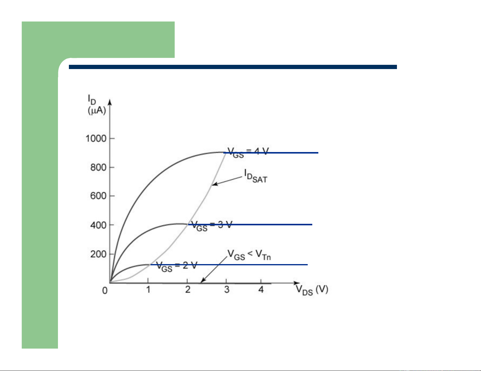
EECS 105 Fall 2003, Lecture 12 Prof. A. Niknejad
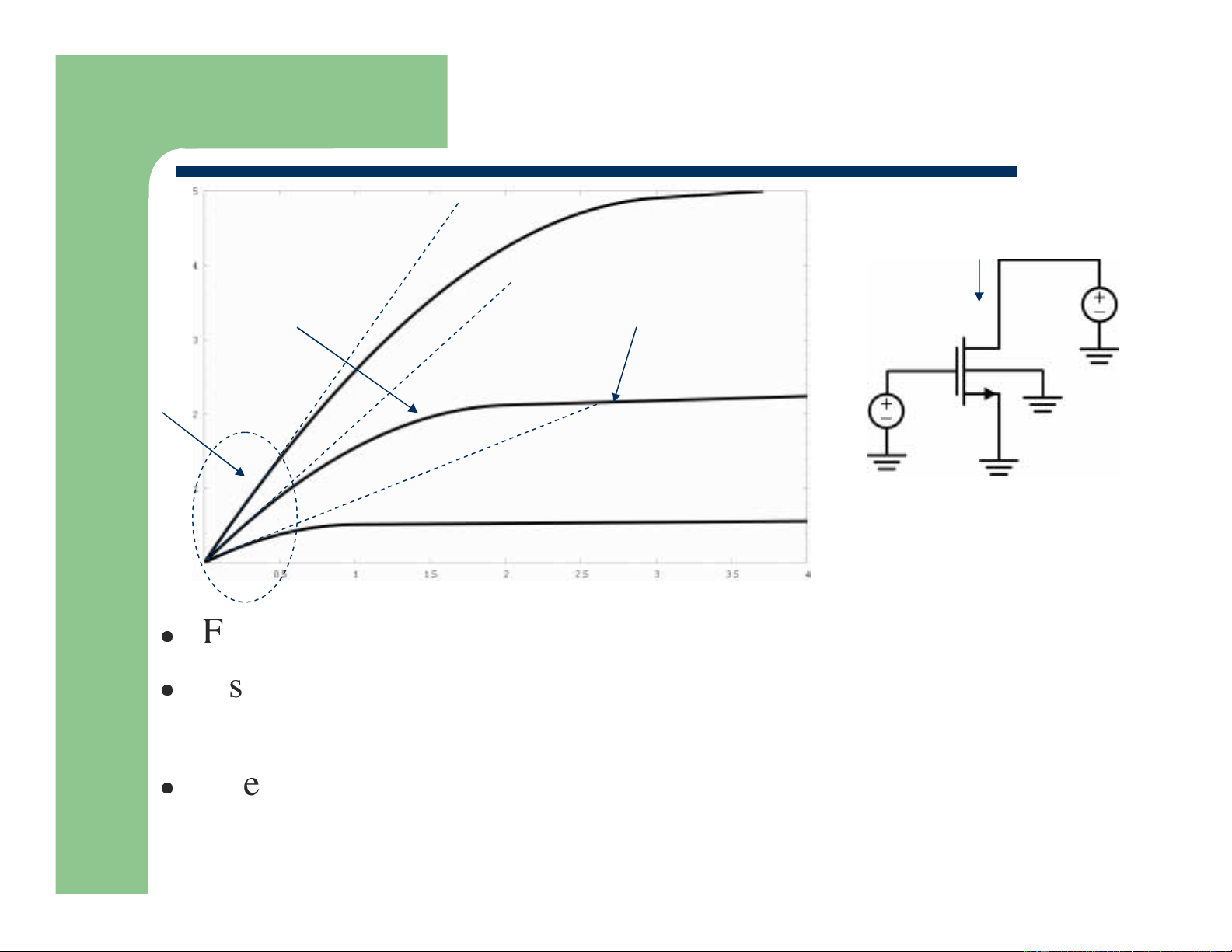
Observed Behavior: I -V D DS I / k V = 4V DS GS non-linear resistor region IDS “constant” current VDS V = 3V GS resistor region VGS V = 2V GS VDS
For low values of drain voltage, the device is like a resistor
As the voltage is increases, the resistance behaves non-linearly
and the rate of increase of current slows
Eventually the current stops growing and remains essentially constant (current source) Department of EECS
University of California, Berkeley
EECS 105 Fall 2003, Lecture 12 Prof. A. Niknejad
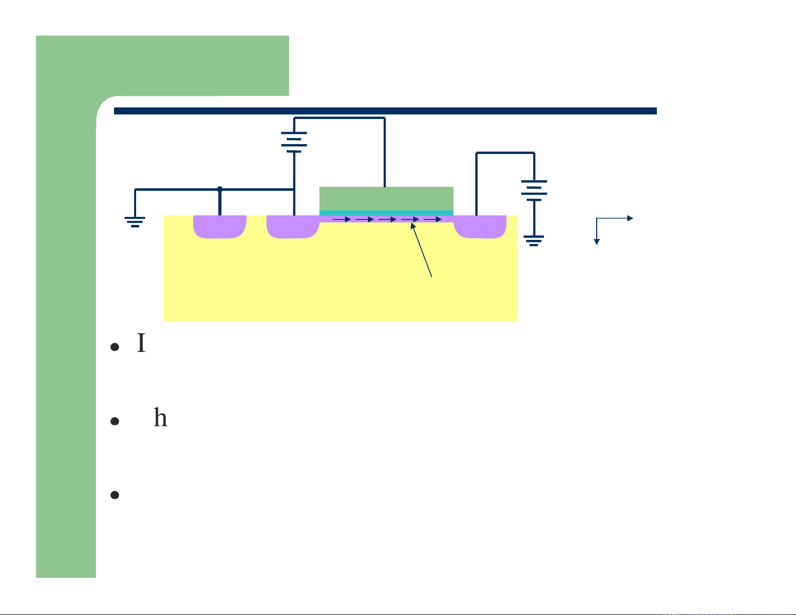
“Linear” Region Current V > V GS Tn G S V D ≈100mV DS y p+ n+ n+ x p-type Inversion layer NMOS “channel”
If the gate is biased above threshold, the surface is inverted
This inverted region forms a channel that connects the drain and gate
If a drain voltage is applied positive, electrons will flow from source to drain Department of EECS
University of California, Berkeley
EECS 105 Fall 2003, Lecture 12 Prof. A. Niknejad
MOSFET: Variable Resistor
Notice that in the linear region, the current is proportional to the voltage W I =
µ C (V −V )V DS n ox GS Tn DS L
Can define a voltage-dependent resistor V 1 L L DS R = = = R (V ) eq I
µ C (V −V ) GS W W DS n ox GS Tn
This is a nice variable resistor, electronically tunable! Department of EECS
University of California, Berkeley
EECS 105 Fall 2003, Lecture 12 Prof. A. Niknejad
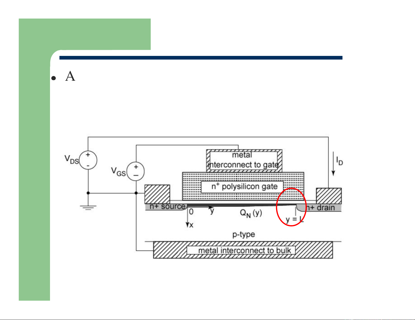
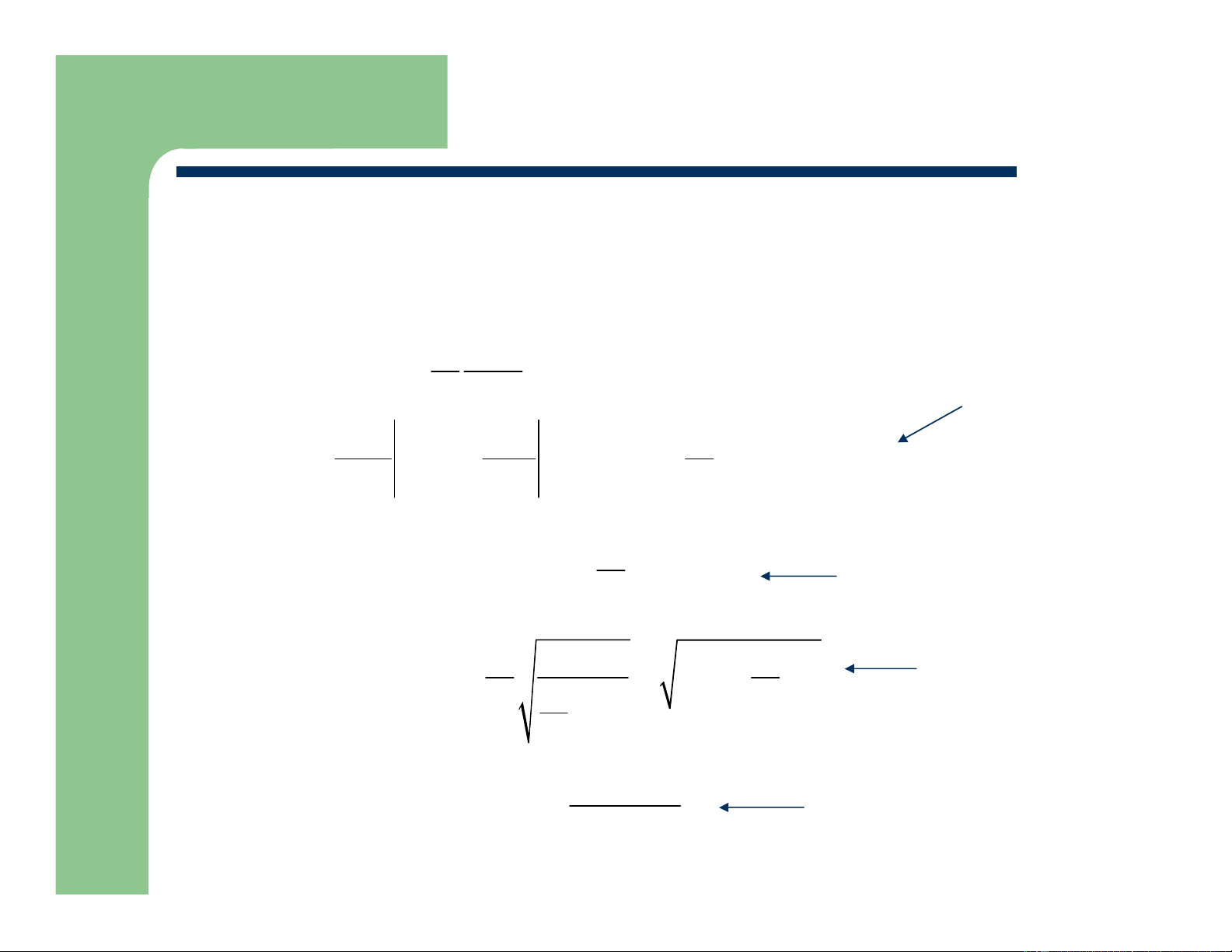
Finding I = f (V , V ) D GS DS
Approximate inversion charge Q (y): drain is N
higher than the source less charge at drain end of channel Department of EECS
University of California, Berkeley
EECS 105 Fall 2003, Lecture 12 Prof. A. Niknejad
Inversion Charge at Source/Drain
Q ( y) ≈ Q ( y = 0) + Q ( y = L) N N N
Q ( y = 0) = C − (V −V ) Q ( y N = L) = N ox GS Tn − C (V −V ) ox GD Tn = GD G V − S VDS Department of EECS
University of California, Berkeley
EECS 105 Fall 2003, Lecture 12 Prof. A. Niknejad
Average Inversion Charge Source End Drain End C (V
−V ) + C (V −V ) Q ( y) ox GS T ox GD T ≈ − N 2 C (V
−V ) + C (V −V −V ) Q ( y) ox GS T ox GS SD T ≈ − N 2 C (2V − 2V ) − C V V Q ( y) ox GS T ox SD ≈ − = −C ( DS V −V − ) N 2 ox GS T 2
Charge at drain end is lower since field is lower
Simple approximation: In reality we should
integrate the total charge minus the bulk depletion charge across the channel Department of EECS
University of California, Berkeley
EECS 105 Fall 2003, Lecture 12 Prof. A. Niknejad
Drift Velocity and Drain Current
“Long-channel” assumption: use mobility to find v µ V
v( y) = −µ E( y) ≈ −µ (− V ∆ / y ∆ ) n DS = n n L Substituting: V V DS I = W − vQ ≈ W µ C ( DS V −V − ) D N ox GS T L 2 W V I ≈ µC ( DS V −V − )V D ox GS T L 2 DS Inverted Parabolas Department of EECS
University of California, Berkeley
EECS 105 Fall 2003, Lecture 12 Prof. A. Niknejad
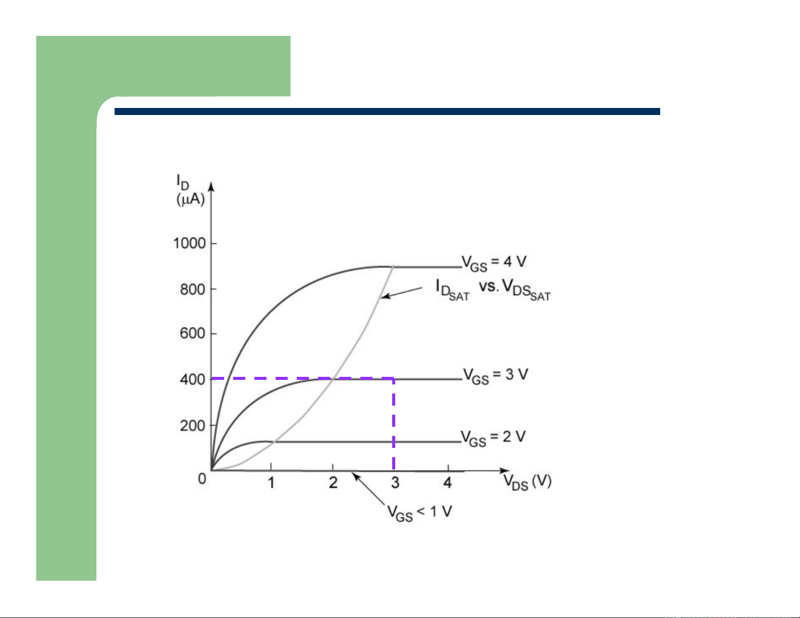
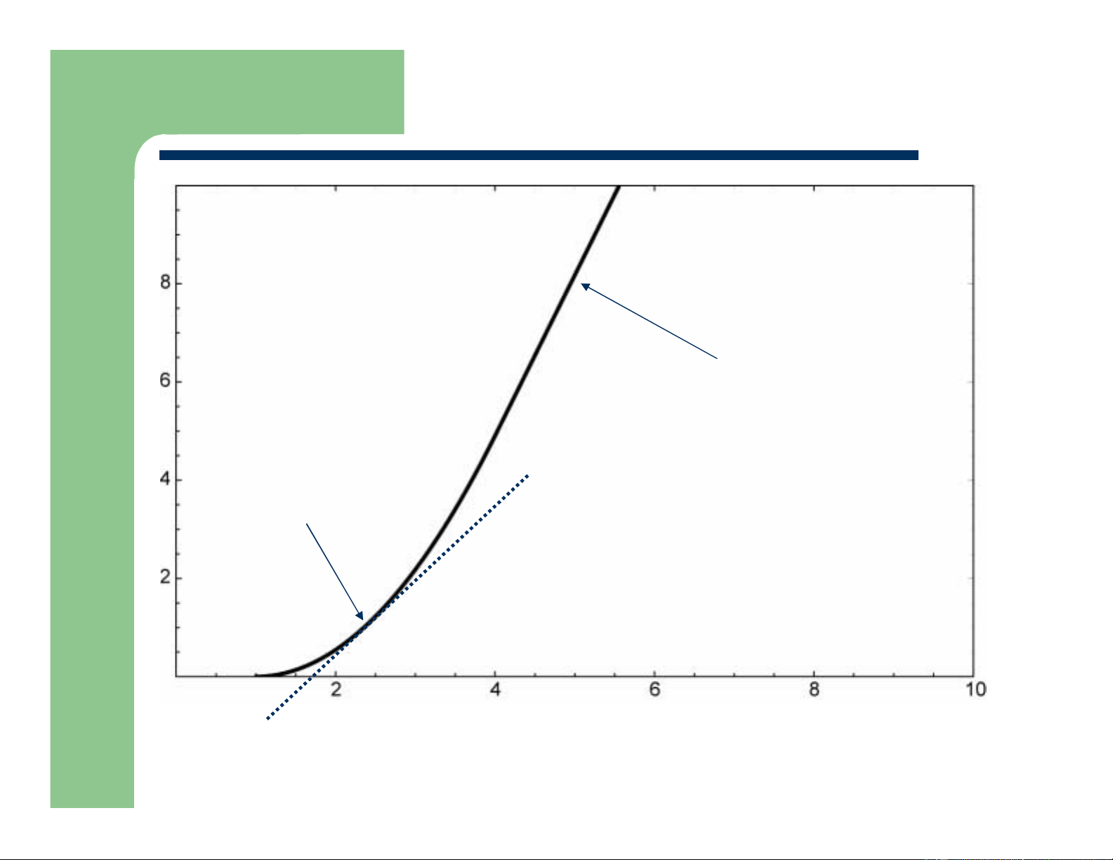
Square-Law Characteristics Boundary: what is I ? D,SAT TRIODE REGION SATURATION REGION Department of EECS
University of California, Berkeley
EECS 105 Fall 2003, Lecture 12 Prof. A. Niknejad The Saturation Region When V > V
– V , there isn’t any inversion DS GS Tn
charge at the drain … according to our simplistic model Why do curves flatten out? Department of EECS
University of California, Berkeley
EECS 105 Fall 2003, Lecture 12 Prof. A. Niknejad
Square-Law Current in Saturation
Current stays at maximum (where V = V – V = V ) DS GS Tn DS,SAT W V I = µC ( DS V −V − )V D ox GS T L 2 DS W V V I µ − = C ( GS T V −V − )(V −V ) DS ,sat ox GS T L 2 GS T W µCox 2 I = (V −V ) DS ,sat L 2 GS T
Measurement: I increases slightly with increasing V D DS
model with linear “fudge factor” W µCox 2 I = (V −V ) (1+ V λ ) DS ,sat L 2 GS T DS Department of EECS
University of California, Berkeley
EECS 105 Fall 2003, Lecture 12 Prof. A. Niknejad
Pinching the MOS Transistors V > V GS Tn G S V D DS p+ n+ n+ V −V GS Tn Depletion Region p-type NMOS Pinch-Off Point When V > V
, the channel is “pinched” off at drain end (hence the DS DS,sat name “pinch-off region”)
Drain mobile charge goes to zero (region is depleted), the remaining elecric
field is dropped across this high-field depletion region
As the drain voltage is increases further, the pinch off point moves back towards source
Channel Length Modulation: The effective channel length is thus reduced higher IDS Department of EECS
University of California, Berkeley
EECS 105 Fall 2003, Lecture 12 Prof. A. Niknejad Linear MOSFET Model
Channel (inversion) charge: neglect reduction at drain
Velocity saturation defines V = E L = constant DS,SAT sat - v / µ sat n Drain current: I = Wv − Q = W − (v )[ C − (V −V )], D,SAT N sat ox GS Tn
|E | = 104 V/cm, L = 0.12 µm V sat DS,SAT = 0.12 V! I
= v WC (V −V ) 1 ( + λ V ) D,SAT sat ox GS Tn n DS Department of EECS
University of California, Berkeley
EECS 105 Fall 2003, Lecture 12 Prof. A. Niknejad
Why Find an Incremental Model?
Signals of interest in analog ICs are often of the form: v (t) = V + v (t) GS GS gs Fixed Bias Point Small Signal
Direct substitution into i = f(v , v ) is D GS DS
tedious AND doesn’t include charge-storage
effects … pretty rough approximation Department of EECS
University of California, Berkeley
EECS 105 Fall 2003, Lecture 12 Prof. A. Niknejad Which Operating Region? V = 3V GS TRIODE V = 3V DS SAT OFF Department of EECS
University of California, Berkeley
EECS 105 Fall 2003, Lecture 12 Prof. A. Niknejad
Changing One Variable at a Time I / k DS Linear V = 3V Triode DS Square Law Region Saturation V = 1V T Region
Slope of Tangent: Incremental current increase VGS Assumption: V > V = V – V (square law) DS DS,SAT GS Tn Department of EECS
University of California, Berkeley
EECS 105 Fall 2003, Lecture 12 Prof. A. Niknejad
The Transconductance gm
Defined as the change in drain current due to a change in the
gate-source voltage, with everything else constant W µCox 2 I = (V −V ) (1+ V λ ) DS ,sat L 2 GS T DS ≈ 0 i ∆ i ∂ W D D g = = = µC (V −V )(1+ V λ ) m ox GS T DS v ∆ v ∂ L GS GS G V S , DS V GS V , DS V W g = µC (V −V ) m ox GS T L Gate Bias W 2I W DS g = µC = 2µC I Drain Current Bias m ox ox DS L W L µCox L 2IDS g = m Drain Current Bias and (V −V ) GS T Gate Bias Department of EECS
University of California, Berkeley
EECS 105 Fall 2003, Lecture 12 Prof. A. Niknejad
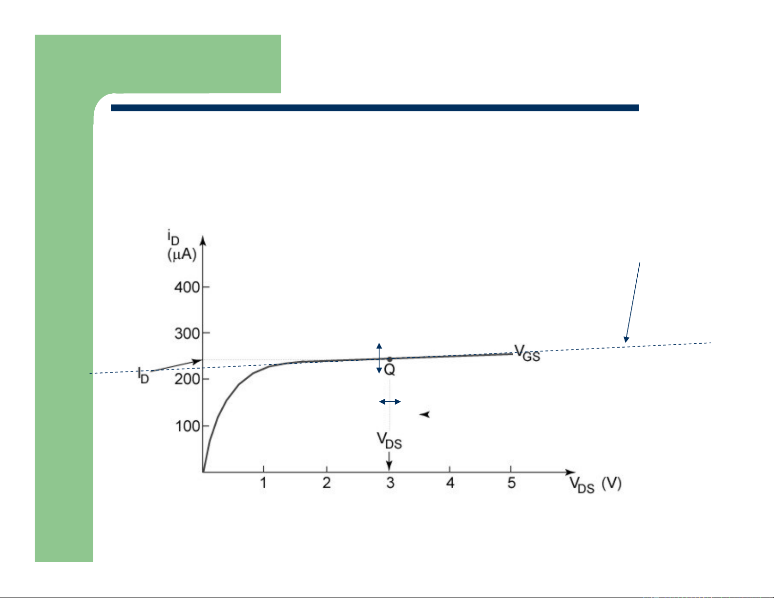
Output Resistance ro
Defined as the inverse of the change in drain current due
to a change in the drain-source voltage, with everything else constant Non-Zero Slope δ IDS δVDS Department of EECS
University of California, Berkeley
Tài liệu liên quan:
-

mmmmmmmmmmmmmmmmmmmmmmmmmmmmmmmmmmm
21 11 -
Bai tap on thi ve cac phan nang cao
24 12 -
Đáp án cho mạch điện, lý thuyết và thực hành | Lí thuyết mạch điện | Trường Đại học Bách khoa Hà Nội
31 16 -
Đồ án tốt nghiệp thiết kế hệ thống tự động điều chỉnh nhiệt độ trong thiết bị sấy hoa quả môn Lý thuyết mạch điện | Đại học Bách Khoa Hà Nội
31 16 -

IC-CAD Labs. Analog PartLect. 3 Cadence Layout Editor môn mạch điện tử thông tin | Đại học Bách Khoa Hà Nội
31 16