
Preview text:
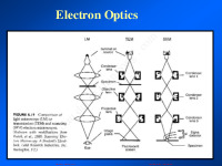
The Transmission Electron Microscope
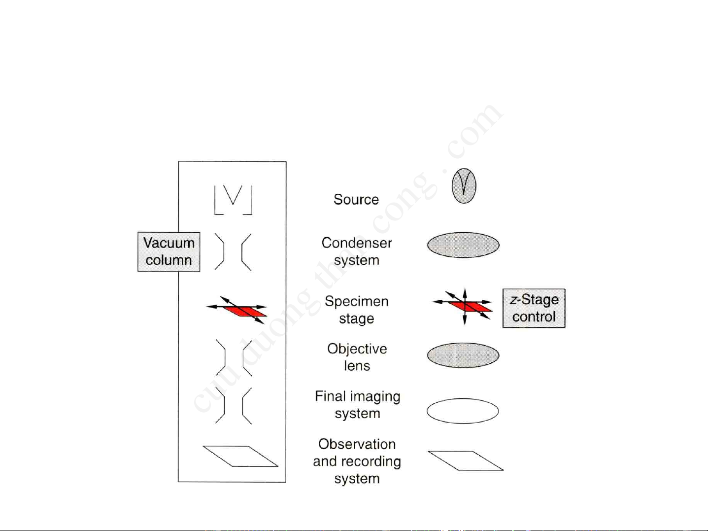
Analogous to transmission optical microscopy. apertures Also z, tilt, rotation cuu duong than cong . com
1 in 1020 electrons collected
<1 in 106 photons collected CuuDuongThanCong.com
https://fb.com/tailieudientucntt Components of TEMs
• Source - filament plus anode plates with applied accelerating voltage.
• Condensor Lenses - electromagnetic lenses
adjusted by lens currents not position.
• Specimen Stage - allows translations and tilts.
• Objective Lens - usually < 50x.
• Imaging System – multiple electromagnetic
lenses below the objective: set magnification,
focal plane (image vs. diffraction pattern).
• Observation - fluorescent screen, plate film or cuu duong than cong . com CCD camera. CuuDuongThanCong.com
https://fb.com/tailieudientucntt
The Scanning Electron Microscope
Uses secondary signals to obtain serial images: TEM SEM cuu duong than cong . com CuuDuongThanCong.com
https://fb.com/tailieudientucntt Components of SEMs
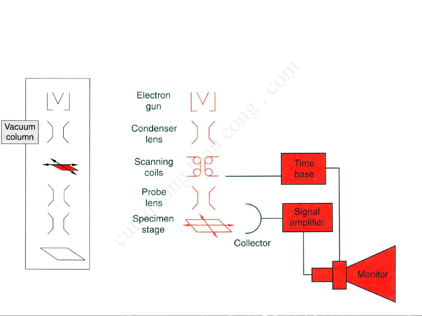
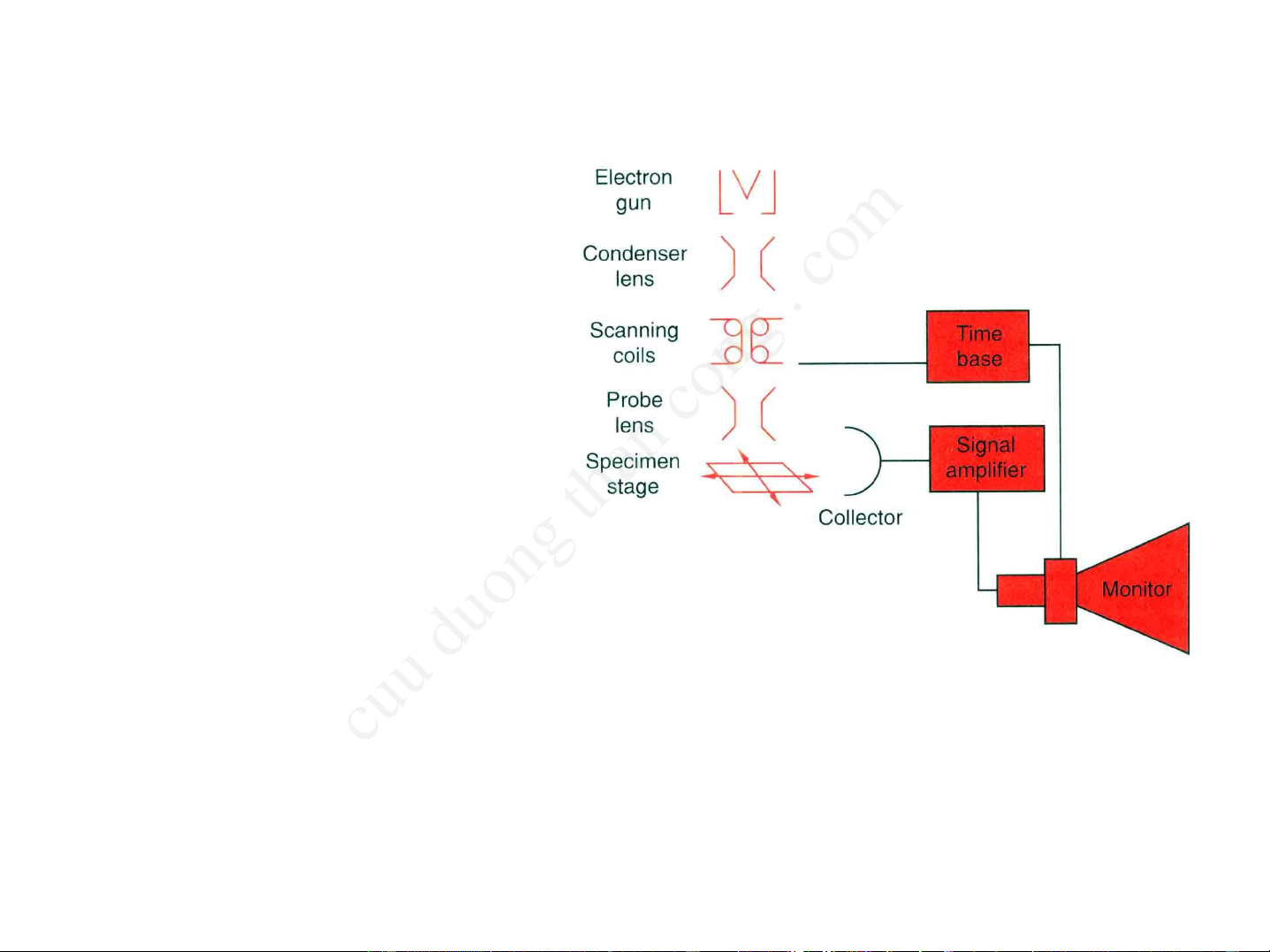
Source and condensor same as for TEM (lower V), but:
• Scanning Coils - raster the probe. • Probe Lens - lens forms a spot at the specimen surface. • Detector/Processing System
-Collects signals (X-rays, electrons etc.) as a
function of time (and thus position since probe scans with time).
-Gives digital “images” convenient for real-time cuu duong than cong . com
viewing, processing, and storage. CuuDuongThanCong.com
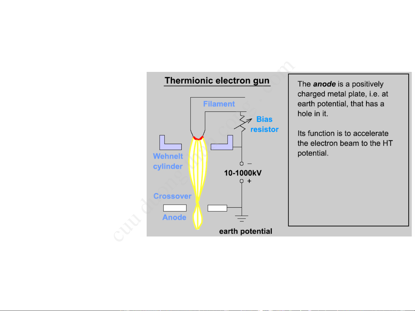
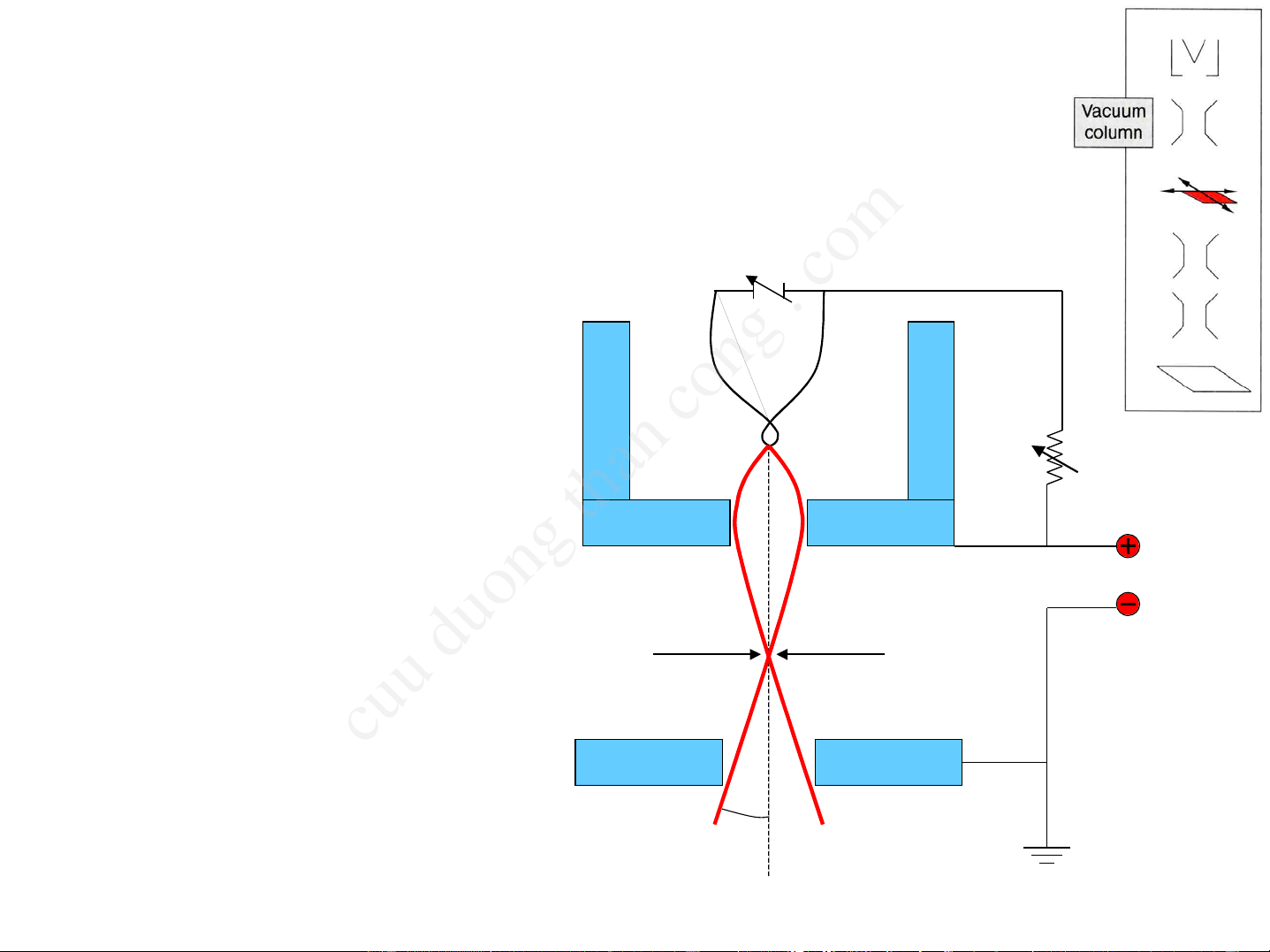
https://fb.com/tailieudientucntt Source: Electron Gun Electrons emitted from filament by thermionic emission (W or LaB6) or from tip by field emission Heater (W single crystal). Filament Wehnelt Accelerated through Cap potential difference V: Bias nearly monochromatic beam of fast electrons. Focused by grounded do Wehnelt Cap. cuu duong than cong . com Anode αo CuuDuongThanCong.com
https://fb.com/tailieudientucntt Thermionic Emission source • Heat a metal substantially (2700K). • Electrons are excited and drawn toward the Anode. • Many electrons transfer through cuu duong than cong . com a hole in the anode and down the beam path. CuuDuongThanCong.com
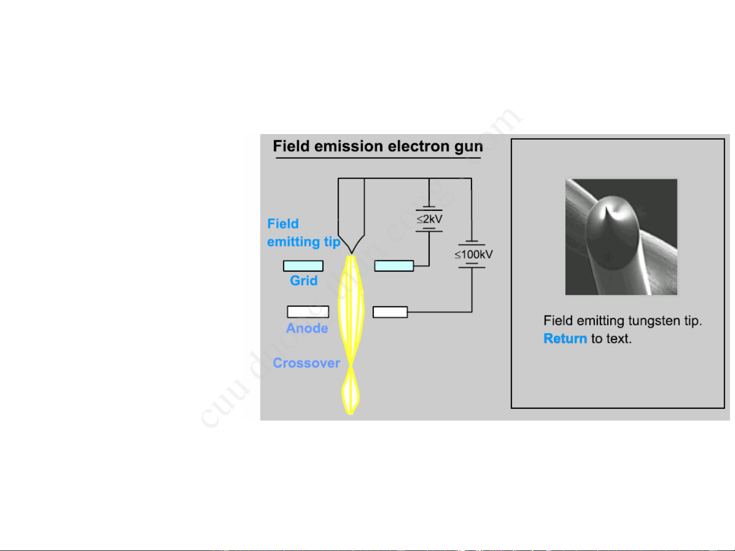
https://fb.com/tailieudientucntt (Cold) Field Emission source • Similar basic design, but now electrons tunnel out of a sharp tip due to strong electric fields. • Smaller emitting area so higher resolution is possible. cuu duong than cong . com CuuDuongThanCong.com
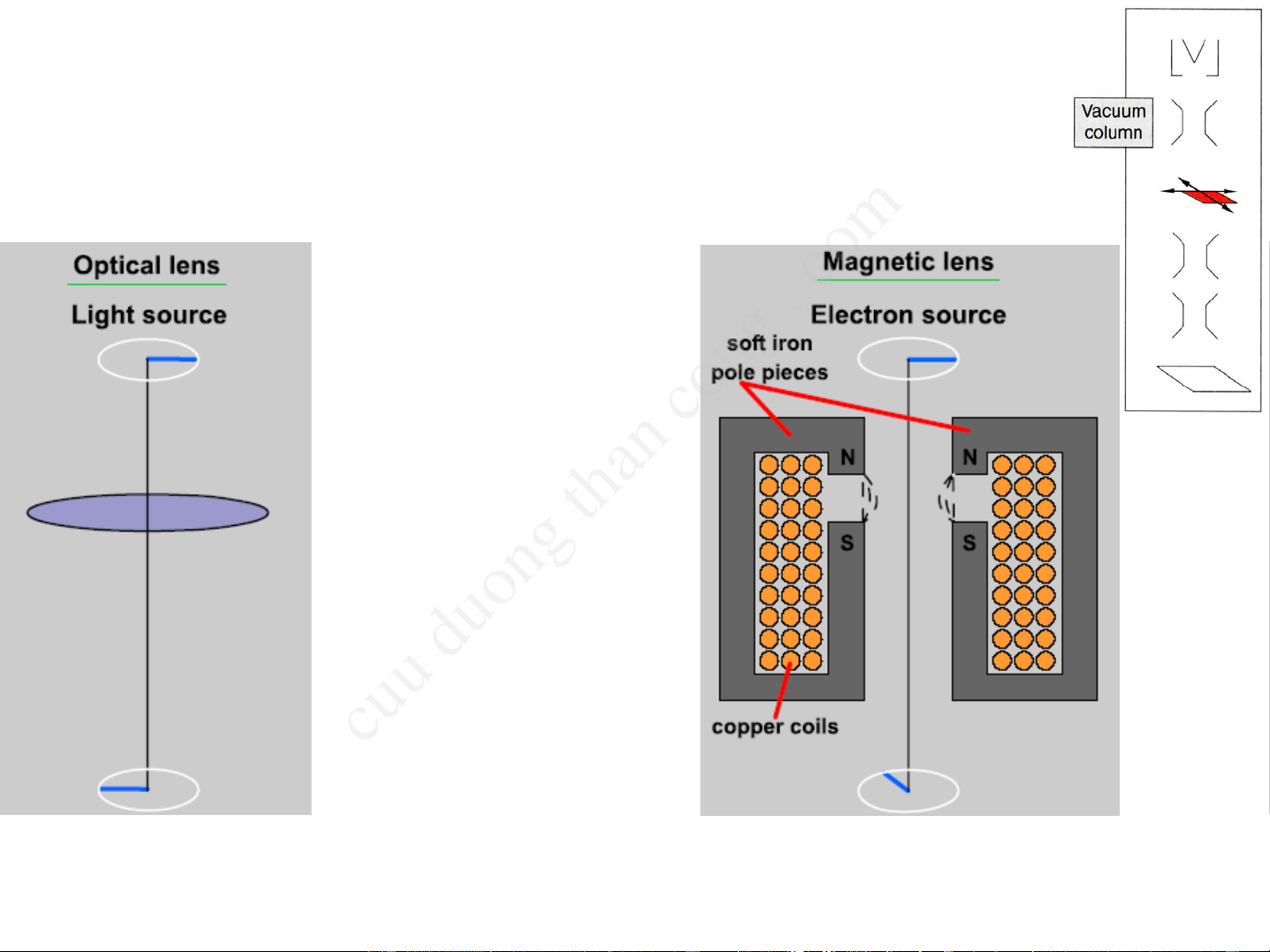
https://fb.com/tailieudientucntt Condensor Lenses EM lenses focus light to as small of a spot as possible, equivalent to convex lenses in optics. cuu duong than cong . com CuuDuongThanCong.com
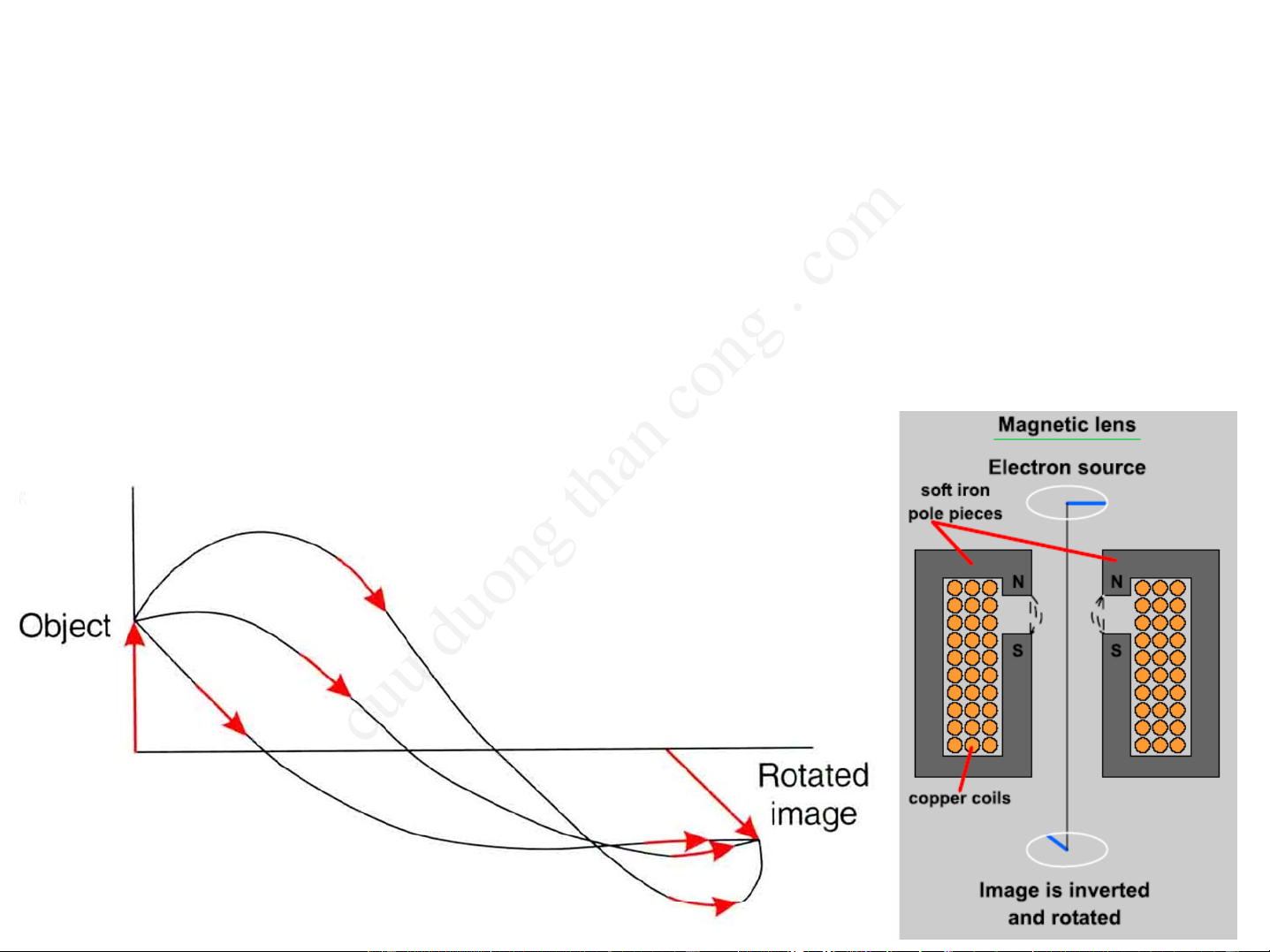
https://fb.com/tailieudientucntt Electron Lenses
• Use electrostatic or electromagnetic fields to focus beams of charged electrons.
• Electromagnetic - Most lenses of this type. Cu wire
coils around soft Fe cores. Sometimes use Fe pole-
pieces to “shape” the field.
– Diagram in book is not too descriptive
• Electrostatic - Unusual, only common example is
the Wehnelt aperture in the electron gun. cuu duong than cong . com CuuDuongThanCong.com
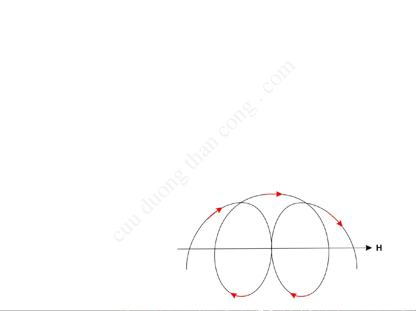
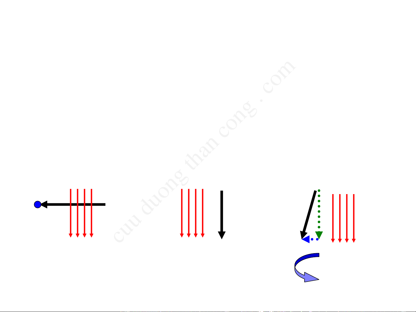
https://fb.com/tailieudientucntt Electrons in magnetic fields
• An electron moving through a perpendicular magnetic field
experiences a [different] perpendicular force – “right hand rule”
• An electron moving parallel to a magnetic field is unaffected.
• An electron moving nearly parallel is slightly deflected out of the
plane, then to the right, then into the plane, then to the left, etc.
– Takes helical path around the magnetic field direction (microscope axis). unaffected electron nearly aligned Force on Magnetic electron electron is field out of plane cuu duong than cong . com No Force Electron follows helical path CuuDuongThanCong.com
https://fb.com/tailieudientucntt
Trajectories in Electromagnetic Lenses
• When adjusting magnification (and focal length), the lens
strength is modified by adjusting the current in the
electromagnetic lens windings.
• Since the magnetic field therefore changes, so do the helical trajectories.
• Ultimately, this leads to image rotation, which needs to be
corrected for, or at least calibrated. cuu duong than cong . com CuuDuongThanCong.com
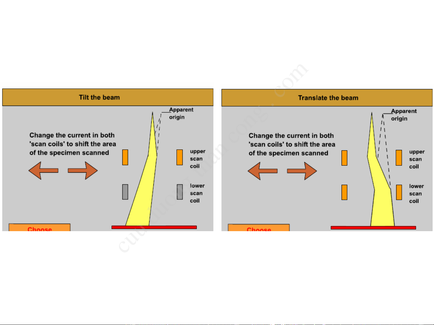
https://fb.com/tailieudientucntt Beam steering
• The electron beam can be positioned for fine
measurements (spot modes) or scanning (SEM, STEM) cuu duong than cong . com CuuDuongThanCong.com
https://fb.com/tailieudientucntt Sample stage • Lateral and normal control • Rotation • Tilt in two directions • Also, possibly integrated: – Heaters – Mechanical testing – Electrical testing cuu duong than cong . com CuuDuongThanCong.com
https://fb.com/tailieudientucntt Objective lens • Electromagnetic. • Usually only ~50x. cuu duong than cong . com CuuDuongThanCong.com
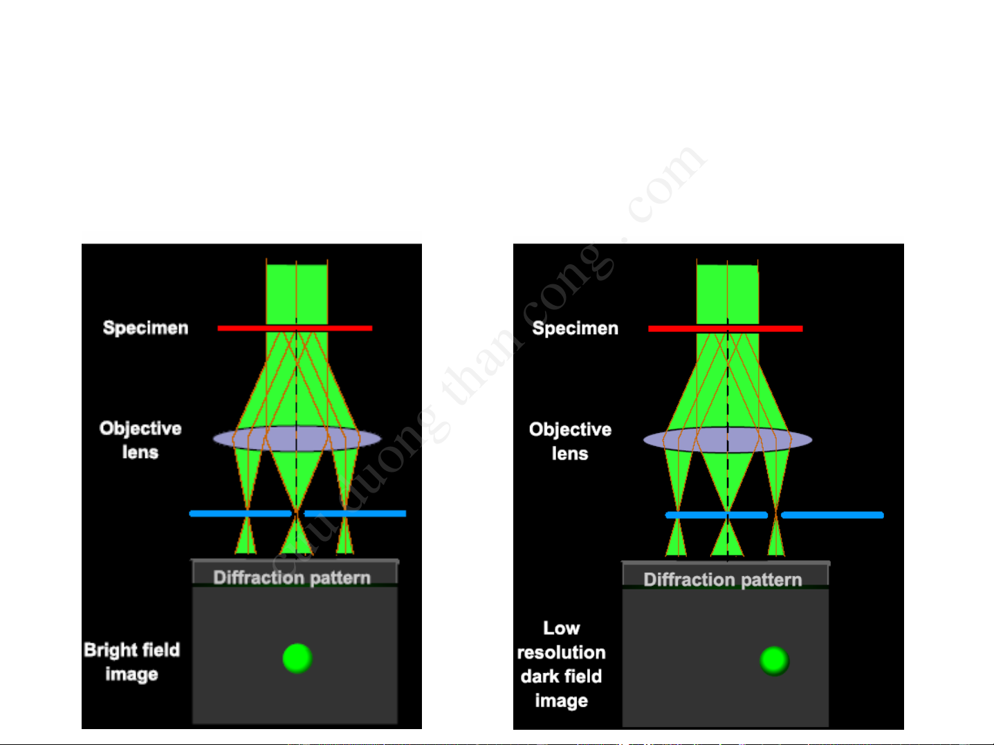
https://fb.com/tailieudientucntt Objective Aperture
• Depending on the aperture position, the bright
field image or the dark field (scattered) image can be collected. cuu duong than cong . com CuuDuongThanCong.com
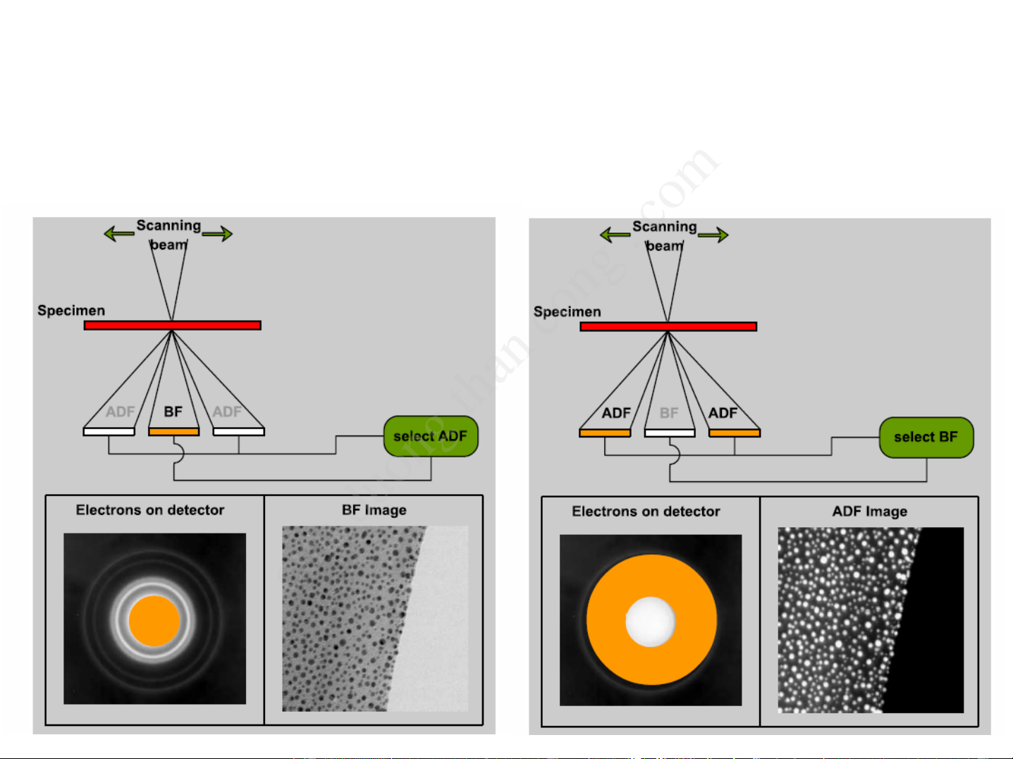
https://fb.com/tailieudientucntt STEM (scanning TEM)
• By selecting bright or dark field electrons, contrast
varies and provides information about crystallography. cuu duong than cong . com CuuDuongThanCong.com
https://fb.com/tailieudientucntt
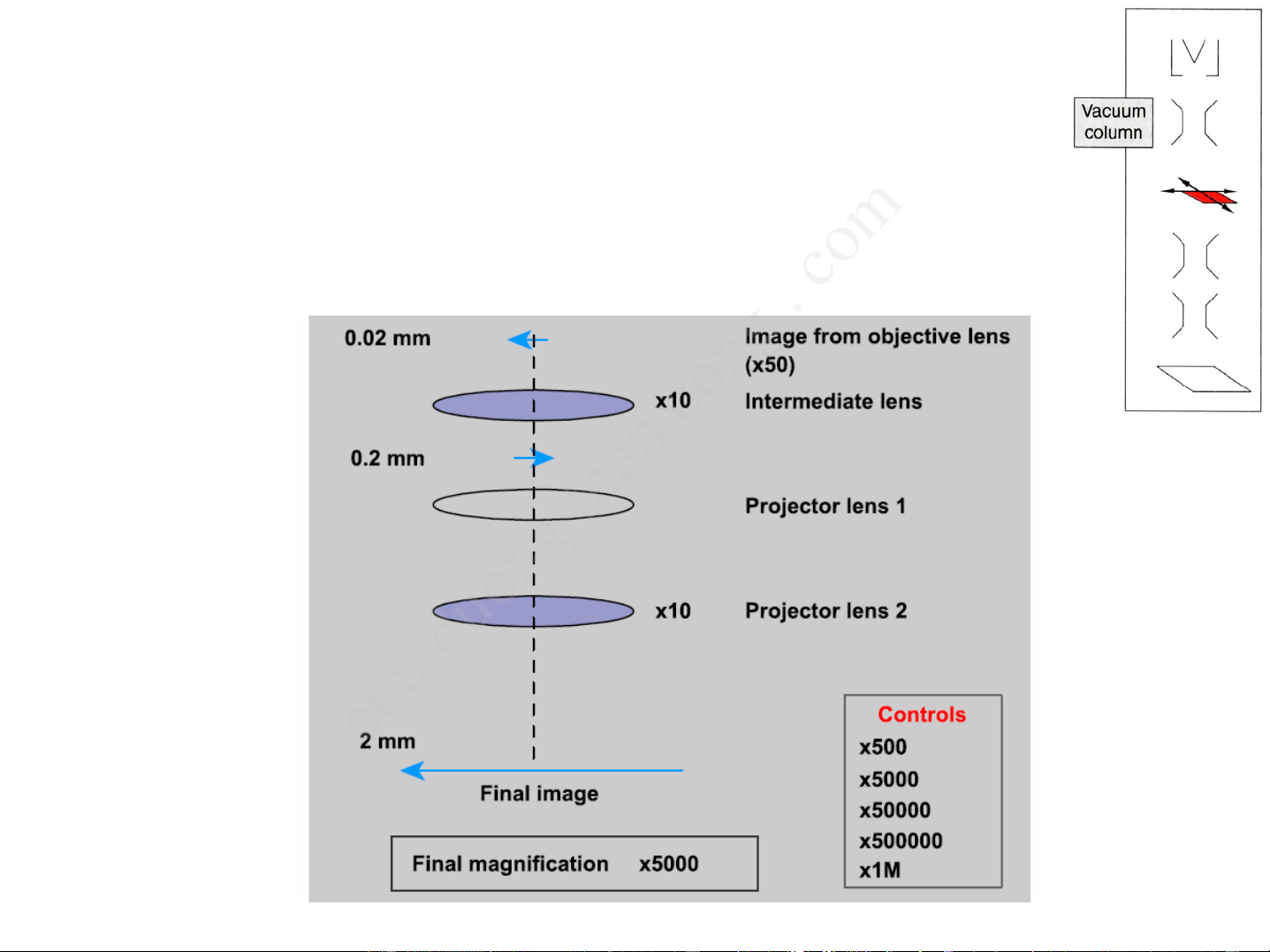
Imaging System (magnification lenses) • Electromagnetic.
• Various combinations employed for increasing magnification. cuu duong than cong . com CuuDuongThanCong.com
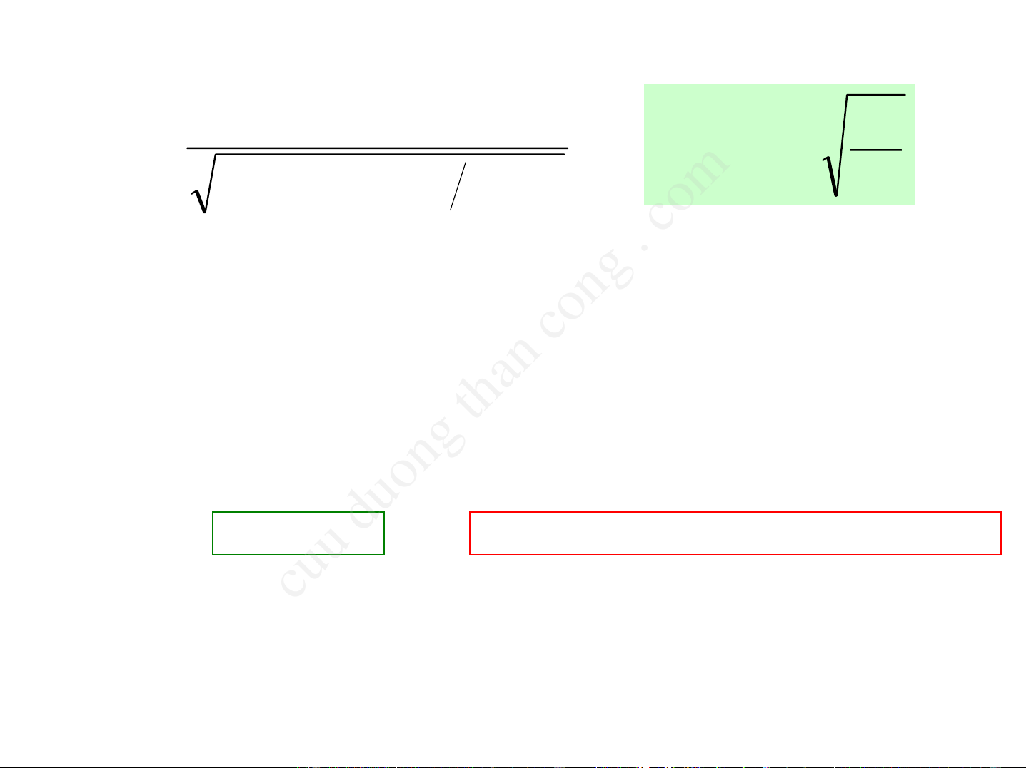
https://fb.com/tailieudientucntt Electron Wavelengths h λ = . 1 5 or λ = nm 2m eV 1 + eV m c V 0 ( 2 0 ) Where: • h - Planck’s constant • m0 - electron rest mass • e - charge on the electron
• V - accelerating voltage (in Volts) • c - speed of light SEM TEM V (kV) 5 20 100 200 300 1000 cuu duong than cong . com λ (nm) .017 .008
0.00370 0.00251 0.00197 0.00087 CuuDuongThanCong.com
https://fb.com/tailieudientucntt Resolution
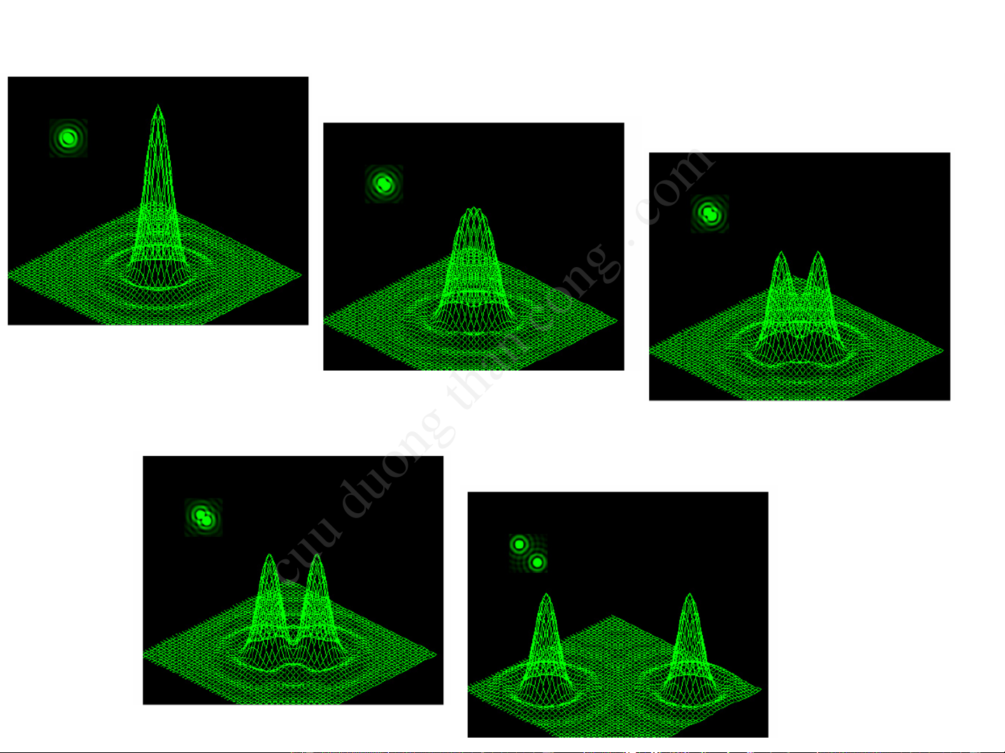
• As features on the surface separate, they may be resolved. cuu duong than cong . com CuuDuongThanCong.com
https://fb.com/tailieudientucntt Resolution
Diffraction Limited - Defined by Raleigh criterion:
δ = 0.61λ /µ sin α ≈ 0.61λ /α d
Since λ varies with V, higher voltages give smaller δ (good) d
but at increased cost and beam damage (bummer).
Also, δ increases as α gets smaller. d
Aberration Limited – The wavelength is so small that
aberrations become extremely important, particularly spherical aberration. δ α3 ≈ s Cs cuu duong than cong . com
Where: Cs - Spherical aberration coefficient
Smaller α gives smaller δ (good), but also lower s intensity (bummer). CuuDuongThanCong.com
https://fb.com/tailieudientucntt
