Experiment 1 Measurement of Resistance, Capacitance, Inductance and Resonant Frequencies of RLC using Oscilloscope môn Vật lý đại cương 2 | Học viện Công Nghệ Bưu Chính Viễn Thông
Purpose: This experiment helps the student understanding a typicalcircuit and the manner to use the equipments including oscilloscope and function generator in electronic engineering. Tài liệu giúp bạn tham khảo, ôn tập và đạt kết quả cao. Mời đọc đón xem!
Môn: Vật lý đại cương 2 298 tài liệu
Trường: Học viện Công Nghệ Bưu Chính Viễn Thông 1.7 K tài liệu
Tác giả:


Preview text:
Experiment 1
Measurement of Resistance, Capacitance, Inductance
and Resonant Frequencies of RLC using Oscilloscope Equipments
1. Dual trace oscilloscope 20 MHz – OS 5020C;
4. Electrical board and wires;
2. Function generator GF 8020H;
5. Devices including resistor, 3. Changeable resistance box; capacitor, and coil;
Purpose: This experiment helps the student understanding a typical circuit and the
manner to use the equipments including oscilloscope and function generator in
electronic engineering, namely measuring the physical parameters of the resistor,
capacitor, and inductor as well as the resonant frequency of RLC circuit. I. THEORETICAL BACKGROUND 1. RLC circuit
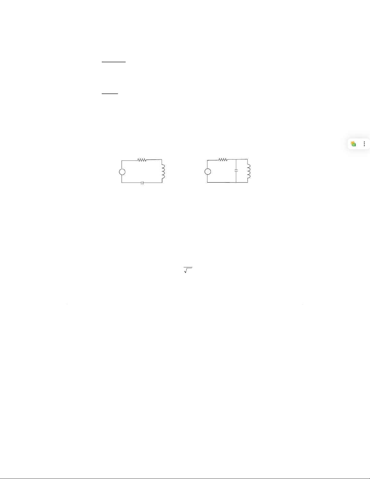
An RLC circuit (also known as a resonant circuit or a tuned circuit) is a typical one
consisting of a resistor (R), an inductor (L), and a capacitor (C), connected in series or in parallel (figure 1). R R ∼ ∼ L E E C L C
Figure 1. Series (left) and parallel (right) RLC circuit
RLC circuits have many applications particularly for oscillating circuits and in radio and
communication engineering. Every RLC circuit consists of two components: a power
source and resonator. Likewise, there are two types of resonators – series LC and parallel
LC. The expressions for the bandwidth in the series and parallel configuration are
inverses of each other. This is particularly useful for determining whether a series or
parallel configuration is to be used for a particular circuit design. However, in circuit
analysis, usually the reciprocal of the latter two variables is used to characterize the
system instead. They are known as the resonant frequency and the damping factor (or the Q factor) respectively.
The undamped resonance or natural frequency of an LC circuit (in radians per second) is given by: 0= ω 1 (1) lC
In the more familiar unit hertz (or inverse seconds), the natural frequency becomes, ω0 1 = f0= (2) π 2 π 2 lC
Resonance occurs in RLC circuit when the complex impedance ZLC of the LC resonator becomes zero, ZLC = ZL + ZC = 0 (3)
Then ω0 becomes exactly the resonant frequency of RLC circuit.
The damping factor of the circuit (in radians per second) for a series RLC circuit is, R β = (4) L 2
and for a parallel RLC circuit: 1 β = (5) RC 2
For applications in oscillator circuits, it is generally desirable to make the damping factor
as small as possible, or equivalently, to increase the quality factor (Q) as much as
possible. In practice, this requires decreasing the resistance R in the circuit to as small as
physically possible for a series circuit, and increasing R to as large a value as possible for
a parallel circuit. In this case, the RLC circuit becomes a good approximation to an ideal LC circuit.
In this experiment, the RLC circuit will be investigated by an oscilloscope. Using this
equipment we can determine the resistance of a resistor, capacity of a capacitor, and
inductivity of a coil as well as the resonant frequency of a series and a parallel RLC circuit.
2. Introduction to oscilloscope 2.1. General description
An oscilloscope (abbreviated as OS) is a electronic test equipment that allows signal
voltages to be viewed, usually as a two-dimensional graph of one or more electrical
potential differences (horizontal axis) plotted as a function of time or of some other voltage (vertical axis).
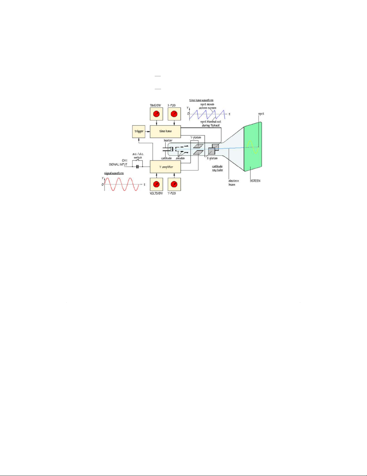
The simplest type of OS consists of a cathode ray tube (CRT), a vertical amplifier, a
time-base, a horizontal amplifier and a power supply as shown in figure 2.
CRT is a highly evacuated glass envelope (10-6 mmHg) with its flat face covered in a
fluorescent material (phosphor). In the neck of the tube is an electron gun, which is a
heated metal plate (FF) with a wire mesh (the grid G) in front of it. A small grid potential
is used to block electrons from being accelerated when the electron beam needs to be
turned off, as during sweep retrace or when no trigger events occur. A potential
difference of about 1000 V is applied to make the heated plate (the cathode) negatively
charged relative to the anodes A1 and A2. It increases the energy (speed) of the electrons
that strike the fluorescent screen later. However, before striking the screen, the electron
beam goes through two opposed pairs of metal plates called the deflection plates. The
vertical amplifier generates a potential difference (Uy) across one pair of plates (Y1Y2),
giving rise to a vertical electric field through which the electron beam passes. In general,
the amplifier has a very high input impedance, typically one MΩ, so that it draws only a
tiny current from the signal source. When the top plate is positive with respect to the
bottom plate, the beam is deflected upwards; when the field is reversed, the beam is
deflected downwards. The horizontal amplifier does a similar job with the other pair of
deflection plates (X1X2), causing the beam to move left or right by potential difference
Ux. The instantaneous position of the beam will depend upon the Ux and Uy voltages.
Let x as the horizontal deflection when Ux is applied to plates X1X2, and y the vertical
one when Uy is applied to plates Y1Y2. By definition we have: x α =
is the horizontal sensitivity of CRT (6) xU x y α =
is the vertical sensitivity of CRT yU y Y1 X1 F G A1 A2 F X2 Y2
Figure 2. Structure of an oscilloscope
When hitting the screen, the kinetic energy of the electrons is converted by the phosphor
into visible light at the point of impact. In general, when switched on, a CRT normally
displays a single bright dot in the center of the screen.
Assuming that the input signal Uy is applied to the plates Y1Y2 (Y-channel): Uy = U0y.cos ωt (7)
As a result, the bright dot in the screen will oscillate. Due to the image keeping of retina,
a vertical light line can be observed on the screen. The length of this light line is
proportional to amplitude U0y: y = Kα.2U0y = Ky.2U0y (8)
where K is amplification factor of Y-amplifier and Ky = K α is the vertical sensitivity or Y-channel transmittance.
Similarly, when Ux is applied to the plates X1X2 (X-channel): Ux = U0x.cos ωt (9)
Then a horizontal light line can be observed on the screen with the length: x = Kα.2U0x = Kx.2U0x (11)
where Kx is the horizontal sensitivity or X-channel transmittance.
If an alternative voltage in the form of Uy is applied to plates Y1Y2 and a voltage that
changes continuously and linearly with time Ux = a.t applied to plates X1X2
simultaneously, the bright line on the screen will represent the total motion of two
oscillations which are perpendicular with each other. x = Kx.Ux = kx.at ωx = = 0 = (12) y K . 0 . .cosω . .cos y U y K y U y t K y U y K xa
The electron beam draw on screen a signal y = y(x) similarly to the investigated one.
The time-base component is an electronic circuit that generates a ramp voltage or saw-
tooth waveform. This is a voltage that changes continuously and linearly with time, Ux = a.t (13)
until the maximum value Umax then decreases gradually to the initial voltage U0.
When Ux is applied to X plates it sweeps the electron beam at constant speed from left to
right across the screen and then quickly returns the beam to the left in time to begin the
next sweep. The time-base can be adjusted to match the sweep time to the period of the
signal TS and sweep frequency f. f1= (14) Ts
Let T is the period of the input signal then:
• If Ts = T: a total oscillation can be observed on the screen.
• If Ts = nT (n is integer): n total oscillations can be observed on the screen.
• If Ts ≠ nT: a complicated oscillation or oscillation in motion can be observed on the screen.
There is a knob on the front panel of the Oscilloscope
oscilloscope for adjusting the sweep frequency.
This knob allows keeping the value of U0 and Umax
constant and changing the sweep speed,
consequently the sweep frequency and the slope of
graph Ux(t). By adjusting this knob so that Ts = nT
n stable total oscillations can be observed on the screen. Y-channel input
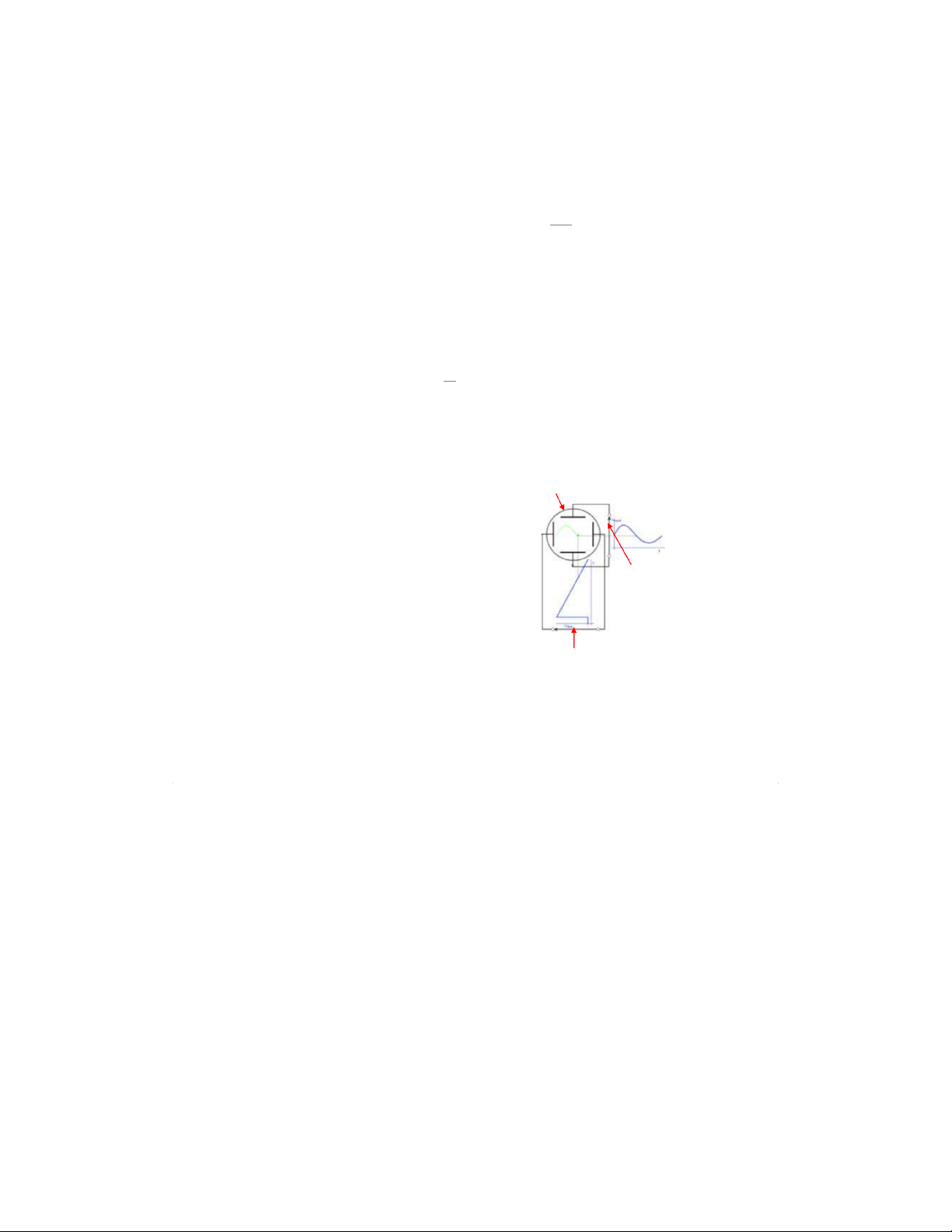
2.2. Symbol of oscilloscope in electric circuit
OS is symbolized in the diagram of a electric
circuit by two pairs of parallel lines inside a
circular (figure 3) characterizing two pairs of the X-channel input
deflection electrodes. In this case, X-channel
Figure 3. Symbol of oscilloscope
consists of horizontal pair of which the left is in electric circuit
symbolized as the positive plate and the right as the
negative one (connected to the ground). Y-channel consists of vertical pair of which the
upper is symbolized as the positive plate and the lower as the negative one (connected to the ground).
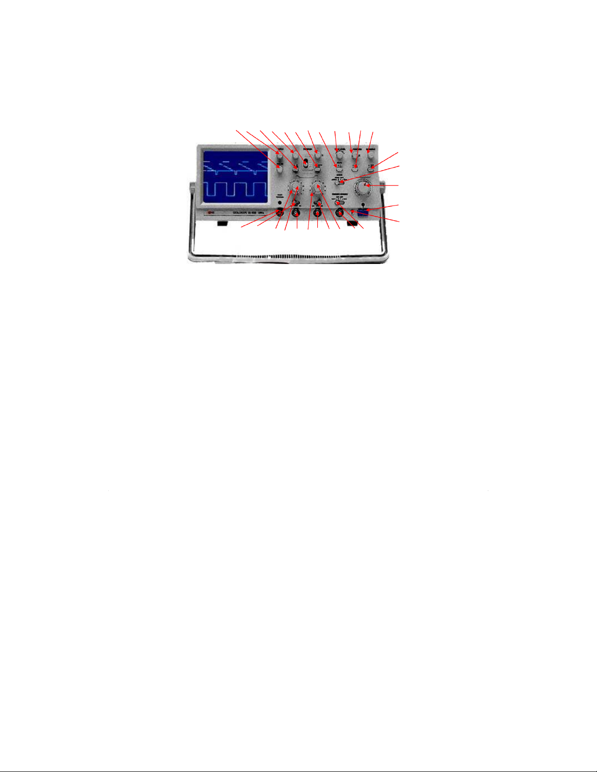
A typical OS is usually box shaped with a display screen, numerous input connectors,
control knobs and buttons on the front panel. To aid measurement, a grid called the
graticule is drawn on the face of the screen. Each square in the gratitude is known as a
division. In this experiment, a dual trace oscilloscope OS 5020 C is used for
measurements. It is illustrated in figure 4. 1 2 3 54 6 8 7 9 10 11 12 13 14 15 16 17
28 27 26 25 24 23 22 21 20 19 18
Figure 4. Front panel of oscilloscope OS 5020C
1. Adjustor of electron beam convergence
15. Individual/dual adjustor for signal time
2. Adjustor of light intensity 16. On/off power switch
3. Switch of X-channel scale (X1 or X10) 17. Polarity inversion switch
4. Adjustor for moving electron beam up 18. and down 19.
5. Switch of channel and measurement
20. Amplitude adjustor for Y-channel option 21. DC/AC/GROUND switch for Y-
6. Switch of Y-channel scale (X1 or X10) channel
7. Adjustor for moving electron beam 22. Y-channel input vertically
23. Adjustor for sensitivity in range of 8. Signal slope switch
X5mV/div. to X20V/div. for Y-channel
9. Adjustor for signal balance 24. X-channel input
10. Adjustor for moving electron beam
25. Amplitude adjustor for X-channel horizontally
26. Adjustor for sensitivity in range of
11. Switch of sweep magnification (X10)
X5mV/div. to X20V/div. for X-channel
12. Adjustor of calibrated signal time 27. DC/AC/GROUND switch for X-
13. On/off standard regime switch channel 14. 28. Ground
2.3. Resultant signal form produced by two perpendicular oscillations
If an alternative voltage Uy = U0y.cos( ωy.t+ϕ ) is applied to plates Y1Y2 and other voltage
Ux = U0x.cos(ωxt+ϕ) applied to plates X1X2 simultaneously, the bright line on the screen
will represent the total motion of two oscillations which are perpendicular with each other. x = Kx.Ux = x0.cosωxt (15)
y = Ky.Uy = y0.cos(ωy.t+ϕ ) (16)
When ωx = ωy (in case of n = 1), the electron beam will produce an trace on the screen
defined by the following equation: 2 2 ⎛ ⎞ ⎛ ⎞ x − + y 2 =xy ϕ (17) 2 cos sin ϕ ⎜ ⎜ ⎟ ⎟ ⎜ ⎜ ⎟ ⎟ ⎝x0 ⎠ ⎝ 0 y ⎠ 0 x y0
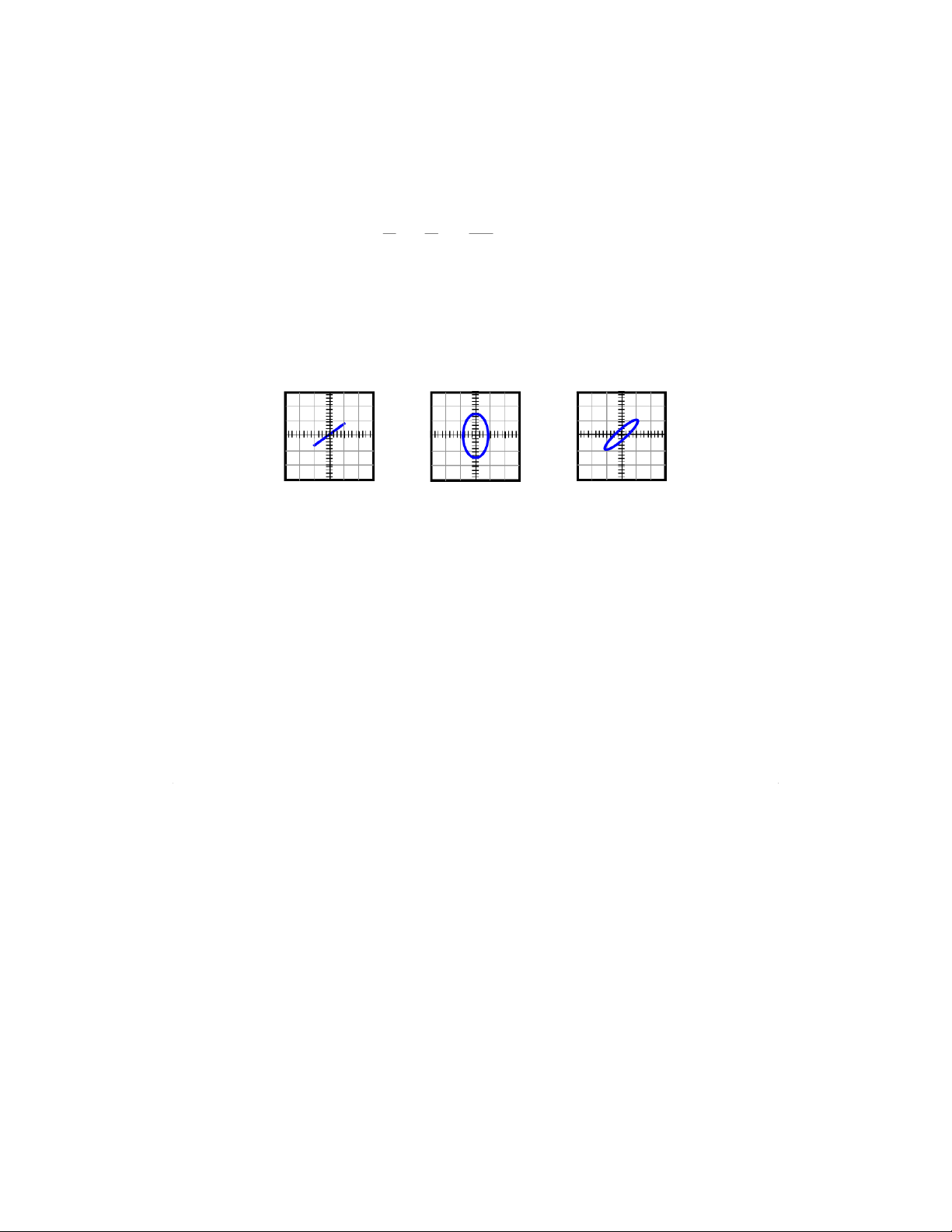
The trace may be either a line or oval depending on the value of the oscillation phase:
• If ϕ = 0 and ϕ = π, a diagonal line (figure 5a) is displayed. It is corresponding to resistance circuit.
• If ϕ = ± π/2, a vertical oval trace is displayed (figure 5b). It is corresponding to
either RC or LR circuit. If a suitable resistor is used so that U0x = U0y a circular trace will be displayed.
• If ϕ gets an arbitrary value then the trace will be an oblique oval (figure 5c). It is
corresponding to RLC circuit. In case of resonance that is the case of ZL = ZC as
mentioned above in part 1, a diagonal line is displayed as shown in figure 5a. (a) (b) (c)
Figure 5. Signal form on oscilloscope screen produced by two perpendicular oscillations
3. Introduction to function generator
A function generator (FG) is a device containing an electronic oscillator, a circuit that is
capable of creating a repetitive waveform. The most common waveform is a sine wave,
but saw-tooth, step (pulse), square, and triangular waveform. Function generators are
typically used in simple electronics repair and design; where they are used to stimulate a
circuit under test. The oscilloscope is then used to measure the circuit's output. Function
generators vary in the number of outputs they feature, frequency range, frequency
accuracy and stability, and several other parameters.
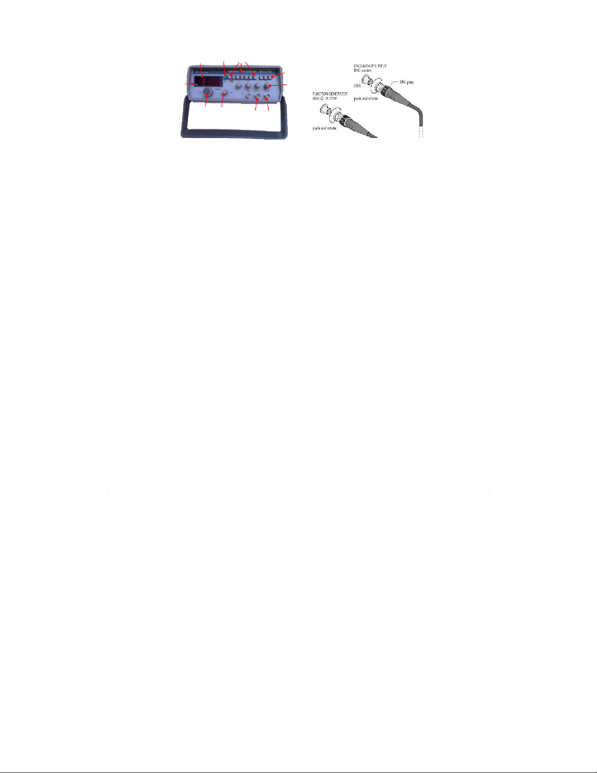
The function generator GF8020F used in this experiment is shown in figure 6a. A typical
FG can provide frequencies up to 20 MHz and uses a BNC connector, usually requiring a
50 or 75 ohm termination as shown in figure 6b. This connector is also used for OS in measurement. 1 10 3 4 2 5 8 9 7 6 (a) (b)
Figure 6. Front panel of function generator GF8020F (a) and BNC connector (b)
(1. On/off power switch; 2. LED indicating power on; 3. Scale switching buttons of
generated frequency range, e.g 1K, 10K, and 100K (Hz); 4. switching button for output
option of sine waveform; 5. Adjustor for output voltage amplitude; 6. Voltage output for
BNC connection; 7. Voltage output of square pulse; 8. Adjustor for rough frequency;
9. Adjustor for fine frequency; 10. LEDs display of output frequency) II. EXPERMENTAL PROCEDURE A. Preparation
1.1 Learn to know the way of using oscilloscope.
1.2 Learn to know the way of using function generator.
1.3. Learn to know the way of using BNC connection and measurement probs.
B. Measurement of resistance, capacitance, and inductance
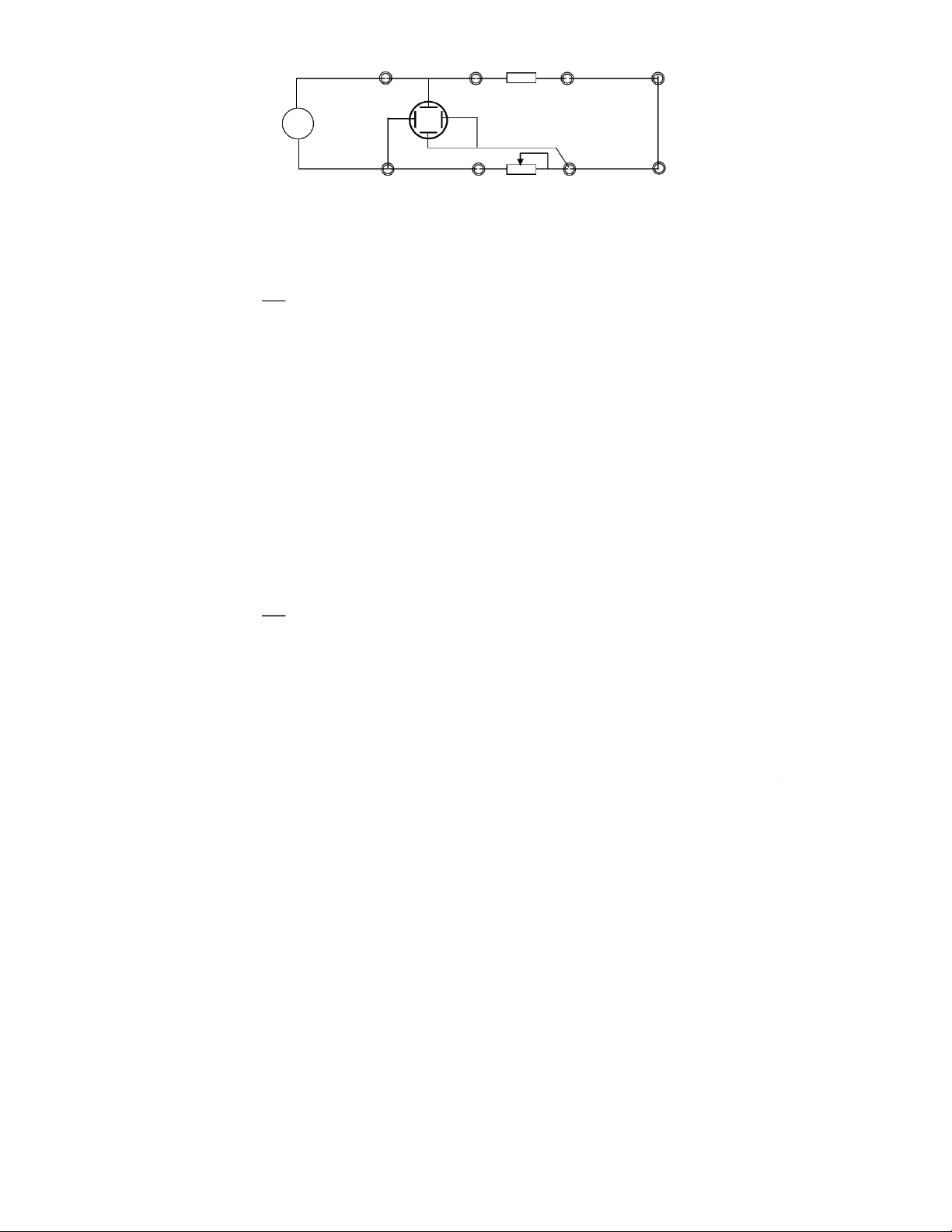
1. Resistance measurement of unknown resistor
1.1. Connect all the terminals using the banana plug cords and install resistance box
(denoted as R0) and unknown resistor RX based on the circuit layout shown in figure 7.
1.2. Switch to power on FG. Choose the frequency range of 1K (using button group 3)
and sine waveform (using button 4). Adjust knobs 8 and 9 to set an initial measurement
frequency of about 500 Hz (or 1000 Hz).
1.3. Switch to power on OS. Observe to see a trace in the form of a illuminated vertical line displayed on the screen. A R A X Y FG OS 8020H X 5020C B R B C C 0
Figure 7. Circuit layout for measurement of resistance, capacity, and inductivity
1.4. Regulating the resistance box R0 so that the trace displayed on screen of OS becomes
a diagonal line. Then, UX = UY = URo that is, RX = R0 (18)
Make a data table (denoted table 1) then record the value of frequency f and the respective value of R0 in it.
Note: the resistance box R0 are regulated by turning up its knobs with the order from
greater range (∼thousands ohm) to smaller one (∼ohm or ∼one tenths ohm), respectively.
1.5. Repeat the experimental procedure with other frequencies (may be either 1000, and
1500 Hz or 1500, and 2000 Hz).
1.6. Turn off OS and FG; turn down the knobs of the changeable resistor R0 to zero
positions and uninstall the resistor RX from the measurement circuit in order to prepare for next measurement.
2. Capacitance measurement of unknown capacitor
2.1. Install the unknown capacitor CX at the position of the measured resistor RX as shown in figure 7.
2.2. Switch to power on FG. Choose the frequency range of 10K (using button group 3)
and sine waveform (using button 4). Adjust knobs 8 and 9 to set an initial measurement frequency of about 1000 Hz.
2.3. Switch to power on OS. Observe to see a trace in the form of illuminated upright
oval displayed on the screen. For convenient and exact observing, adjust knobs 7 and 10
to move the oval trace so that its center is coincided with the center of the coordinate axes of the screen.
2.4. Regulating the resistance box R0 so that the oval trace becomes a circle.
Make a data table (denoted table 2) then record the value of frequency f and the respective value of R0 in it.
Note: Regulating the resistance box R0 by turning up its knobs with the order from
greater range (∼thousands ohm) to smaller one (∼ohm or ∼one tenths ohm), respectively.
2.5. Complete the table 2 by performing this manipulation for more 2 times according to
2 different frequencies (may be either 1500, and 2000 Hz or 2000, and 3000 Hz).
2.6. Turn off OS and FG; turn down the knobs of resistance box R0 to zero positions, and
uninstall the capacitor CX from the board in order to prepare for next measurement.
3. Inductance measurement of unknown coil
3.1. Install the unknown coil LX at the position of the measured resistor RX as shown in figure 7.
3.2. Switch to power on FG. Choose the frequency range of 10K (using button group 3)
and sine waveform (using button 4). Adjust knobs 8 and 9 to set an initial measurement frequency of about 10.000 Hz.
3.3. Switch to power on OS. Observe to see a trace in the form of illuminated upright
oval displayed on the screen. For convenient and exact observing, adjust knobs 7 and 10
to move the oval trace so that its center is coincided with the center of the coordinate axes of the screen
3.4. Regulating the resistance box R0 so that the oval trace becomes a circle.
Make a data table (denoted table 3) then record the value of frequency f and the respective value of R0 in it.
Note: Regulating the resistance box R0 by turning up its knobs with the order from
greater range (∼thousands ohm) to smaller one (∼ohm or ∼one tenths ohm), respectively.
3.5. Complete the table 3 by performing this manipulation for more 2 times according to
2 different frequencies (may be either 15.000, and 20.000 Hz or 20.000, and 30.000 Hz).
3.6. Turn off OS and FG; turn down the knobs of the resistance box R0 to zero positions,
at last, uninstall the coil LX from the board in order to prepare for next measurement.
C. Determination of resonant frequency of RLC circuit 1. Series RLC circuit
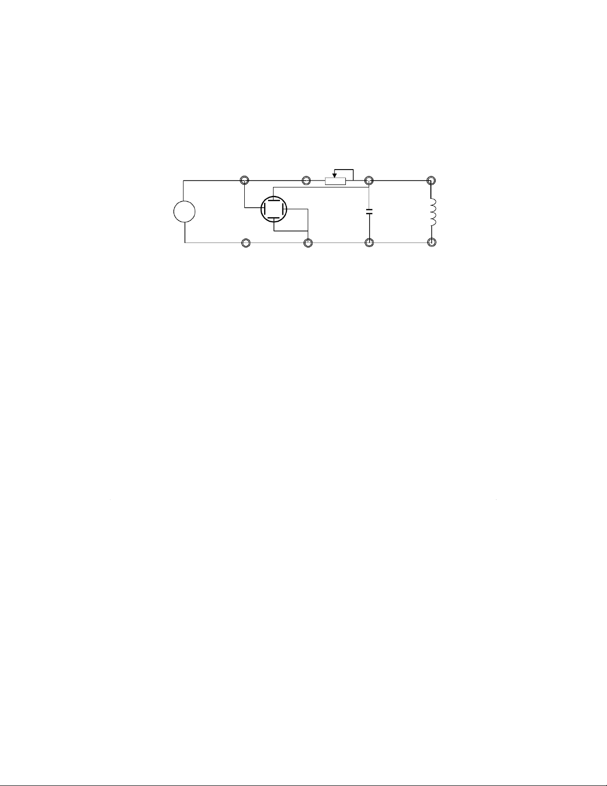
1.1. Connect all the terminals using the banana plug cords, and install the resistance box
R0, the measured capacitor CX, and coil LX based on the circuit layout shown in figure 8.
Set a value of 1000 Ohm for R0. A A R 0 Y FG X OS LX 8020H 5020C B B CX
Figure 8. Series RLC circuit layout for measurement of resonant frequency
1.2. Switch to power on FG. Choose the frequency range of 100K (using button group 3)
and sine waveform (using button 4).
1.3. Switch to power on OS. Observe to see to see an inclined oval trace displayed on the screen of OS.
1.4. Regulating the knobs 8 and 9 of FG to change the generated frequency so that. The
oval trace becomes an inclined line.
Make a data table (denoted table 4) then record the values of resonant frequency fserries in it.
1.5. Repeat the experimental procedure for more 2 times.
1.6. Turn off OS and FG and uninstall the capacitor CX from the measurement circuit in
order to prepare for next measurement. 2. Parallel RLC circuit
2.1. 1.1. Connect all the terminals using the banana plug cords, and install the resistance
box R0, the measured capacitor CX, and coil LX based on the circuit layout shown in
figure 9. Set a value of 1000 Ohm for R0. A A R 0 Y X FG OS LX 8020H 5020C CX B B
Figure 9. Parallel RLC circuit layout for measurement of resonant frequency
2.2. Switch to power on FG. Choose the operational regimes similarly part 1.
2.3. Switch to power on OS. Observe to see if an oblique ellipsoid occurs on the screen.
1.3. Switch to power on OS. Observe to see to see an inclined oval trace displayed on the screen of OS.
1.4. Regulating the knobs 8 and 9 of FG to change the generated frequency so that. The
oval trace becomes an inclined line.
Insert an additional column in table 4 then record the values of resonant frequency fparallel in it.
2.5. Repeat the experimental procedure for more 2 times.
2.6. Turn off OS and FG and uninstall the resistance box R0, capacitor CX and coil LX
from the measurement circuit. At last, put all the devices in order. 3. REQUIREMENTS
3.1. Before doing the experiment
Read carefully the instruction to understand:
- the structure and operational principle of oscilloscope, the way to connect OS with a
circuit and to manage the signal trace displayed on the oscilloscope’s screen.
- the way to connect FGs with a circuit and to change the signal forms as well as their frequencies.
3.2. After doing the experiment
Complete the experimental report with the following requirements:
- Calculate the unknown resistance.
- Calculate the unknown capacitance
when UC = UX = UY = URo it leads to 1R = Z X= 0 (19) 2π .f .CX 1 Hence: CX = (20) 2π. f.R0
- Calculate the unknown inductance
when, UC = UX = UY = URo it results in, L Z X f L= 2π . R . = (21) 0 R Hence: L 2 0 X. = f (22) π
- Compare the measured value of series and parallel resonant frequency together and. also
with the predicted value using eq. (2) where L and C are the calculated capacitance and
inductance as suggested in eq. (20) and (22).
Tài liệu liên quan:
-
Bài tập Vật lý nguyên tử môn Vật lý đại cương 2 | Học viện Công Nghệ Bưu Chính Viễn Thông
11 6 -
Bài tập Vật lý nguyên tử môn Vật lý đại cương 2 | Học viện Công Nghệ Bưu Chính Viễn Thông
12 6 -

Tán xạ ánh sáng và Hiệu ứng Tyndall - Lý thuyết và Ứng dụng môn Vật lý đại cương 2 | Học viện Công Nghệ Bưu Chính Viễn Thông
19 10 -

Chương 23: Quang học lượng tử môn Vật lý đại cương 2 | Học viện Công Nghệ Bưu Chính Viễn Thông
17 9 -

Chương 24: Cơ Học Lượng Tử - Tính Sóng-Hạt và Phương Trình Schrödinger môn Vật lý đại cương 2 | Học viện Công Nghệ Bưu Chính Viễn Thông
18 9