Instruction Set Overview: Key Registers and Addressing Modes | Môn Electrical Engineering - Trường Đại học Quốc tế, Đại học Quốc gia Thành phố Hồ Chí Minh
Instruction Set Overview: Key Registers and Addressing Modes Môn Electrical Engineering. Tài liệu được sưu tầm gồm 131 trang, giúp bạn ôn tập tốt hơn. Mời các bạn đón xem.
Môn: Electrical Engineering 8 tài liệu
Trường: Trường Đại học Quốc tế, Đại học Quốc gia Thành phố Hồ Chí Minh 2 K tài liệu
Tác giả:


Preview text:
lOMoAR cPSD| 58583460 lOMoAR cPSD| 58583460
Instruction Set Nomenclature Status Register (SREG) SREG: Status Register C: Carry Flag Z: Zero Flag N: Negative Flag 8- bit V:
Two’s complement overflow indicator Instruction Set S: N ⊕ V, For signed tests H: Half Carry Flag T:
Transfer bit used by BLD and BST instructions I:
Global Interrupt Enable/Disable Flag Registers and Operands Rd:
Destination (and source) register in the Register File Rr:
Source register in the Register File R:
Result after instruction is executed K: Constant data k: Constant address b:
Bit in the Register File or I/O Register (3-bit) s:
Bit in the Status Register (3-bit) X,Y,Z: Indirect Address Register
( X=R27:R26, Y=R29:R28 and Z =R31:R30) A: I/O location address q:
Displacement for direct addressing (6-bit) Rev. 0856H–AVR–07/09 lOMoAR cPSD| 58583460 AVR Instruction Set I/O Registers RAMPX, RAMPY, RAMPZ
Registers concatenated with the X-, Y-, and Z-registers enabling indirect addressing of the whole data space on MCUs with
more than 64K bytes data space, and constant data fetch on MCUs with more than 64K bytes program space. RAMPD
Register concatenated with the Z-register enabling direct addressing of the whole data space on MCUs with more than 64K bytes data space. EIND
Register concatenated with the Z-register enabling indirect jump and call to the whole program space on MCUs with more
than 64K words (128K bytes) program space. Stack
STACK: Stack for return address and pushed registers SP: Stack Pointer to STACK Flags ⇔: Flag affected by instruction 0: Flag cleared by instruction 1: Flag set by instruction -:
Flag not affected by instruction
The Program and Data Addressing Modes
The AVR Enhanced RISC microcontrol er supports powerful and efficient addressing modes for access to the Program
memory (Flash) and Data memory (SRAM, Register file, I/O Memory, and Extended I/O Memory). This section describes
the various addressing modes supported by the AVR architecture. In the following figures, OP means the operation code
part of the instruction word. To simplify, not al figures show the exact location of the addressing bits. To generalize, the
abstract terms RAMEND and FLASHEND have been used to represent the highest location in data and program space, respectively. Note:
Not all addressing modes are present in al devices. Refer to the device spesific instruction summary.
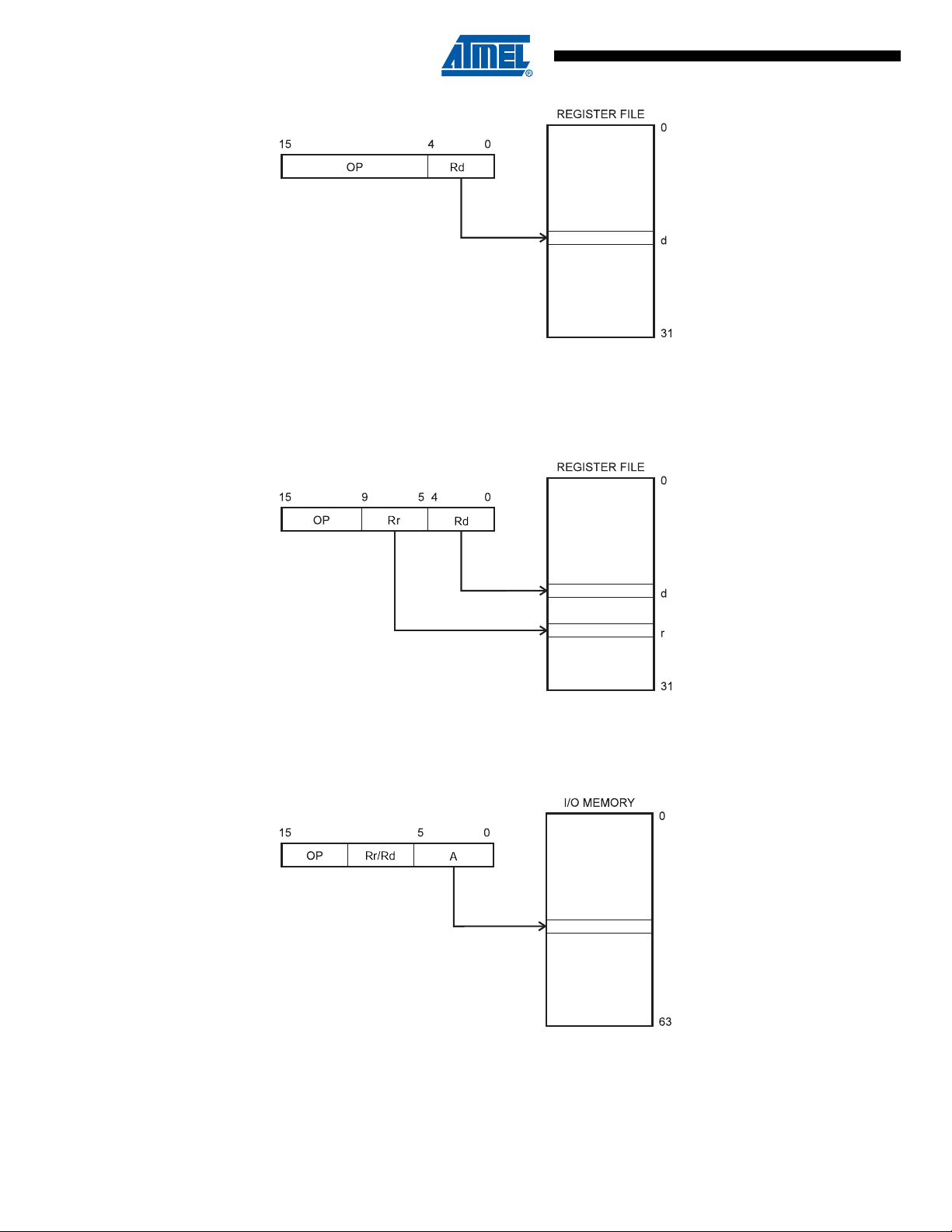
Register Direct, Single Register Rd
Figure 1. Direct Single Register Addressing lOMoAR cPSD| 58583460
The operand is contained in register d (Rd).
Register Direct, Two Registers Rd and Rr
Figure 2. Direct Register Addressing, Two Registers
Operands are contained in register r (Rr) and d (Rd). The result is stored in register d (Rd). I/O Direct
Figure 3. I/O Direct Addressing
Operand address is contained in 6 bits of the instruction word. n is the destination or source register address. lOMoAR cPSD| 58583460 AVR Instruction Set
Note: Some complex AVR Microcontrollers have more peripheral units than can be supported within the 64 locations reserved in the
opcode for I/O direct addressing. The extended I/O memory from address 64 to 255 can only be reached by data addressing, not I/O addressing. Data Direct
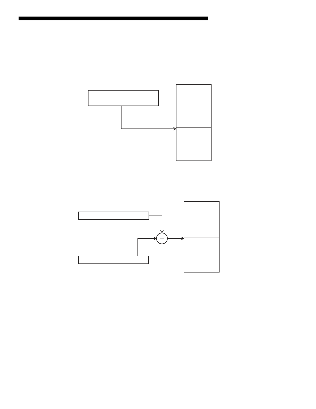
Figure 4. Direct Data Addressing Data Space 31 2019 16 0x0000 OP Rr/Rd Data Address 15 0 RAMEN D
A 16-bit Data Address is contained in the 16 LSBs of a two-word instruction. Rd/Rr specify the destination or source register.
Data Indirect with Displacement
Figure 5. Data Indirect with Displacement Data Space 0x0000 15 0 Y OR Z - REGISTER 15 10 65 0 OP Rr/Rd q RAMEN D
Operand address is the result of the Y- or Z-register contents added to the address contained in 6 bits of the instruction
word. Rd/Rr specify the destination or source register. Data Indirect
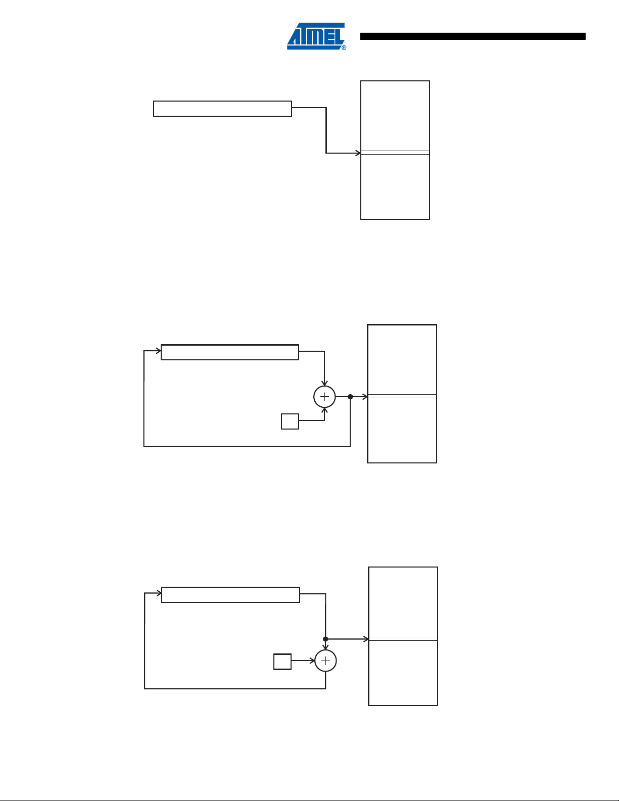
Figure 6. Data Indirect Addressing lOMoAR cPSD| 58583460 Data Space 0x0000 15 0 X, Y OR Z - REGISTER RAMEND
Operand address is the contents of the X-, Y-, or the Z-register. In AVR devices without SRAM, Data Indirect Addressing is
called Register Indirect Addressing. Register Indirect Addressing is a subset of Data Indirect Addressing since the data
space form 0 to 31 is the Register File.
Data Indirect with Pre-decrement
Figure 7. Data Indirect Addressing with Pre-decrement Data Space 0x0000 15 0 X, Y OR Z - REGISTER -1 RAMEN D
The X,- Y-, or the Z-register is decremented before the operation. Operand address is the decremented contents of the X-, Y-, or the Z-register.
Data Indirect with Post-increment
Figure 8. Data Indirect Addressing with Post-increment Data Space 0x0000 15 0 X, Y OR Z - REGISTER 1 RAMEN D lOMoAR cPSD| 58583460 AVR Instruction Set
The X-, Y-, or the Z-register is incremented after the operation. Operand address is the content of the X-, Y-, or the Z-register prior to incrementing.
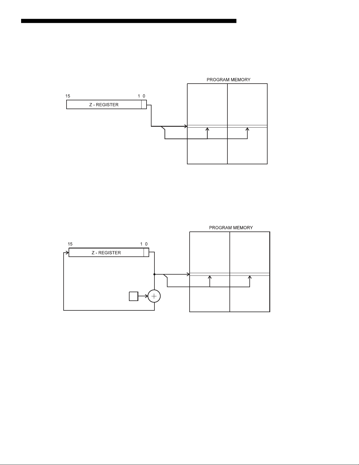
Program Memory Constant Addressing using the LPM, ELPM, and SPM Instructions
Figure 9. Program Memory Constant Addressing 0x0000 LSB FLASHEND
Constant byte address is specified by the Z-register contents. The 15 MSBs select word address. For LPM, the LSB selects
low byte if cleared (LSB = 0) or high byte if set (LSB = 1). For SPM, the LSB should be cleared. If ELPM is used, the RAMPZ
Register is used to extend the Z-register.
Program Memory with Post-increment using the LPM Z+ and ELPM Z+ Instruction
Figure 10. Program Memory Addressing with Post-increment 0x0000 LSB 1 FLASHEND
Constant byte address is specified by the Z-register contents. The 15 MSBs select word address. The LSB selects low byte
if cleared (LSB = 0) or high byte if set (LSB = 1). If ELPM Z+ is used, the RAMPZ Register is used to extend the Z-register.
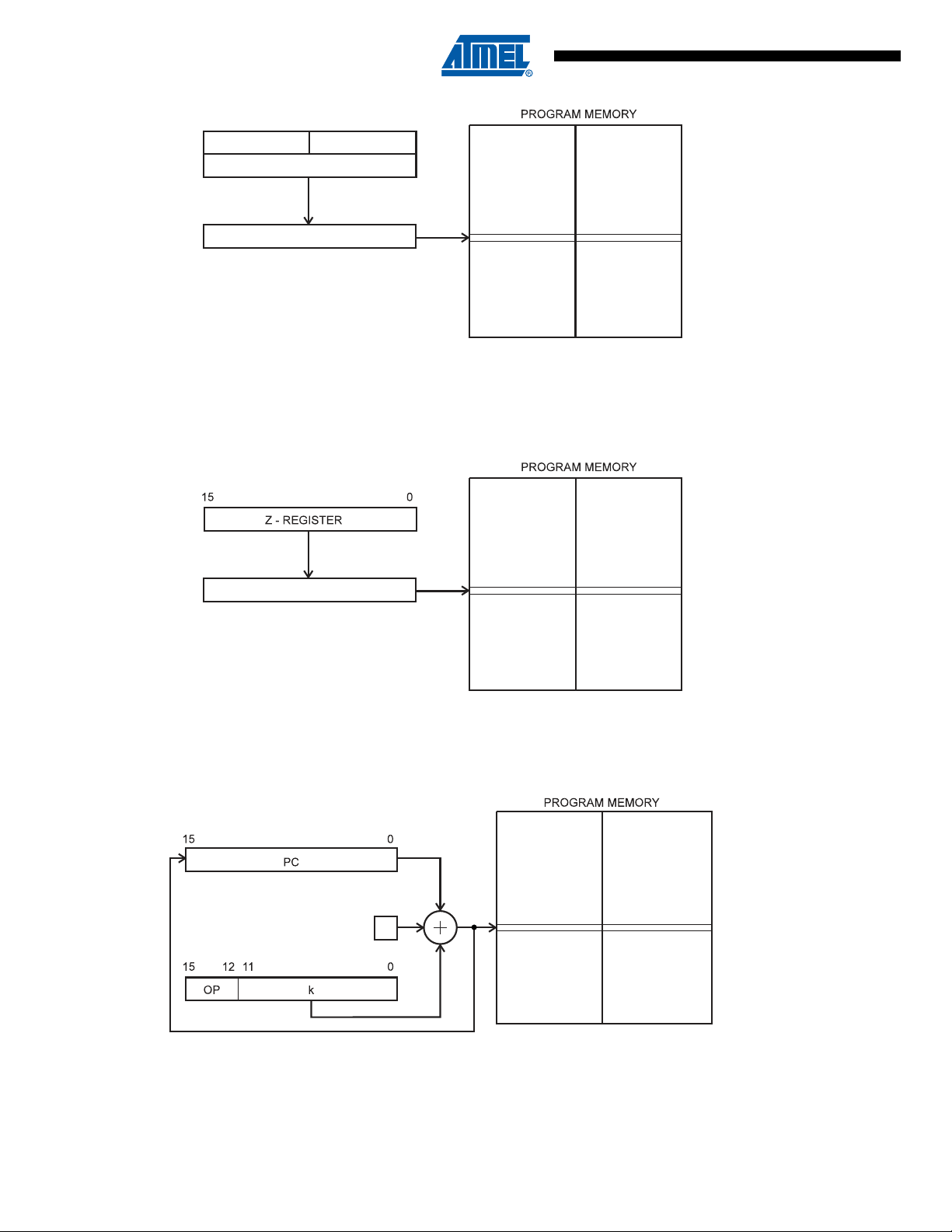
Direct Program Addressing, JMP and CALL
Figure 11. Direct Program Memory Addressing lOMoAR cPSD| 58583460 31 16 0x0000 OP 6 MSB 16 LSB 15 0 21 0 PC FLASHEN D
Program execution continues at the address immediate in the instruction word.
Indirect Program Addressing, IJMP and ICALL
Figure 12. Indirect Program Memory Addressing 0x0000 15 0 PC FLASHEN D
Program execution continues at address contained by the Z-register (i.e., the PC is loaded with the contents of the Zregister).
Relative Program Addressing, RJMP and RCALL
Figure 13. Relative Program Memory Addressing 0x0000 1 FLASHEND
Program execution continues at address PC + k + 1. The relative address k is from -2048 to 2047. lOMoAR cPSD| 58583460 AVR Instruction Set
Conditional Branch Summary Test Boolean Mnemonic Complementary Boolean Mnemonic Comment Rd > Rr Z•(N ⊕ V) = 0 BRLT(1) Rd ≤ Rr Z+(N ⊕ V) = 1 BRGE* Signed Rd Rr (N ⊕ V) = 0 BRGE Rd < Rr (N ⊕ V) = 1 BRLT Signed Rd = Rr Z = 1 BREQ Rd ≠ Rr Z = 0 BRNE Signed Rd ≤ Rr Z+(N ⊕ V) = 1 BRGE(1) Rd > Rr Z•(N ⊕ V) = 0 BRLT* Signed Rd < Rr (N ⊕ V) = 1 BRLT Rd ≥ Rr (N ⊕ V) = 0 BRGE Signed Rd > Rr C + Z = 0 BRLO(1) Rd ≤ Rr C + Z = 1 BRSH* Unsigned Rd Rr C = 0 BRSH/BRCC Rd < Rr C = 1 BRLO/BRCS Unsigned Rd = Rr Z = 1 BREQ Rd ≠ Rr Z = 0 BRNE Unsigned Rd ≤ Rr C + Z = 1 BRSH(1) Rd > Rr C + Z = 0 BRLO* Unsigned Rd < Rr C = 1 BRLO/BRCS Rd ≥ Rr C = 0 BRSH/BRCC Unsigned Carry C = 1 BRCS No carry C = 0 BRCC Simple Negative N = 1 BRMI Positive N = 0 BRPL Simple Overflow V = 1 BRVS No overflow V = 0 BRVC Simple Zero Z = 1 BREQ Not zero Z = 0 BRNE Simple Note:
1. Interchange Rd and Rr in the operation before the test, i.e., CP Rd,Rr → CP Rr,Rd lOMoAR cPSD| 58583460
Complete Instruction Set Summary
Instruction Set Summary #Clocks XMEGA Mnemonics Operands Description Operation Flags #Clocks
Arithmetic and Logic Instructions ADD Rd, Rr Add without Carry Rd ← Rd + Rr Z,C,N,V,S,H 1 ADC Rd, Rr Add with Carry Rd ← Rd + Rr + C Z,C,N,V,S,H 1 ADIW(1) Rd, K Add Immediate to Word Rd ← Rd + 1:Rd + K Z,C,N,V,S 2 SUB Rd, Rr Subtract without Carry Rd ← Rd - Rr Z,C,N,V,S,H 1 SUBI Rd, K Subtract Immediate Rd ← Rd - K Z,C,N,V,S,H 1 SBC Rd, Rr Subtract with Carry Rd ← Rd - Rr - C Z,C,N,V,S,H 1 SBCI Rd, K Subtract Immediate with Carry Rd ← Rd - K - C Z,C,N,V,S,H 1 SBIW(1) Rd, K Subtract Immediate from Word Rd + 1:Rd ← Rd + 1:Rd - K Z,C,N,V,S 2 AND Rd, Rr Logical AND Rd ← Rd • Rr Z,N,V,S 1 ANDI Rd, K Logical AND with Immediate Rd ← Rd • K Z,N,V,S 1 OR Rd, Rr Logical OR Rd ← Rd v Rr Z,N,V,S 1 ORI Rd, K Logical OR with Immediate Rd ← Rd v K Z,N,V,S 1 EOR Rd, Rr Exclusive OR Rd ← Rd ⊕ Rr Z,N,V,S 1 COM Rd One’s Complement Rd ← $FF - Rd Z,C,N,V,S 1 NEG Rd Two’s Complement Rd ← $00 - Rd Z,C,N,V,S,H 1 SBR Rd,K Set Bit(s) in Register Rd ← Rd v K Z,N,V,S 1 CBR Rd,K Clear Bit(s) in Register Rd ← Rd • ($FFh - K) Z,N,V,S 1 INC Rd Increment Rd ← Rd + 1 Z,N,V,S 1 lOMoAR cPSD| 58583460 AVR Instruction Set DEC Rd Decrement Rd ← Rd - 1 Z,N,V,S 1 TST Rd Test for Zero or Minus Rd ← Rd • Rd Z,N,V,S 1 CLR Rd Clear Register Rd ← Rd ⊕ Rd Z,N,V,S 1 SER Rd Set Register Rd ← $FF None 1 MUL(1) Rd,Rr Multiply Unsigned R1:R0 ← Rd x Rr (UU) Z,C 2 MULS(1) Rd,Rr Multiply Signed R1:R0 ← Rd x Rr (SS) Z,C 2 MULSU(1) Rd,Rr Multiply Signed with Unsigned R1:R0 ← Rd x Rr (SU) Z,C 2 FMUL(1) Rd,Rr Fractional Multiply Unsigned R1:R0 ← Rd x Rr<<1 (UU) Z,C 2 FMULS(1) Rd,Rr Fractional Multiply Signed R1:R0 ← Rd x Rr<<1 (SS) Z,C 2 FMULSU(1) Rd,Rr
Fractional Multiply Signed with R1:R0 ← Rd x Rr<<1 (SU) Z,C 2 Unsigned DES K Data Encryption if (H = 0) then R15:R0 ← Encrypt(R15:R0, 1/2
else if (H = 1) then R15:R0 ← K) Decrypt(R15:R0, K) Branch Instructions RJMP k Relative Jump PC ← PC + k + 1 None 2 IJMP(1) Indirect Jump to (Z) PC(15:0) ← Z, None 2 PC(21:16) ← 0 EIJMP(1) Extended Indirect Jump to (Z) PC(15:0) ← Z, None 2 PC(21:16) ← EIND JMP(1) k Jump PC ← k None 3 #Clocks XMEGA Mnemonics Operands Description Operation Flags #Clocks RCALL k Relative Call Subroutine PC ← PC + k + 1 None 3 / 4(3)(5) 2 / 3(3) ICALL(1) ← Z, 3 / 4(3) 2 / 3(3) Indirect Call to (Z) PC(15:0) PC(21:16) ← 0 None EICALL(1) Extended Indirect Call to (Z) PC(15:0) ← Z, None 4 (3) 3 (3) PC(21:16) ← EIND CALL(1) k call Subroutine PC ← k None 4 / 5(3) 3 / 4(3) RET Subroutine Return PC ← STACK None 4 / 5(3) lOMoAR cPSD| 58583460 RETI Interrupt Return PC ← STACK I 4 / 5(3) CPSE Rd,Rr Compare, Skip if Equal
if (Rd = Rr) PC ← PC + 2 or 3 None 1 / 2 / 3 CP Rd,Rr Compare Rd - Rr Z,C,N,V,S,H 1 CPC Rd,Rr Compare with Carry Rd - Rr - C Z,C,N,V,S,H 1 CPI Rd,K Compare with Immediate Rd - K Z,C,N,V,S,H 1 SBRC Rr, b
Skip if Bit in Register Cleared
if (Rr(b) = 0) PC ← PC + 2 or 3 None 1 / 2 / 3 SBRS Rr, b Skip if Bit in Register Set
if (Rr(b) = 1) PC ← PC + 2 or 3 None 1 / 2 / 3 SBIC A, b
Skip if Bit in I/O Register Cleared
if (I/O(A,b) = 0) PC ← PC + 2 or 3 None 1 / 2 / 3 2 / 3 / 4 SBIS A, b
Skip if Bit in I/O Register Set
If (I/O(A,b) =1) PC ← PC + 2 or 3 None 1 / 2 / 3 2 / 3 / 4 BRBS s, k Branch if Status Flag Set
if (SREG(s) = 1) then PC ← PC + k + 1 None 1 / 2 BRBC s, k Branch if Status Flag Cleared
if (SREG(s) = 0) then PC ← PC + k + 1 None 1 / 2 BREQ k Branch if Equal
if (Z = 1) then PC ← PC + k + 1 None 1 / 2 BRNE k Branch if Not Equal
if (Z = 0) then PC ← PC + k + 1 None 1 / 2 BRCS k Branch if Carry Set
if (C = 1) then PC ← PC + k + 1 None 1 / 2 BRCC k Branch if Carry Cleared
if (C = 0) then PC ← PC + k + 1 None 1 / 2 BRSH k Branch if Same or Higher
if (C = 0) then PC ← PC + k + 1 None 1 / 2 BRLO k Branch if Lower
if (C = 1) then PC ← PC + k + 1 None 1 / 2 BRMI k Branch if Minus
if (N = 1) then PC ← PC + k + 1 None 1 / 2 BRPL k Branch if Plus
if (N = 0) then PC ← PC + k + 1 None 1 / 2 BRGE k Branch if Greater or Equal, if (N ⊕ V= 0) then PC ← PC + k + 1 None 1 / 2 Signed BRLT k Branch if Less Than, Signed if (N ⊕ V= 1) then PC ← PC + k + 1 None 1 / 2 BRHS k Branch if Half Carry Flag Set
if (H = 1) then PC ← PC + k + 1 None 1 / 2 BRHC k
Branch if Half Carry Flag Cleared
if (H = 0) then PC ← PC + k + 1 None 1 / 2 BRTS k Branch if T Flag Set
if (T = 1) then PC ← PC + k + 1 None 1 / 2 lOMoAR cPSD| 58583460 AVR Instruction Set BRTC k Branch if T Flag Cleared
if (T = 0) then PC ← PC + k + 1 None 1 / 2 BRVS k
Branch if Overflow Flag is Set
if (V = 1) then PC ← PC + k + 1 None 1 / 2 BRVC k Branch if Overflow Flag is
if (V = 0) then PC ← PC + k + 1 None 1 / 2 Cleared BRIE k Branch if Interrupt Enabled
if (I = 1) then PC ← PC + k + 1 None 1 / 2 BRID k Branch if Interrupt Disabled
if (I = 0) then PC ← PC + k + 1 None 1 / 2
Data Transfer Instructions MOV Rd, Rr Copy Register Rd ← Rr None 1 MOVW(1) Rd, Rr Copy Register Pair Rd+1:Rd ← Rr+1:Rr None 1 LDI Rd, K Load Immediate Rd ← K None 1 LDS(1) Rd, k Load Direct from data space Rd ← (k) None 1(5)/2(3) 2(3)(4) LD(2) Rd, X Load Indirect Rd ← (X) None 1(5)2(3) 1(3)(4) #Clocks XMEGA Mnemonics
Operands Description Operation Flags #Clocks LD(2) Rd ← (X) 2(3) 1(3)(4) Rd, X+
Load Indirect and Post-Increment X ← X + 1 None LD(2) ← X - 1 (X) 2(3)/3(5) 2(3)(4) Rd, -X
Load Indirect and Pre-Decrement X ← X - 1, None Rd ← (X) ← LD(2) Rd, Y Load Indirect Rd ← (Y) ← (Y) None 1(5)/2(3) 1(3)(4) LD(2) Rd, Y+
Load Indirect and Post-Increment Rd ← (Y) None 2(3) 1(3)(4) Y ← Y + 1 LD(2) Y ← Y - 1 (Y) 2(3)/3(5) 2(3)(4) Rd, -Y
Load Indirect and Pre-Decrement Rd ← None LDD(1) Rd, Y+q
Load Indirect with Displacement Rd ← (Y + q) None 2(3) 2(3)(4) LD(2) Rd, Z Load Indirect Rd ← (Z) None 1(5)/2(3) 1(3)(4) LD(2) Rd ← (Z), 2(3) 1(3)(4) Rd, Z+
Load Indirect and Post-Increment Z ← Z+1 None LD(2) Rd, -Z
Load Indirect and Pre-Decrement Z ← Z - 1, (Z) None 2(3)/3(5) 2(3)(4) Rd ← LDD(1) Rd, Z+q
Load Indirect with Displacement Rd ← (Z + q) None 2(3) 2(3)(4) STS(1) k, Rr Store Direct to Data Space (k) ← Rd None 1(5)/2(3) 2(3) ST(2) X, Rr Store Indirect (X) ← Rr None 1(5)/2(3) 1(3) lOMoAR cPSD| 58583460 ST(2) X+, Rr
Store Indirect and Post-Increment (X) ← Rr, X None 1(5)/2(3) 1(3) X ← + 1 ST(2) X ← X - 1, 2(3) 2(3) -X, Rr
Store Indirect and Pre-Decrement (X) ← Rr None ST(2) Y, Rr Store Indirect (Y) ← Rr None 1(5)/2(3) 1(3) ST(2) Y+, Rr
Store Indirect and Post-Increment (Y) ← Rr, Y None 1(5)/2(3) 1(3) Y ← + 1 ST(2) Y ← Y - 1, 2(3) 2(3) -Y, Rr
Store Indirect and Pre-Decrement (Y) ← Rr None STD(1) Y+q, Rr
Store Indirect with Displacement (Y + q) ← Rr None 2(3) 2(3) ST(2) Z, Rr Store Indirect (Z) ← Rr None 1(5)/2(3) 1(3) ST(2) (Z) ← Rr 1(5)/2(3) 1(3) Z+, Rr
Store Indirect and Post-Increment Z ← Z + 1 None ST(2) -Z, Rr
Store Indirect and Pre-Decrement Z ← Z - 1 None 2(3) 2(3) STD(1) Z+q,Rr
Store Indirect with Displacement (Z + q) ← Rr None 2(3) 2(3) LPM(1)(2) Load Program Memory R0 ← (Z) None 3 3 LPM(1)(2) Rd, Z Load Program Memory Rd ← (Z) None 3 3 LPM(1)(2) Rd, Z+ Load Program Memory and Rd ← (Z), Z None 3 3 PostIncrement Z ← + 1 ELPM(1) Extended Load Program Memory R0 ← (RAMPZ:Z) None 3 ELPM(1) Rd, Z Extended Load Program Memory Rd ← (RAMPZ:Z) None 3 ELPM(1) Rd, Z+
Extended Load Program Memory and Rd ← (RAMPZ:Z), None 3 Post-Increment Z ← Z + 1 SPM(1) Store Program Memory (RAMPZ:Z) ← R1:R0 None - - SPM(1) Store Program Memory and (RAMPZ:Z) Z ← R1:R0, Z Z+ PostIncrement by 2 ← + 2 None - - IN Rd, A In From I/O Location Rd ← I/O(A) None 1 OUT A, Rr Out To I/O Location I/O(A) ← Rr None 1 PUSH(1) Rr Push Register on Stack STACK ← Rr None 2 1(3) POP(1) Rd Pop Register from Stack Rd ← STACK None 2 2(3) #Clocks XMEGA Mnemonics
Operands Description Operation Flags #Clocks
Bit and Bit-test Instructions lOMoAR cPSD| 58583460 AVR Instruction Set LSL Rd Logical Shift Left Rd(n+1) ← Rd(n), Z,C,N,V,H 1 Rd(0) ← 0, C ← Rd(7) LSR Rd Logical Shift Right Rd(n) ← Rd(n+1), Z,C,N,V 1 Rd(7) ← 0, C ← Rd(0) ROL Rd Rotate Left Through Carry Rd(0) ← C, Z,C,N,V,H 1 Rd(n+1) ← Rd(n), C ← Rd(7) ROR Rd Rotate Right Through Carry Rd(7) ← C, Z,C,N,V 1 Rd(n) ← Rd(n+1), C ← Rd(0) ASR Rd Arithmetic Shift Right Rd(n) ← Rd(n+1), n=0..6 Z,C,N,V 1 SWAP Rd Swap Nibbles Rd(3..0) ↔ Rd(7..4) None 1 BSET s Flag Set SREG(s) ← 1 SREG(s) 1 BCLR s Flag Clear SREG(s) ← 0 SREG(s) 1 SBI A, b Set Bit in I/O Register I/O(A, b) ← 1 None 1(5)2 1 CBI A, b Clear Bit in I/O Register I/O(A, b) ← 0 None 1(5)/2 1 BST Rr, b Bit Store from Register to T T ← Rr(b) T 1 BLD Rd, b Bit load from T to Register Rd(b) ← T None 1 SEC Set Carry C ← 1 C 1 CLC Clear Carry C ← 0 C 1 SEN Set Negative Flag N ← 1 N 1 CLN Clear Negative Flag N ← 0 N 1 SEZ Set Zero Flag Z ← 1 Z 1 CLZ Clear Zero Flag Z ← 0 Z 1 SEI Global Interrupt Enable I ← 1 I 1 CLI Global Interrupt Disable I ← 0 I 1 SES Set Signed Test Flag S ← 1 S 1 CLS Clear Signed Test Flag S ← 0 S 1 lOMoAR cPSD| 58583460 SEV
Set Two’s Complement Overflow V ← 1 V 1 CLV Clear Two’s Complement V ← 0 V 1 Overflow SET Set T in SREG T ← 1 T 1 CLT Clear T in SREG T ← 0 T 1 SEH Set Half Carry Flag in SREG H ← 1 H 1 CLH Clear Half Carry Flag in SREG H ← 0 H 1
MCU Control Instructions BREAK(1) Break
(See specific descr. for BREAK) None 1 NOP No Operation None 1 SLEEP Sleep
(see specific descr. for Sleep) None 1 WDR Watchdog Reset (see specific descr. for WDR) None 1
Notes: 1. This instruction is not available in al devices. Refer to the device specific instruction set summary.
2. Not all variants of this instruction are available in all devices. Refer to the device specific instruction set summary.
3. Cycle times for Data memory accesses assume internal memory accesses, and are not valid for accesses via the externalRAM interface.
4. One extra cycle must be added when accessing Internal SRAM.
5. Number of clock cycles for ATtiny10. lOMoAR cPSD| 58583460 AVR Instruction Set ADC – Add with Carry Description:
Adds two registers and the contents of the C Flag and places the result in the destination register Rd. Operation: (i) Rd ← Rd + Rr + C Syntax: Operands: Program Counter: (i) ADC Rd,Rr
0 ≤ d ≤ 31, 0 ≤ r ≤ 31 PC ← PC + 1 16-bit Opcode: 0001 11rd dddd rrrr
Status Register (SREG) Boolean Formula: I T H S V N Z C – – ⇔ ⇔ ⇔ ⇔ ⇔ ⇔ H: Rd3•Rr3+Rr3•R3+R3•Rd3
Set if there was a carry from bit 3; cleared otherwise S: N ⊕ V, For signed tests. V: Rd7•Rr7•R7+Rd7•Rr7•R7
Set if two’s complement overflow resulted from the operation; cleared otherwise. N: R7
Set if MSB of the result is set; cleared otherwise. Z:
R7• R6 •R5• R4 •R3 •R2 •R1 •R0
Set if the result is $00; cleared otherwise. C: Rd7•Rr7+Rr7•R7+R7•Rd7
Set if there was carry from the MSB of the result; cleared otherwise.
R (Result) equals Rd after the operation. Example: ; Add R1:R0 to R3:R2 add r2,r0 ; Add low byte adc r3,r1 ; Add with carry high byte Words: 1 (2 bytes) Cycles: 1 lOMoAR cPSD| 58583460
ADD – Add without Carry Description:
Adds two registers without the C Flag and places the result in the destination register Rd. Operation: (i) Rd ← Rd + Rr Syntax: Operands: Program Counter: (i) ADD Rd,Rr
0 ≤ d ≤ 31, 0 ≤ r ≤ 31 PC ← PC + 1 16-bit Opcode: 0000 11rd dddd rrrr
Status Register (SREG) and Boolean Formula: I T H S V N Z C – – ⇔ ⇔ ⇔ ⇔ ⇔ ⇔ H: Rd3•Rr3+Rr3•R3+R3•Rd3
Set if there was a carry from bit 3; cleared otherwise S: N ⊕ V, For signed tests. V: Rd7•Rr7•R7+Rd7•Rr7•R7
Set if two’s complement overflow resulted from the operation; cleared otherwise. N: R7
Set if MSB of the result is set; cleared otherwise. Z:
R7• R6 •R5• R4 •R3 •R2 •R1 •R0
Set if the result is $00; cleared otherwise. C:
Rd7 •Rr7 +Rr7 •R7+ R7 •Rd7
Set if there was carry from the MSB of the result; cleared otherwise.
R (Result) equals Rd after the operation. Example: add r1,r2 ; Add r2 to r1 (r1=r1+r2)
add r28,r28 ; Add r28 to itself (r28=r28+r28) Words: 1 (2 bytes) Cycles: 1 lOMoAR cPSD| 58583460 AVR Instruction Set
ADIW – Add Immediate to Word Description:
Adds an immediate value (0 - 63) to a register pair and places the result in the register pair. This instruction operates on the
upper four register pairs, and is well suited for operations on the pointer registers.
This instruction is not available in al devices. Refer to the device specific instruction set summary. Operation: (i) Rd+1:Rd ← Rd+1:Rd + K Syntax: Operands: Program Counter: (i)
ADIW Rd+1:Rd,K d ∈ {24,26,28,30}, 0 ≤ K ≤ 63 PC ← PC + 1 16-bit Opcode: 1001 0110 KKdd KKKK
Status Register (SREG) and Boolean Formula: I T H S V N Z C – – – ⇔ ⇔ ⇔ ⇔ ⇔ S: N ⊕ V, For signed tests. V: Rdh7 • R15
Set if two’s complement overflow resulted from the operation; cleared otherwise. N: R15
Set if MSB of the result is set; cleared otherwise. Z:
R15 •R14 •R13 •R12 •R11 •R10 •R9 •R8 •R7• R6• R5• R4• R3• R2 •R1• R0
Set if the result is $0000; cleared otherwise. C: R15 • Rdh7
Set if there was carry from the MSB of the result; cleared otherwise.
R (Result) equals Rdh:Rdl after the operation (Rdh7-Rdh0 = R15-R8, Rdl7-Rdl0=R7-R0). Example:
adiw r25:24,1 ; Add 1 to r25:r24
adiw ZH:ZL,63 ; Add 63 to the Z-pointer(r31:r30) Words: 1 (2 bytes) Cycles: 2 AND – Logical AND Description: lOMoAR cPSD| 58583460
Performs the logical AND between the contents of register Rd and register Rr and places the result in the destination register Rd. Operation: (i) Rd ← Rd • Rr Syntax: Operands: Program Counter: (i) AND Rd,Rr
0 ≤ d ≤ 31, 0 ≤ r ≤ 31 PC ← PC + 1 16-bit Opcode: 0010 00rd dddd rrrr
Status Register (SREG) and Boolean Formula: I T H S V N Z C – – – ⇔ 0 ⇔ ⇔ – S: N ⊕ V, For signed tests. V: 0 Cleared N: R7
Set if MSB of the result is set; cleared otherwise. Z:
R7 •R6 •R5 •R4 •R3• R2 •R1 •R0
Set if the result is $00; cleared otherwise.
R (Result) equals Rd after the operation. Example:
and r2,r3 ; Bitwise and r2 and r3, result in r2 ldi r16,1
; Set bitmask 0000 0001 in r16 and r2,r16 ; Isolate bit 0 in r2 Words: 1 (2 bytes) Cycles: 1
ANDI – Logical AND with Immediate Description:
Performs the logical AND between the contents of register Rd and a constant and places the result in the destination register Rd. Operation: (i) Rd ← Rd • K Syntax: Operands: Program Counter: (i) ANDI Rd,K
16 ≤ d ≤ 31, 0 ≤ K ≤ 255 PC ← PC + 1
Tài liệu liên quan:
-
Lab Report Template Môn Electrical Engineering | Trường Đại học Quốc tế, Đại học Quốc gia Thành phố Hồ Chí Minh
123 62 -
Lab 2 Kirchoff’s Current And Voltage Laws | Môn Electrical Engineering - Trường Đại học Quốc tế, Đại học Quốc gia Thành phố Hồ Chí Minh
99 50 -
Lab 7: FET Amplifier Study Guide | Môn Electrical Engineering - Trường Đại học Quốc tế, Đại học Quốc gia Thành phố Hồ Chí Minh
99 50 -
Review Midterm: Differential & Integration Amplifiers Concepts | Môn Electrical Engineering - Trường Đại học Quốc tế, Đại học Quốc gia Thành phố Hồ Chí Minh
108 54