Lab 7: FET Amplifier Study Guide | Môn Electrical Engineering - Trường Đại học Quốc tế, Đại học Quốc gia Thành phố Hồ Chí Minh
This lab introduces the operation of common source and common collector amplifier. You will know how to build a CE, CS circuits, measure the gain and compare to the theory calculation. Tài liệu được sưu tầm gồm 5 trang, giúp bạn ôn tập tốt hơn. Mời các bạn đón xem.
Môn: Electrical Engineering 8 tài liệu
Trường: Trường Đại học Quốc tế, Đại học Quốc gia Thành phố Hồ Chí Minh 2 K tài liệu
Tác giả:


Preview text:
lOMoAR cPSD| 58583460
INTERNATIONAL UNIVERSITY
SCHOOL OF ELECTRICAL ENGINEERING (EE) EE091 ELECTRONIC DEVICES LAB 7 FET AMPLIFIER
Full name: Nguyễn Trung Tín, Nguyễn
Thành Nhân Student number: EEEEIU22088, EEEEIU22073 I. OBJECTIVES
This lab introduces the operation of common source and common collector amplifier. You
will know how to build a CE, CS circuits, measure the gain and compare to the theory calculation II. MATERIAL AND EQUIPMENT 1. Oscilloscope 2. Power Supply 3. Multimeter 4. CD4007 lOMoAR cPSD| 58583460
INTERNATIONAL UNIVERSITY
SCHOOL OF ELECTRICAL ENGINEERING (EE) 5. Assorted Resistors 6. Assorted Capacitors III. THEORY
Before coming to the laboratory, student must review the definitions of threshold voltage VT,
device transconductance parameter 𝑘 , body effect coefficient 𝛾 and channel length
modulation coefficient parameter 𝜆.
Depending on the applied DC bias, MOSFETs have thre regions of operation:
• Cutoff region: 𝐼𝐷 = 0
NMOS: 𝑉𝐺𝑆 ≤ 𝑉𝑇𝑁
PMOS: 𝑉𝑆𝐺 ≤ 𝑉𝑇𝑃 • Triode (linear) region: 2
NMOS: 𝑉𝐷𝑆 < 𝑉𝑂𝑉 → 𝐼𝐷 = 𝑘′𝑊 (𝑉𝑂𝑉𝑉𝐷𝑆 − 𝑉 𝐷𝑆) , 𝑤ℎ𝑒𝑟𝑒 𝑉𝑂𝑉 = 𝑉𝐺𝑆 − 𝑉𝑇𝑁
𝑛 𝑊′ 𝐿 (𝑉𝑂𝑉𝑉𝐷𝑆 − 𝑉 𝑆𝐷22) , 𝑤ℎ𝑒𝑟𝑒 𝑉𝑂𝑉 = 𝑉𝑆𝐺 − |𝑉𝑇𝑃|
PMOS: 𝑉𝑆𝐷 < 𝑉𝑂𝑉 → 𝐼𝐷 = 𝑘 𝑝 𝐿 2
• Saturation region: 𝐼𝐷_𝑠𝑎𝑡. Neglecting the channel length modulation effect. NMOS:𝑉𝐷𝑆 𝑂𝑉 𝐷_𝑠𝑎𝑡
𝑘 𝑛 𝘍 𝑊 ( 𝐺𝑆 𝑇𝑁 )>2 𝑉 → 𝐼 2 𝐿
PMOS:𝑉𝑆𝐷 > 𝑉𝑂𝑉 → 𝐼𝐷_𝑠𝑎𝑡 = 𝑘
2𝘍 𝑝 𝐿𝑊 (𝑉𝐺𝑆 − 𝑉𝑇𝑃 )2 (S2)
1. Threshold voltage (𝑽𝑻) he voltage at which the surface inversion layer just forms
is called threshold voltage (𝑉𝑇). The inversion layer region is an extremely shallow layer,
existing as a charge sheet directly below the gate. AT 𝑉𝐺 exceeds the threshold voltage 𝑉𝑇𝑁,
the surface has inverted from the p-type polarity of original substrate to an n-type. For the
enhance-mode, 𝑉𝑇𝑁 >
0 𝑎𝑛𝑑 𝑉𝑇𝑃 < 0.
2. Transconductance parameters
𝑘 𝑎𝑛𝑑 𝑘′ are called transconductance parameters, both have units of 𝐴/𝑉2. The 𝑘 can be
estimated as the slope of √𝐼𝐷 from equation (S1) or equation (S2).
3. Body effect coefficient 𝜸
When a non-zero substrate bias voltage (𝑉𝑆𝐵) are applied. It has a huge effect on the
threshold voltage, thus introduce the body effect coefficiet 𝜸, which can be found from: lOMoAR cPSD| 58583460
INTERNATIONAL UNIVERSITY
SCHOOL OF ELECTRICAL ENGINEERING (EE) 𝑉𝑇 − 𝑉𝑇0 𝛾 = (G1)
√|2𝜙𝐹| + 𝑉𝑆𝐵 − √|2𝜙𝐹|
Where 𝑉𝑇: threshold voltage when a non-zero 𝑉𝑆𝐵 is applied. 𝑉𝑇0: threshold voltage
when 𝑉𝑆𝐵 = 0 𝑉, 𝜙𝐹: substrate Fermi potential.
Note that the substrate bias coefficient is positive in NMOS and negative in PMOS.
4. Channel length modulation coefficient parameter
Without neglecting the channel length modulation effect. The Equation(S1) or
Equation (S2) can be expained as follows: (S3) 𝑘
𝐼𝐷_𝑠𝑎𝑡 = 2 (𝑉𝐺𝑆 − 𝑉𝑇0)2 ∙ (1 + 𝜆 ∙ |𝑉𝐷𝑆|)
The experiment mesurement of the 𝜆 requires different test circuit setup. The 𝑉𝐺𝑆 is set to 𝑉𝑇0
+ 1. The 𝑉𝐷𝑆 is chosen sufficiently large so that the transistor operates in the saturation mode.
The 𝐼𝐷_𝑠𝑎𝑡 is measured for two different drain voltage values, 𝑉𝐷𝑆1𝑎𝑛𝑑 𝑉𝐷𝑆2. Since the 𝑉𝐺𝑆 =
𝑉𝑇0 + 1, the ratio of the measured drain current values I𝐷1 𝑎𝑛𝑑 𝐼𝐷2 is:
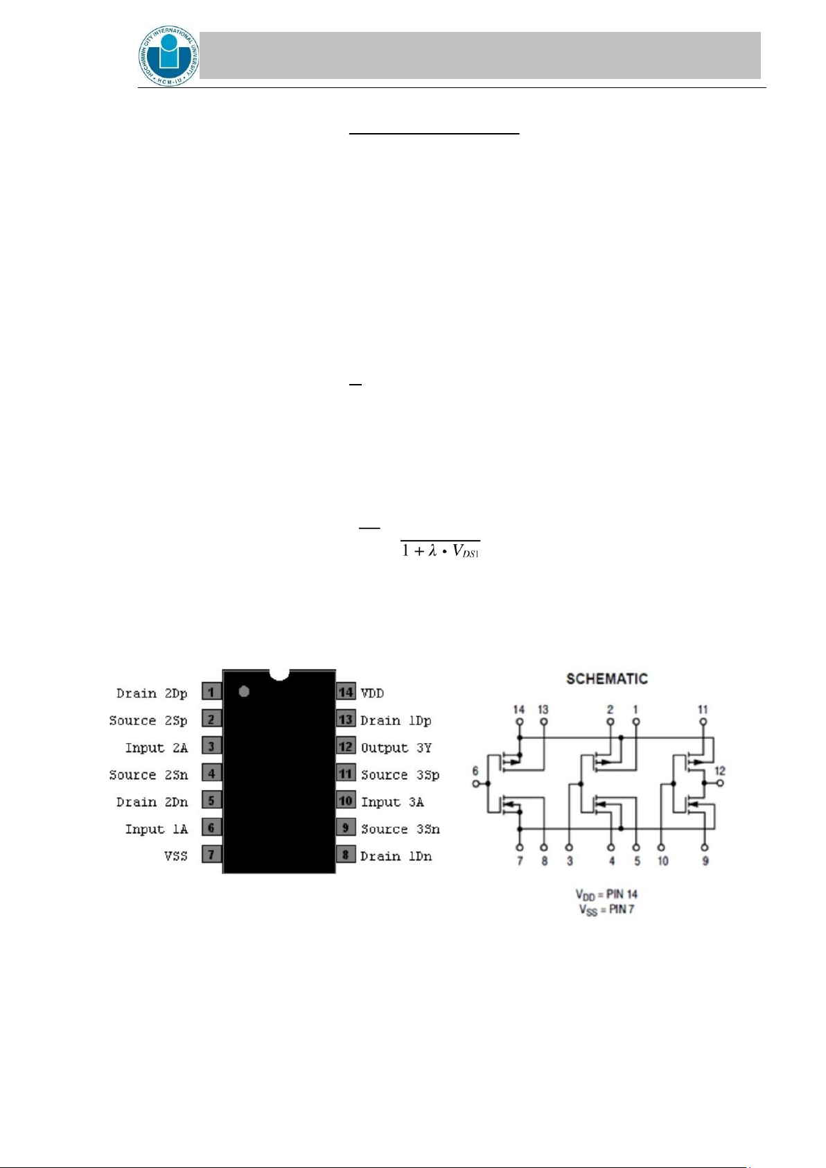
𝐼𝐷2 = 1 + 𝜆 ∙ 𝑉𝐷𝑆2 (S4) 𝐼𝐷1 5. CD4007 pinout
CD4007 is comprised of three n-channel and three p-channel enhancement MOS
transistors. The pinout of CD4007 is shown in Fig.1. IV. PROCEDURE
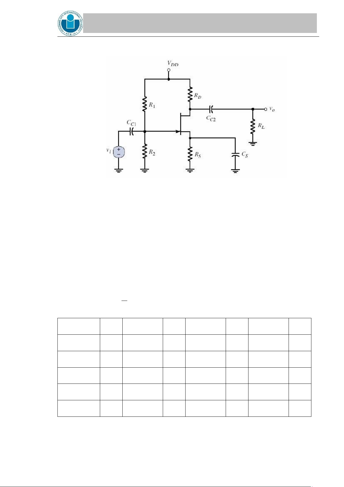
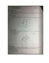
Common-Source Amplifier
The basic common-source (CS) circuit is shown in Figure 1. In comparison to the BJT
common-emitter amplifier, the FET amplifier has a much higher input impedance, but a
lower voltage gain. The voltage gain of the circuit can be expressed as: lOMoAR cPSD| 58583460
INTERNATIONAL UNIVERSITY
SCHOOL OF ELECTRICAL ENGINEERING (EE) Av = -gmRD Figure 1
Connect the circuit as shown in Figure 1.
Use Cc1 = 0.1μF, Cc2 = 1μF, Cs = 0.1 μF, RS = 1kΩ, RD = 47 kΩ, R1 = 200kΩ, R2=100 kΩ, VDD = 12V.
Apply a sinusoidal signal with frequency 1kHz, amplitude 0.4Vp-p a) Observe the output.
b) Capture both input and output waveforms.
c) Calculate the voltage gain.
d) Perform a frequency sweeping from 1Hz to 100KHz. Plot the frequency response ofvoltage gain (𝑉𝑜 dB. 𝑉𝑖) Frequency Gain Frequency Gain Frequency Gain Frequency Gain 100 1000 10,000 60,000 200 2000 20,000 70,000 400 3000 30,000 80,000 600 4000 40,000 90,000 800 5000 50,000 100,000
e) Connect Cc2 = 1μF to the Drain terminal. Capture the waveforms and measure the
gain. Then, connect the load resistor RL =1 kΩ, one pin is connected to the capacitor lOMoAR cPSD| 58583460
INTERNATIONAL UNIVERSITY
SCHOOL OF ELECTRICAL ENGINEERING (EE)
Cc2, the other pin is connected to the ground. Perform a parameter sweep on RL from
1 KOhm to 100 Kohm. observe the effects of R4 on the Vout of the circuit, and
comment on results. Assume that Vin does not change, compute the gains [𝑣𝑜𝑢𝑡] 𝑑𝐵 𝑣𝑖𝑛
based on the change the value RL . of 𝑅𝐿 𝑅 Gain Gain 𝐿 Gain Gain (Simulation) (Measurement) (Simulation) (Measurement) -23.05 -8.33 1𝑘Ω 5.6𝑘Ω -15.86 -6.83 2.2𝑘Ω 6.8𝑘Ω -12.54 -3.99 3.3𝑘Ω 10𝑘Ω -9.7 7.41 4.7𝑘Ω 100𝑘Ω
Tài liệu liên quan:
-
Lab Report Template Môn Electrical Engineering | Trường Đại học Quốc tế, Đại học Quốc gia Thành phố Hồ Chí Minh
122 61 -
Lab 2 Kirchoff’s Current And Voltage Laws | Môn Electrical Engineering - Trường Đại học Quốc tế, Đại học Quốc gia Thành phố Hồ Chí Minh
98 49 -
Review Midterm: Differential & Integration Amplifiers Concepts | Môn Electrical Engineering - Trường Đại học Quốc tế, Đại học Quốc gia Thành phố Hồ Chí Minh
108 54 -

Instruction Set Overview: Key Registers and Addressing Modes | Môn Electrical Engineering - Trường Đại học Quốc tế, Đại học Quốc gia Thành phố Hồ Chí Minh
96 48