Tài liệu về RF transceiver architectures for W-CDMA systems like UMTS môn Thu phát vô tuyến | Học viện Công Nghệ Bưu Chính Viễn Thông
The standardization phase for wideband CDMA systems like UMTS is running towards its finalization. Tài liệu được sưu tầm gồm 10 trang, giúp các bạn nắm vững kiến thức, rèn luyện kỹ năng và đạt được kết quả tốt trong học tập. Mời các bạn đón xem!
Môn: Thu phát vô tuyến (TEL1416) 10 tài liệu
Trường: Học viện Công Nghệ Bưu Chính Viễn Thông 1.8 K tài liệu
Tác giả:


Preview text:
RF Transceiver Architectures for W-
CDMA Systems Like UMTS: State of the Art and Future Trends
R. Weigel , L. Maurer , D. Pimingsdorfer , A. Springer
Institute for Communications and Information Engineering, University of Linz, Austria
DICE-Danube Integrated Circuit Engineering, Linz, Austria
{weigel, maurer, pimingsdorfer, springer}@mechatronik.uni-linz.ac.at Invited Paper
Abstract— The standardization phase for wideband
(WCDMA) systems follows. The last section gives a
CDMA systems like UMTS is running towards its
perspective of future trends in transceiver front-end
finalization. As is typical for mobile communication design for 3G systems.
systems standardizing, sufficient RF performance has
been assumed and most efforts have been put to baseband
In 1985 the ITU (International Telecommunications
issues. This is especially true for the pocket phone
Union) started work on 3G systems unter the acronym
transceivers the RF part of which is, although its
FPLMTS (Future Public Land Mobile Telephone
baseband part is much more complex in terms of number
of devices, still the bottleneck of the entire system. In the
System) which was later renamed to IMT-2000
RF concept engineering of today’s commercial products
(International Mobile Telecommunications) [1].
with their short time-to-market requirements, a
The key factors and main objectives for 3G systems
prediction of the needed RF performance by using RF
system simulation is meanwhile indispensable. This is in
include worldwide coverage and roaming incorporating
particular the case with third generation (3G) wireless
a satellite component, capacity and capability to serve
systems which, from the RF design point of view, are quite
more than 50% of the population [2], multimedia
different from 2G TDMA/FDMA systems due to the fact
service capability, high-speed access, low-cost
that the users are now separated in the power domain
operation, and integration of residential, office, and
(using codes) rather than being separated in the time
cellular services into a single system based on one piece
and/or frequency domain. The present work gives an
insight how to derive the transceiver requirements of 3G
of user equipment. Further issues are:
mobiles in terms recognizable by RF designers.
Packet access. This item is closely linked to the
Keywords—Transceivers, CDMA, Radio
above. Most of the traffic in 3G networks will originate
Communication, Spread Sprectrum Communications.
from data communications. Therefore, packet switched
communication must be provided in addition to a
circuit switched mode to ensure efficient resource I. INTRODUCTION
usage. This feature is or will be introduced already in
This work gives an introduction to transceiver design 2.5G systems like GPRS [3].
for third generation (3G) wireless communications
Evolution. The transition from 2G to 3G will be an
systems. We start with a review of the transition from
evolutionary path. In the beginning 3G systems and
second generation (2G) cellular systems to 3G systems.
services must coexist with todays 2G and 2.5G systems,
The following section introduces basic terms and
since no one (neither users nor network operators)
equations of the spread spectrum technique. The
would be able or willing to afford a hard transition from
relation between specific transceiver characteristics 2G or 2.5G to 3G.
like noise figure or linearity and testcases from the third
From the above mentioned items the basic demands for
generation partnership project (3GPP) specifications
data throughput over the air interface were identified as
are covered in the succeeding section. A review of
144kbps (preferably 384 kbps) with full coverage and
different receiver and transmitter architectures and their
high mobility of the user equipment (UE) and up to
suitability for wideband-code division multiple access
2Mbps for low mobility and coverage limited to high
traffic areas. These bit rates were harmonized to the
similar group was founded for the development of the
ISDN (Integrated Services Digital Network) 2B+D
cdma2000 based systems, termed 3GPP2 [8]. This
(144 kbps), H0 (384kbps), and H12 (1920 kbps)
activity is running in parallel to 3GPP and is
channels [1]. The general vision of 3G systems, is that coordinated with 3GPP [9].
they should basically ensure communications from
II. EVOLUTION FROM 2G TO 3G SYSTEMS
anywhere to anybody at any time.
Upon a request from the ITU for radio transmission
As pointed out before, there is already existing
technology (RTT) proposals, different regional
demand for data rates higher than the few kbps
standardization bodies submitted their proposals for
nowadays possible with 2G systems. With the
IMT2000 in 1998 [4]. Details of these proposals are
exception of the PDC system all 2G standards have
available at [5]. The vast majority of the submitted
provided add-on features supporting higher data rates
proposals were based on W-CDMA or at least
to account for this traffic demand. A review of these
contained a WCDMA component. During the
modes, commonly referred to as 2.5G systems, can be
evaluation of the different proposals by the ITU it
found in, e.g., [10]. If the 2.5G systems are fully
turned out that the vision of a global standard with a
deployed they will allow for data rates up to 384 kbps.
single radio interface was not realizable for 3G
With this the mobile units will evolve from mobile
systems. This was due to the different 2G technologies
phones to so-called smart phones including, e.g., PDA’s
used in the different regions in the world. It would have
(Personal Digital Assistants) to better support data
been impossible to find one technology as evolutionary
applications like email, Internet or location based
path for all existing 2G systems.
services. Also mobile Web panels are under
development. If the maximum data rate of 1Mbps in IMT-2000 Terrestrial
UMTS is available such demanding applications like Radio Interfaces
video conferencing could be supported. This will
introduce again a new generation of mobile terminals IMT-DS IMT-MC IMT-TC IMT-SC IMT-FT
capable of dealing with multimedia contents. Direct Multi Time Single Frequency Spread Carrier Code Carrier Time III. SPREAD SPECTRUM BASICS CDMA TDMA FDMA
The basic of spread spectrum (SS) technology is
given by Claude Shannon’s well known formula for the
Fig. 1. The set of IMT-2000 Terrestrial Radio Interfaces channel capacity [11]:
Therefore, a family concept was adopted and agreed
upon at the end of 1999 [6]. The five standards included (1)
in IMT-2000 are shown in Fig. 1. As IMT-DS (Direct
Spread) the UTRA FDD (UMTS Terrestrial Radio
C is the channel capacity in bps, W the bandwidth in
Access Frequency Division Duplex) mode was adopted
Hz, N the noise power and S the signal power.
in Europe and Japan, IMT-TC (Time-Code) is a
A spread spectrum system must meet two criteria:
combination of the UTRA TDD (Time Division
Duplex) (Europe and Japan) and the TD-SCDMA
The transmitted bandwidth is much greater than the
(China) proposals, cdma2000 (USA) is found in IMT-
bandwidth or rate of the information being sent.
MC (Multi Carrier), IMT-SC (Single Carrier)
The spreading signal must be independent of
corresponds to UWC136 (USA), and IMT-FT
information bearing signal (i.e. FM is not SS!).
(Frequency Time) is the European DECT proposal.
These five standards are now further developed in the
regional standardization bodies. For the W-CDMA
based technologies (IMT-DS and IMT-TC) the third
generation Partnership Project 3GPP was created [7]. A
An important reason for using SS is the linear
relatively complex structure of the RAKE-receiver and
dependency of the channel capacity C from the
the need of an accurate output power control in order to
bandwidth W in equation (1), whereas C increases only
deal with the near-far problem [12]. The wideband
with the logarithm of the signal to noise ration S/N.
nature of the signal also leads to the necessity of a
Furthermore, SS techniques have an inherent resistance
wideband modem and wideband baseband amplifier
against interference and jamming. Figure 2 gives an
stages. Furthermore, a fast and accurately working
explanation of this ability. Suppose a narrowband
automatic gain control (AGC) circuitry is a prerequisite
interferer is present in your received signal. Due to the
for an efficient handling of the multipath signal [13].
high correlation between the wanted signal (which was
SS systems can be described by a few equations and
spread in the transmitter by the same sequence) and the
terms. Important terms when talking about spread
locally generated code for despreading in the receiver,
spectrum are the so-called spreading factor SF and the
Fig. 2. An interfering signal is spread by a code sequence resulting in a lower power spectral density. The wanted signal level
is increased due to the high correlation of the spreading code and the signal.
the signal level increases. At the same time the
spreading gain SG. SF describes the ratio of the
interference signal is spread to a larger bandwidth and
information data rate (represented by the bit duration )
therefore the interference power in the receiver
to the rate of the spreading code (represented by the
bandwidth decreases. To gain this increase of the
chip duration ). This ratio ranges for, e.g., the 3GPP
wanted signal level, the locally generated code has to system from 4 to 512.
be exactly synchronized to the incoming wanted signal.
SS-systems can be classified in three main groups: (2)
Direct Sequence SS (DSSS): Spreading is done by a
multiplication of the data carrying signal with a code (3)
sequence of much larger bandwidth.
Frequency Hopping SS (FHSS): Spreading is
Let us denote the signal level before despreading the
accomplished by periodicly changing the carrier
chip energy to interference ratio ( /dB) and the signal
frequency. Chirp SS: Carrier frequency varies
level after despreading the bit energy to interference
continuously (usually linear) during a time interval.
ratio ( /dB). Than /dB, /dB and SG are related by
Most SS-systems are based on Direct Sequence-SS. For
that reason we will deal in the following exclusively (4)
with DSSS (also the term SS will refer to DSSS).
The factor OF/[dB] describes the degree of
The best known advantages of SS systems for
orthogonality between wanted user signal and
cellular system design include the possibility of
interference signal. The orthogonality factor (OF) for
selective addressing (Code Division Multiple Access
e.g. Gaussian noise equals 0 dB. Therefore, in a
(CDMA)) and the ability to eliminate the effect of
Gaussian noise environment the wanted user signal
multipath propagation by using a RAKE receiver in the
level is increased by an amount of SG dB. For perfectly
mobile station. Disadvantages incorporate the
orthogonal signals OF results to dB. Thus the choice of (6)
codes employed for the spreading of the user signals
greatly influences the overall performance of a CDMA
Inserting values for the Boltzmann constant k,
system. The orthogonality among the spreading codes
temperature T (300 K) and bandwidth B (3.84 MHz),
should be as large as possible.
equation (6) results in a tolerable noise figure NF of
At this point we emphasize once again that these
results are only valid for perfect synchronization of the (7)
received signal and the locally generated code for
despreading. It can be shown, that a timing error of,
B. Adjacent Channel Selectivity Testcase
e.g., one half of the chip time results in an SNR loss of
6 dB. Therefore obtaining initial synchronization and
Adjacent channel selectivity (ACS) is a measure of a
keeping the code synchronized by a code tracking loop
receiver’s ability to receive a W-CDMA signal at its
can be considered as key problems in SS system design.
assigned channel frequency in the presence of an
adjacent channel signal at a given frequency offset from
IV. TRANSCEIVER REQUIREMENTS AND
the center frequency of the assigned channel. Adjacent
3GPP FRONT-END TESTCASES
channel selectivity is the ratio of the receive filter
attenuation on the assigned channel frequency to the
The short explanation of some of the 3GPP testcases
receive filter attenuation on the adjacent channel(s).
below should give the reader an introduction of how RF
key parameters can be derived from specifications Power Spectral
given by 3GPP. The complete set of RF specific Density -52 dBm/3.84 MHz
testcases for the 3GPP FDD mode can be found in [14].
Further comments to these testcases are made in [15].
A. Reference Sensitivity Level Testcase -92,7 dBm/3,84 MHz
The reference sensitivity is the minimum receiver 10,3
input power measured at the antenna port at which the dB
bit error rate (BER) does not exceed a value of 10 . This DPCH_Ec=-103 dBm
testcase determines the tolerable noise figure of the
receiver front end. The cumulative value of the 5 MHz
incoming signal power is -106,7 dBm. The wanted user Wanted Adjacent
signal level before despreading is -117 dBm. The
reference channel is a 30ksps channel which yields an Channel Channel
SF of 128. According to equation (3) this result in a
value for SG of approximately 21dB. Let us assume
Fig. 3. Signal levels for the Adjacent Channel Selectivity
that the required bit energy to interference ratio is testcase.
5dB, the insertion loss (IL) for the baseband
The ACS shall be better than 33 dB. Simultaneously,
implementation is 2dB and the coding gain (CG) is
the bit error rate shall not exceed 10 for the following
4dB. Then the acceptable interference signal level after
test parameters (see Fig. 3). Received power spectral despreading (P ) result in:
density of the wanted signal at the terminal antenna
connector is -92,7dBm/3.84 MHz. The wanted user (5)
signal level before despreading is -103 dBm. The
symbol rate of the physical channel is 30ksps. This re-
Inserting values in equation (5) results in:
sults in an SF of 128 which yields a processing gain of
P =-117 dBm+21dB+4dB-5dB-2dB=-99 dBm.
approximately 21dB. The power spectral density of the
band limited white noise 5MHz away from the wanted
This leaves a margin for the front end noise figure channel P is -52dBm/3.84 MHz. (NF) of
We assume again that the required bit energy to
choice of the IF is a principal consideration in interference ratio
is 5dB, the insertion loss (IL)
heterodyne receiver design (see Fig. 5).
for the baseband implementation is 2dB and the coding
As the first mixer downconverts frequency bands
gain (CG) is 4dB. This leads us to an acceptable
symmetrically located above and below the local interference level P of
oscillator (LO) to the same center frequency, an image
reject filter in front of the mixer is needed. As depicted
in the left part of Fig. 5, the filter is designed to have a (8)
relatively small loss in the desired band and a large resulting in a value of
attenuation in the image band, two requirements that
can be simultaneously met if is sufficiently large. Thus,
a large IF relaxes the requirements for the image (9)
rejection filter, which is placed in front of the mixer
(see Fig. 4). On the other hand it complicates the design
If the adjacent channel interference signal is treated as
of the channel selection filter (right part of Fig. 5),
Gaussian noise like interference, the required adjacent
because of the higher IF. In today’s cellular systems the
channel selectivity (ACS) can be derived:
channel selection filtering is normally done with
surface acoustic wave (SAW) filters [18]. (10)
The equations used in this section exemplify of how
the signal levels are influenced by the despreading
operation and by interference sources. However, one
should always keep in mind that these results can only
serve as estimates. Further estimations such like the
above mentioned ones can be found in [16]. V. TRANSCEIVER DESIGN
Fig. 5. Image rejection and channel selection for the
A. General Considerations
heterodyne receiver structure.
Complexity, cost, power dissipation, and the number
Another interesting situation arises with an interferer
of external components have been the primary criteria
at . If this interferer experiences second-order distortion
in selecting transceiver architectures. As IC
and the LO contains a significant second harmonic,
technologies evolve, however, the relative importance
then a component at arises. This phe-
of each of these criteria changes, allowing approaches
that once seemed impractical to return as plausible
nomenon is called half-IF problem [19]. solutions [17].
A major advantage of the heterodyne receiver
structure is its adaptability to many different receiver
B. Receiver Architectures
requirements. That is why it has been the dominant
choice in RF systems for many decades. However, the B.1 Heterodyne Receiver
complexity of the structure and the need for a large
number of external components (e.g., the IF filter)
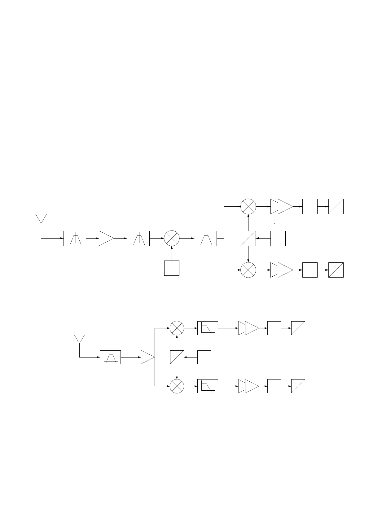
Figure 4 shows the heterodyne receiver structure.
make problems if a high level of integration is
This architecture first translates the signal band down
necessary. This is also the major drawback if costs are
to some intermediate frequency (IF), which is usually
concerned. Furthermore, amplification at some high IF
much lower than the initially received frequency band.
can cause high power consumption.
Channel select filtering is usually done at this IF, which
The IMT-2000 proposal specifies an operation mode
relaxes the requirements of the channel select filter. The
using two times or four times the base chiprate resulting
in a bandwidth of 7,68MHz or 15,36 MHz, respectively
other phasing method), otherwise the negative-
(multiband operation). On the other hand the handsets
frequency half-channel will fold over and superpose on
should also be able to receive GSM signals with a
to the positive-frequency half-channel [20].
bandwidth of approximately 200 kHz (multimode
The simplicity of this structure offers two important
operation). Due to the fixed receive bandwidth of the
advantages over a heterodyne counterpart. First the
heterodyne receiver structure caused by the external IF-
problem of image is circumvented because . As a result,
filter, these multimode and multiband capability can
no image filter is required. This may also simplify the
only be implemented by using a separate IF section for
LNA design, because there is no need for the LNA to
each mode. This would result in high costs and a
drive a 50 load, which is normally necessary when complex receiver structure.
dealing with image rejection filters. Second, the IF
SAW filter and subsequent downconversion stages are B.2 Homodyne Receiver
replaced with low-pass filters and baseband amplifiers
that are amenable to monolithic integration. The
The homodyne receiver structure (also called zeroIF
possibility of changing the bandwidth of the integrated
or direct-conversion architecture) entails vastly
low-pass filters (and thus changing the receiver
different issues from the heterodyne topology. Suppose
bandwidth) is a major advantage if multimode and
that the IF in a heterodyne receiver is reduced to zero.
multiband applications are concerned.
The LO will then translate the center of the desired VGA A Band Image Channel I D Select Reject Select Filter LNA Filter Filter 0 VCO 90 VCO A Q D
Fig.4.Heterodynereceiverstructure. Channel Select Filter VGA I A D Preselect filter LNA 0 VCO 90 A Q D
Fig. 6. Homodyne receiver structure.
channel to 0Hz, and the channel translated to the
On the other hand the zero-IF receiver topology
negative frequency half-axis becomes the image to the
entails a number of issues that do not exist or are not as
other half of the same channel translated to the positive
serious in a heterodyne receiver. Since in a homodyne
frequency half-axis. The downconverted signal must be
topology the downconverted band extends to zero
reconstituted by quadrature downconversion (or some
frequency, offset voltages can corrupt the signal and,
more importantly, saturate the following stages. There
possible because of the wideband nature of the signal.
are three main possibilities how DC-offsets are
A system level DC offset compensation approach is
generated. First, the isolation between the LO port and described in [22].
the inputs of the mixer and the LNA is not infinite.
I/Q mismatches are another critical issue for the
Therefore, a finite amount of feedthrough exists from
zeroIF receiver topology. Fortunately, pilot symbol
the LO port to the mixer or the LNA input. This “LO
assisted channel estimation is done in W-CDMA
leakage” arises from capacitive and substrate coupling
systems. Irrespective of the pilot symbols used (either
and, if the LO signal is provided externally, bond wire
the time multiplexed pilot symbols or the common pilot
couplings. This leakage signal is now mixed with the
signal), this estimation leads also to a correction of the
LO signal, thus producing a DC component at the mixer
I/Q phase and amplitude mismatch.
output. This phenomenon is called “self-mixing”. A
similar effect occurs if a large interferer leaks from the B.3 Digital-IF Receivers
LNA or mixer input to the LO port and is multiplied by
itself. A time varying DC offset is generated if the LO
In the heterodyne receiver architecture of Fig. 4 the
leaks to the antenna and is radiated and subsequently
second downconversion and subsequent filtering can be
reflected from moving objects back to the receiver.
done digitally. The principal issue in this approach is
Large amplitude modulated signals that are
the performance required from the ADC. To limit the
converted to the baseband section via second order
requirement on the ADC, a sufficiently low IF has to be
distortion of the IQ-mixers also lead to time varying
chosen, which makes it impossible to employ bandpass
DC offset. The spectral shape of this signal contains a
filtering to suppress the image frequency. Thus, an
significant component at DC accounting for
image suppression mixer has to be used. The image
approximately 50% of the energy. The rest of the
suppression feasible in today’s systems is limited to a
spurious signal extends to two times of the signal
range of 30-55 dB. Due to the high demands on the
bandwidth before downconverted by the second order
ADC and the image suppression mixer performance
nonlinearity of the mixers. The cause for the large
this architecture has not been used for terminal
signal content at DC is that every spectral component
applications. Nevertheless, it is utilized in base stations
of the incident interferer is coherently downconverted
where man channels must be received and processed
with itself to DC. In order to prevent this kind of DC simultaneously.
offset, a large second order intercept point (IP2) of the IQ-mixer is necessary.
C. Transmitter Architectures
3GPP compliant receivers need approximately 80dB
C.1 Direct Conversion Transmitter
gain. Most of this gain is contributed by the baseband
amplifiers. That means that even small DC offsets (in
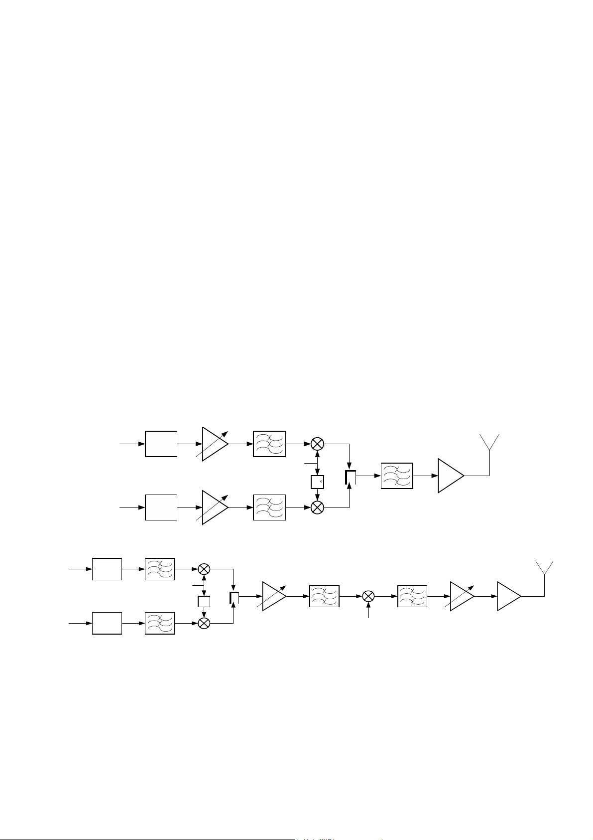
It the transmitted carrier frequency is equal to the
the range of several mV) at the mixer outputs may lead
local oscillator frequency, the architecture is called
to DC levels sufficient to saturate the analog to digital
“direct conversion”. In this case, modulation and converters (ADC).
upconversion occur in the same circuit. The
architecture in Fig. 7 suffers from an important
In time-division multiple access (TDMA) systems
drawback. Through a mechanism called “injection
idle time intervals can be used to carry out offset
pulling” or “injection locking” the transmit LO
cancellation. This would be a practical solution for the
spectrum is corrupted by the power amplifier (PA). The
3GPP-TDD mode. It can not be used for offset
problem worsens if the PA is turned on and off
cancellation in the FDD mode, because of the
periodically, as it is the case for the 3GPP-TDD mode.
continuous signal reception. Here, the natural solution
for DC offset cancellation is high-pass filtering. Since
Problems also arise if the system has to fulfil tight
the signal band extends from DC to approximately
requirements on output power range, which is usually
2MHz, a highpass filter with a cut-off frequency of
necessary in W-CDMA systems. Most of the gain has
several kHz results in an acceptable degradation of the
to be done in the baseband section, leading to high
system performance [21]. This approach is only
linearity requirements for the baseband filters and the
modulator. Furthermore, the LO lies always in the
a fully integrated Si-bipolar IF receiver and transmitter
transmit band, which causes high requirements on the
with on-chip synthesizer for use in third-generation
LO-RF isolation. I/Q phase mismatches are also an
WCDMA mobiles. Both devices in a small outline
issue when using direct upconversion. Even a low error
leadless package incorporate an on-chip IF synthesizer
in the phase shifting network may lead to a severe
with on-chip VCO tuning and tank as well as 6 /5 order
degradation of the error vector magnitude (EVM).
baseband filters and comply with ARIB W-CDMA and
UMTS standards. The IF-chips are fabricated with C.2 Heterodyne Transmitter
Infineon’s high frequency 0.4 m/25GHz silicon bipolar
process. IF receiver and IF transmitter die size is
The second possibility of signal upconversion, which
2.33x2.9 mm . The devices are designed for low
circumvents the problem of LO pulling in transmitters,
external component count and, together with the small
is to upconvert the baseband signal in two steps so that
package size, minimize the required board area of a
the PA output spectrum is far from the frequency of the
complete IF transceiver. The chips operate at 2.7-3.3V
VCO’s. An advantage of two-step upconversion over
supply, an ambient temperature range of -30 to +85, and
the direct conversion approach is that since quadrature
incorporate several power-down modes for efficient
modulation is performed at lower frequencies, I and Q
use in W-CDMA mobile stations. The W-CDMA IF
matching is superior. On the other hand, an IF filter (in
receiver includes two complete IF paths for antenna
most cellular applications again a SAW filter) is needed
diversity/service channel monitoring and a common
which can rise costs considerably.
LO generation and distribution. Each path features a
If high integration is an important feature, then both
variable gain amplifier with >95 dB gain range at an IF
heterodyne transmitters and receivers can cause
frequency of 318MHz, a quadrature demodulator and a
problems. Trying to find intermediate frequencies for
5 -order Chebyshev filter and 1 -order all-pass for the
the transmit and receive section, that do not lead to
differential I/Q outputs. The IF synthesizer includes a
spurious frequencies falling, e.g., in the receive band,
completely integrated on-chip VCO with integrated
may prove to be impossible. This is especially true, if
transformer and varactor diodes, tuning circuitry and
single chip transceivers are concerned.
on-chip voltage regulator for the VCO/buffer. A fixed I D/A AGC RF SAW LO PA ° 90 + Q D/A AGC
Fig. 7. Direct upconversion transmitter structure. I D/A IF SAW RF SAW LO IF AGC AGC PA 90 ° + Q D/A LO RF
Fig. 8. Heterodyne transmitter.
VI. CURRENT DEVELOPMENTS AND FUTURE TRENDS
PLL with reference divider, RF prescaler, lock detect
circuitry and three external elements for 3 -order loop
filter complete the on-chip synthesizer. The W-CDMA
The first operable UMTS IF transceiver front end
IF transmitter includes a 5 order active Butterworth
was published in Reference [23]. This paper describes
baseband pre-filter, a quadrature modulator, a variable
gain amplifier with >60 dB gain range at a fixed IF
architectures was given. Their suitability for the W-
frequency of 285MHz. The fully integrated VCO
CDMA system was evaluated and possible problems
operates at a frequency of 1520 MHz.
were addressed. The last section reviews the state-of-
the art and discusses future trends of W-CDMA
Most of the published work on receiver design is
transceiver design. Possible advances with respect to
based on the direct conversion topology. It seems that
improved devices, circuit topologies, and system-level
especially the need for high integration restricts the
architecture can make RF CMOS based transceivers a
receiver architecture to the zero-IF structure. Examples promising possibility.
can be found in [24][25][26][27][28]. All these
receivers are designed using standard BiCMOS
processes. An interesting option is the use of Si/Ge REFERENCES
bipolar technology for the receiver front end [29][30].
[1] T. Ojanperä and R. Prasad, Wideband CDMA for Third
This receiver incorporates an I/Q down conversion
Generation Mobile Communications. The Artech House
mixer, broad-band I/Q-generation, fully- integrated
Universal Personal Communications Series, Artech House, 1998.
VCO, dual-modulus prescaler, low-noise baseband
[2] P. Tagghol, B. G. Evans, E. Buracchini, R. D. Gaudenzi, G.
buffer and a blocking filter. Integrated in a 75GHz f
Gallinaro, J. H. Lee, and C. G. Kang, “Satellite UMTS/IMT–
BiCMOS technology with 35 m CMOS it draws 33mA
2000 W–CDMA Air Interfaces ,” IEEE Communications
from a 2.7V supply. Remarkable are the extremely low
Magazine, vol. 37, pp. 116–126, Sept. 1999.
LO leakage of -95dBm together with a high IIP2 of
[3] J. Cai and D. J. Goodman, “General Packet Radio Service in
GSM,” IEEE Communications Magazine, vol. 35, pp. 122–
55dBm. This results in very low DC offset values of 131, Oct. 1997.
less than 20 mV at the baseband output of the IC.
[4] P. Chaudhury, W. Mohr, and S. Onoe, “The 3GPP Proposal for
IMT–2000,” IEEE Communications Magazine, vol. 37, pp. With the continuing development of 72–81, Dec. 1999.
complementarymetal-oxide-semiconductor (CMOS)
[5] http://www.itu.int/imt/2_rad_devt/proposals/index-html.
components and processing techniques, CMOS
[6] ITU/99-22, “IMT–2000 Radio Interface Specifications
technology is also expected to become suitable for RF
Approved in ITU Meeting in Helsinki.” ITU Press Release, Nov.
applications within a few years. Advances with respect 1999.
to improved devices, circuit topologies, and system- [7] http://www.3gpp.org.
level architecture make CMOS a strong contender for [8] http://www.3gpp2.org.
implementing transceivers for the IMT-2000 global
[9] H. Holma and A. Toskala, WCDMA for UMTS. John Wiley &
wireless system [31]. RF CMOS seems to be a Sons, 2000.
promising approach, even though the performance of
[10] S. Nanda, K. Balachandran, and S. Kumar, “Adaptation
Techniques in Wireless Packet Data Services,” IEEE
some key components like PAs, VCOs and filters is not
Communications Magazine, vol. 38, no. 1, pp. 54–64, 2000.
sufficient yet. Considering the rapid development of RF
[11] C. E. Shannon, “Communication in the Presence of Noise,”
CMOS technology, however, some of these building
Proceedings of the IRE, vol. 37, no. 1, pp. 10–21, 1949.
blocks may become available within a few years. An
[12] M. K. Simon, J. K. Omura, R. A. Scholtz, and B. K. Levitt,
interesting project aimed at RF-CMOS design for W-
Spread Spectrum Communications Handbook. McGraw-Hill, Inc, 1985.
CDMA transceivers is described in Reference [32].
[13] R. C. Dixon, Radio Receiver Design. Marcel Dekker, Inc., New York, 1998. VII. CONCLUSION
[14] Technical Specification Group Radio Access Networks, “UE
Radio Transmission and Reception (FDD),” Tech. Rep. TS
25.101 V3.5.0, 3rd Generation Partnership Project, Dec.
A review of cellular phone transceiver concepts for 2000.
IMT 2000 system use was given. It was shown how [15] Technical Specification Group Terminals, “Radio
basic spread spectrum equations lead to an estimation
transmission and reception (FDD),” Tech. Rep. TS 34.121
of the transceiver system requirements. Examples
V3.3.0, 3rd Generation Partnership Project, Dec. 2000.
exhibit the influence of 3GPP testcases on key
[16] O. K. Jennsen, T. E. Kolding, C. R. Iversen, S. Laursen, R. V.
Reynisson, J. H. Mikkelsen, E. Pedersen, M. B. Jenner, and T.
parameters for the transceiver design. Furthermore, a
Larsen, “RF Receiver Requirements for 3G W–CDMA
review of the most popular receiver and transmitter
Mobile Equipment,” Microwave Journal, pp. 22–46, Feb. 2000. [17] B. Razavi, RF Microelectronics. Prentice Hall
communications engineering and emerging technologies
series, Prentice Hall, Inc., 1998.
[18] L. Maurer, W. Schelmbauer, H. Pretl, Z. Boos, R. Weigel, and
A. Springer, “Impact of IF-SAW Filtering on the Performance
of a W–CDMA Receiver,” in Ultrasonics 2000 Symposium, Oct. 2000.
[19] R. C. Sagers, “Intercept Point and Undesired Responses,”
IEEE Transactions on Vehicular Technology, vol. 32, pp. 121– 133, Feb. 1983.
[20] A. A. Abidi, “Direct–Conversion Radio Transceivers for
Digital Communications,” IEEE Journal of Solid–State
Circuits, vol. 30, pp. 1399–1410, Dec. 1995.
[21] J. H. Mikkelsen, T. E. Kolding, T. Larsen, T. Klingenbrunn,
K. I. Pedersen, and P. Mogensen, “Feasibility Study of DC
Offsett Filtering for UTRA–FDD/WCDMA Direct–
Conversion Receiver,” in IEEE NORCHIP Conference, pp. 34–39, Nov. 1999.
[22] H. Tsurumi, M. Soeya, H. Yoshida, T. Yamaji, H. Tanimoto,
and Y. Suzuki, “ System–Level Compensation Approach to
Overcome Signal Saturation, DC Offset, and 2nd–Order
Nonlinear Distortion in Linear Direct Conversion Receiver,”
IEICE Trans. Electron., vol. E82-C, pp. 708–716, May 1999.
[23] W. Thomann, J. Fenk, R. Hagelauer, and R. Weigel, “Fully
Integrated W–CDMA IF Receiver and Transmitter including
IF Synthesizer and on–chip VCO for UMTS Mobiles,” in
IEEE Bipolar/BICMOS Technology Meeting, 2000.
[24] K. Itoh, T. Katsura, H. Nagano, T. Yamaguchi, and Y. Hamade,
“2 GHz Band Even Order Harmonic Type Direct Conversion
Receiver with ABB–IC for W–CDMA Mobile Terminal,” in
Microwave Symposium Digest, pp. 1957– 1960, 2000.
[25] A. Pärssinen, J. Jussila, J. Ryynänen, L. Sumanen, and K.
Halonen, “A Wide–Band Direct Conversion Receiver for
WCDMA Applications,” in 1999 IEEE International
SolidState Circuits Conference, pp. 220–221, 1999.
[26] A. Pärssinen, J. Jussila, J. Ryynänen, L. Sumanen, and K. A.
I. Halonen, “A 2–GHz Wide–Band Direct Conversion
Receiver for WCDMA Applications,” IEEE Journal of Solid–
State Circuits, vol. 34, pp. 1893–1903, Dec. 1999.
[27] B. Sam, “Direct Conversion Receiver for Wide-band
CDMA,” in Spring Wireless Symposium, 2000.
[28] M. Goldfarb, W. Palmer, T. Murphy, R. Clarke, B. Gilbert, K.
Itoh, T. Katsura, R. Hayashi, and H. Nagano, “Analog
Baseband IC for Use in Direct Conversion W–CDMA
Receivers,” in RFIC Symposium, pp. 79–82, 2000.
[29] H. Pretl, W. Schelmbauer, B. Adler, L. Maurer, J. Fenk, and
R. Weigel, “A SiGe–Bipolar Down–Conversion Mixer for a
UMTS Zero–IF Receiver,” in IEEE Bipolar/BICMOS
Technology Meeting, pp. 40–43, 2000.
[30] H. Pretl, W. Schelmbauer, L. Maurer, H. Westermayr, R.
Weigel, B. U. Klepser, B. Adler, and J. Fenk, “A W– CDMA
Zero–IF Front–End for UMTS in a 75 GHz SiGe BiCMOS
Technology.” to be published.
[31] J. H. Mikkelsen, T. E. Kolding, and T. Larsen, “RF CMOS
Circuits Target IMT–2000 Applications,” Microwaves & RF, pp. 99–107, 1998.
[32] http://www.iis.ee.ethz.ch/nwp/lemon/lemon.html.
Tài liệu liên quan:
-
Bài tập quy hoạch mạng hệ thống thu phát vô tuyến môn Thu phát vô tuyến | Học viện Công Nghệ Bưu Chính Viễn Thông
120 60 -
Tài liệu về Transmit diversity in 3G CDMA systems môn Thu phát vô tuyến | Học viện Công Nghệ Bưu Chính Viễn Thông
118 59 -
Chapter 6 WCDMA môn Thu phát vô tuyến | Học viện Công Nghệ Bưu Chính Viễn Thông
138 69 -
Tài liệu về Introduction to UMTS device testing môn Thu phát vô tuyến | Học viện Công Nghệ Bưu Chính Viễn Thông
119 60