Lab 4 - Exploring Operational Amplifiers and Their Configurations | Môn Principles of EE 1 - Trường Đại học Quốc tế, Đại học Quốc gia Thành phố Hồ Chí Minh
Lab 4 - Exploring Operational Amplifiers and Their Configurations Môn Principles of EE 1. Tài liệu được sưu tầm gồm 13 trang, giúp bạn ôn tập tốt hơn. Mời các bạn đón xem.
Môn: Principles of EE 1 10 tài liệu
Trường: Trường Đại học Quốc tế, Đại học Quốc gia Thành phố Hồ Chí Minh 2 K tài liệu
Tác giả:


Preview text:
lOMoAR cPSD| 58097008 INTERNATIONAL UNIVERSITY
SCHOOL OF ELECTRICAL ENGINEERING (EE) EE052 PRINCIPLES OF EE1 LAB Lab 4 Operational Amplifiers
Full name: ……………………………………………
Student number: …………………………………….
Class: ………………………………………………....
Date: …………………………………………………. I. OBJECTIVES
1. To introduce operational amplifiers and dependent sources
2. To explore those circuit connections that allow operational amplifiers to operate in their linear region. lOMoAR cPSD| 58097008 INTERNATIONAL UNIVERSITY
SCHOOL OF ELECTRICAL ENGINEERING (EE) II. INTRODUCTION
Ideal operational amplifiers (Op-Amps) are two-ports that can produce an output voltage
which is directly proportional to their input voltage (linear operation). Op-Amps can be operated
in two ways: open loop and closed loop. The latter circuit connection is the only one that can
force the Op-Amp to operate in its linear region. An equivalent circuit model can be used to
model or simulate the ideal Op-Amp or to incorporate deviations from ideality. The standard
inverting and non-inverting configurations are explored.
The lab experiments include the realization of both configurations and the experimental
determination of the circuit parameters that demonstrate the function of the circuit and allow
for Op-Amp parameter derivation. 1. Dependent Sources
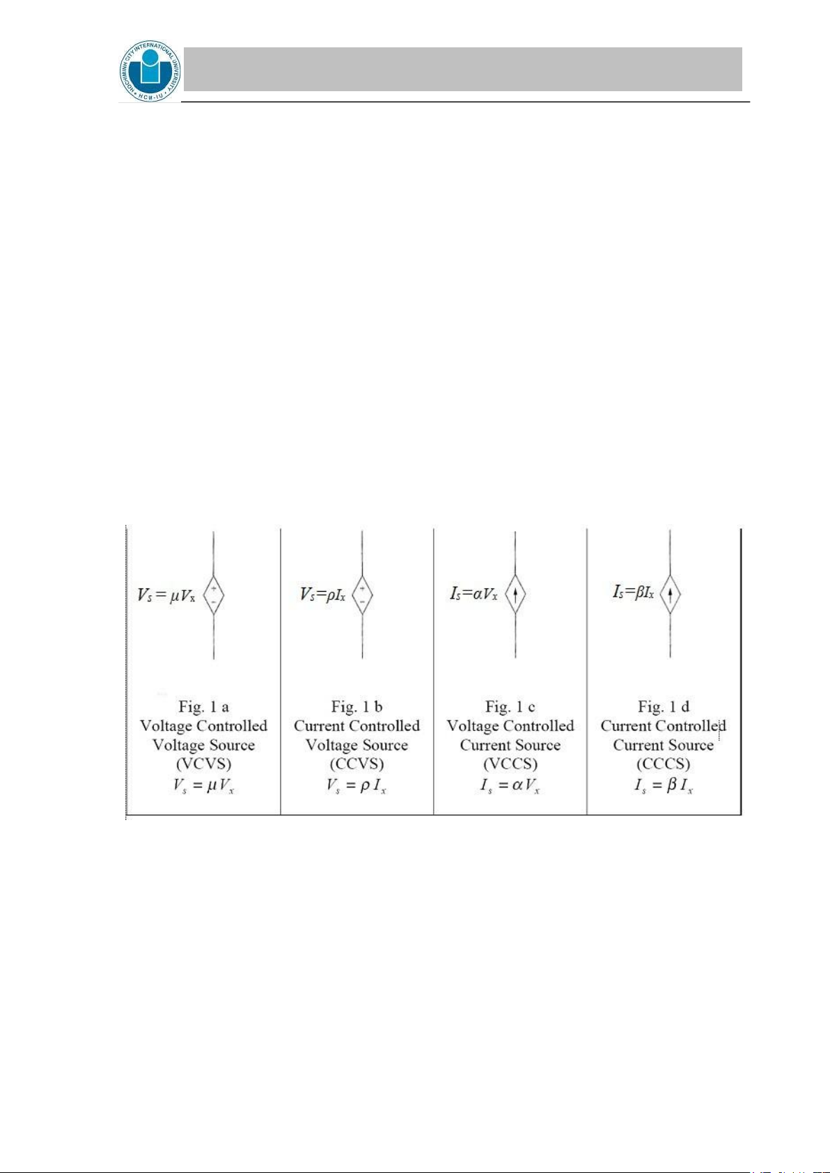
Dependent sources are sources whose value varies as a function of a specified voltage
or current elsewhere in the circuit. The relationship could be of any form, but in this course we
will introduce only those sources whose value is proportional to a voltage or current elsewhere
in the circuit. Since the output quantity can be voltage or current and so can the controlling
quantity, there are four types of such dependent sources, whose names, characteristic equations,
and symbols are shown in Fig. 1. 2.
Operational Amplifiers a. Op Amp Terminal Characteristics
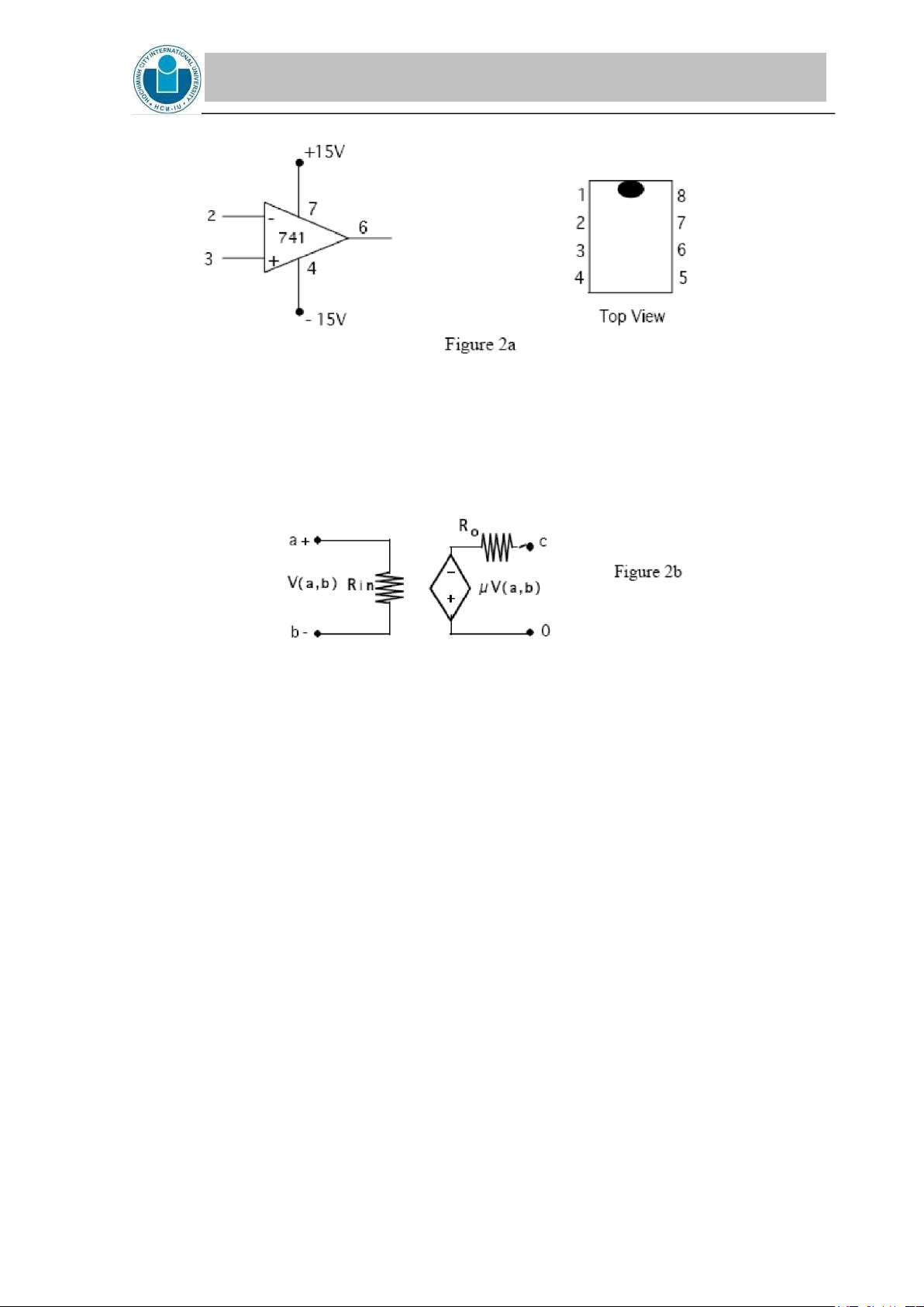
A 741 Op-Amp is shown in Fig. 2 below. Op-Amps have two input terminals; the input
voltage Vi to the Op-Amps is taken across these terminals. One terminal is called inverting or
negative and the voltage there is usually denoted as Vn and the other as noninverting (Vp) so
that Vi=(Vp-Vn). The output is taken between Vo and ground. Additional terminals (such as +Vcc,
or -Vcc) are used for bias, offset etc. lOMoAR cPSD| 58097008 INTERNATIONAL UNIVERSITY
SCHOOL OF ELECTRICAL ENGINEERING (EE)
The realistic model of an operational amplifier is given in your text and repeated below
with equivalent notation. It involves separate input and output circuits. The input consists of an
input resistance Ri between the inverting and noninverting terminals. The output consists of a
voltage dependent voltage source (with voltage AvVi) in series with an output resistance Ro.
Note that the only connection between the input and output is through the proportionality
relation of the dependent source.
The parameters involved are as follows: i.
Input Voltage Vi: V(a,b)=Vi=(Vp-Vn). ii.
Output Voltage Vo: The output voltage of an Op-Amp is proportional to the input
voltage, provided it remains less in absolute value than the DC bias voltages Vcc and -Vcc. iii.
Input Resistance Ri : The input resistance appears between the inverting and
noninverting terminal (so that Vi appears across Ri) and can be found by dividing
the input voltage Vi by the current entering the non-inverting input terminal Vp or
exiting the inverting terminal Vn. iv.
Open Loop Voltage Gain μ or Av: The open loop voltage gain is the
proportionality constant in the dependent source equation where V = AvVi (or V=μV(a,b)). v.
Output Resistance Ro: The output resistance appears as a resistor in series with
the dependent source. In the presence of a non-zero output resistance Ro, the output
voltage across a load RL is not all of V = AvVi and can be found by analyzing the
voltage divider between Ro and RL. lOMoAR cPSD| 58097008 INTERNATIONAL UNIVERSITY
SCHOOL OF ELECTRICAL ENGINEERING (EE)
b. Linear Operation and Saturation
Op-Amps have two regions of operation: linear and saturation. In the linear region, the
voltage transfer characteristic, i.e. the mathematical relationship between the input and output
voltages, is linear. This holds true when the output voltage lies in the range -Vcc ≤ V0 ≤ Vcc
From the definition of voltage gain given above, i.e. Vo = AvVi, one can see that this
range corresponds to input voltages in the range of V cc Av i Av
In this range the output voltage is directly proportional to the input voltage, by the factor Av.
For input voltages outside this range, the Op Amp is said to be saturated, and its output
is bounded by the DC bias voltages. In other words, the output voltage is clamped to -Vcc when
Vi < -Vcc/Av and to Vcc when Vi > Vcc/Av.
c. Characteristics of an Ideal Op-Amp i.
Ri = : According to the definition of input resistance given above, an infinite
input resistance means that no current flows into or out of the input terminals. This
greatly simplifies the analysis of Op-Amp circuits. ii.
Ro = 0: In this case the entire dependent source voltage appears across the load
resistance or as the input of another device. iii.
μ =AV = : If the output voltage is to be finite it follows from the definition of
voltage gain, that Vi = Vo / Av will go to zero if Av is infinite. This, however, assumes
that there is some way for the input to be affected by the output. Indeed this will
only happen if there is such a connection namely a negative feedback mechanism
in the form of a connection between the output and the inverting terminal (closed
loop operation). If such connection does not exist, then the output will be saturated
(open loop operation). For closed loop operation, it is said that a virtual short exists
between the positive and negative input terminals. This means that if an Op-Amp
is operating in its linear region (if it is unsaturated) then Vi 0, or equivalently Vp
Vn. This also simplifies the circuit calculations at the input terminals, because Vp
and Vn can be represented by a single variable. When one of
the two terminals is grounded, then the voltage at both terminals is zero and the
other terminal is called a virtual ground. lOMoAR cPSD| 58097008 INTERNATIONAL UNIVERSITY
SCHOOL OF ELECTRICAL ENGINEERING (EE)
d. Building Amplifier Circuits Using Op-Amps
There are two standard closed-loop connections for an Op-Amp. Both have in common
the connection (Rf) from the output terminal to the inverting input terminal. This connection
provides the negative feedback and ensures the virtual short. The analysis is simple for ideal Op-Amps since: i.
the two input terminals are at the same voltage and ii.
there is no current into the input terminals.
The analysis usually derives a gain or amplification. It is important to note that this is
the gain of the whole stage (or the closed loop gain) and should not be confused with the gain of the Op Amp alone.
One last note: negative feedback does not guarantee that the amplifier will not saturate.
If the input is such that the output, based on the amplification of the whole stage, is expected to
be larger than the bias voltage in absolute value (Vo> +Vcc or Vo< -Vcc) then the output will be
clamped to Vcc (or -Vcc). e.
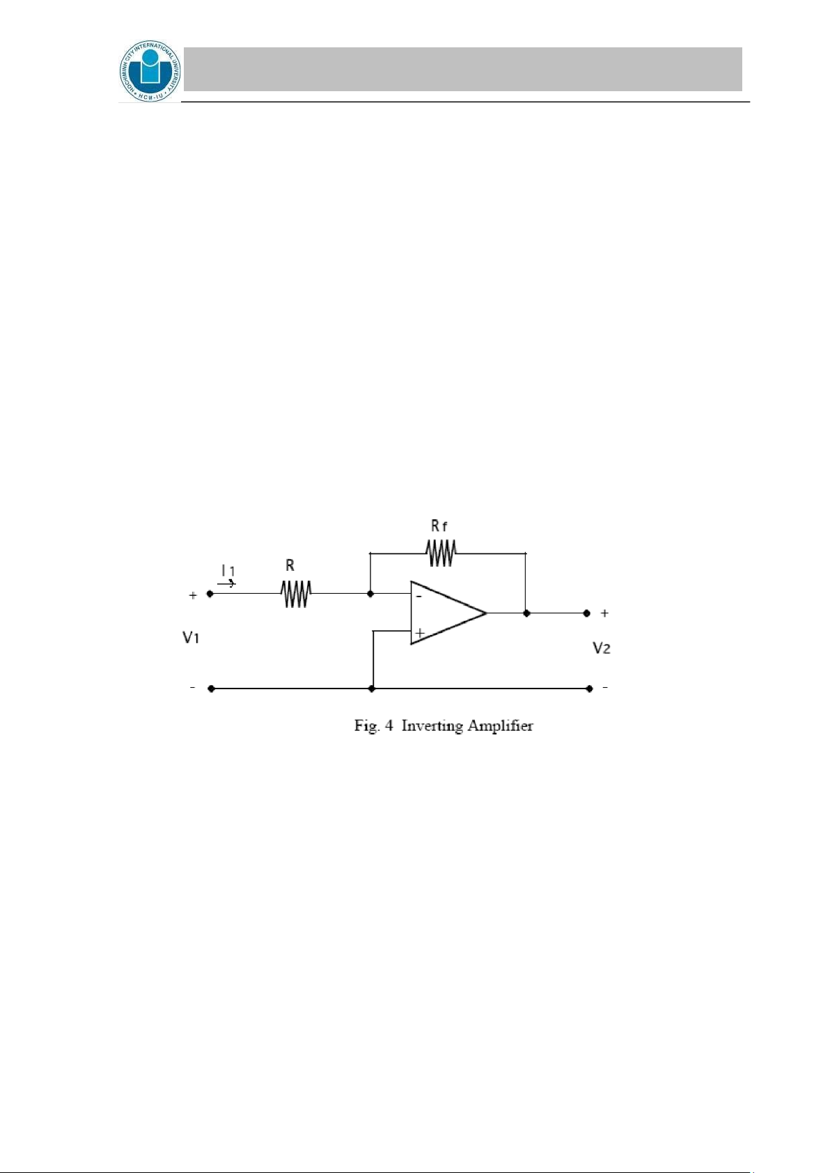
The Inverting Amplifier
Circuit analysis of the inverting amplifier in Fig. 4 yields the equation,
V2 = K V1 = (-Rf / R)V1 (1)
Thus, the theoretical gain K of the whole stage (that is, the entire Op-Amp circuit of Fig 4.) is given by K = V2/V1= (-Rf / R). f.
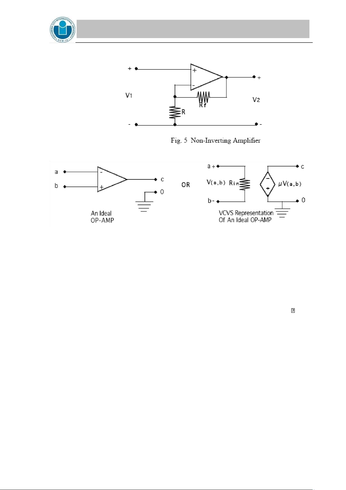
The Non-Inverting Amplifier
Circuit analysis of the non-inverting amplifier shown in Fig. 5 yields the equation, V2 = (1+Rf / R)V1 (2)
Thus, the theoretical gain K of the whole stage is given by lOMoAR cPSD| 58097008 INTERNATIONAL UNIVERSITY
SCHOOL OF ELECTRICAL ENGINEERING (EE)
K = V2/V1= (1 + Rf / R).
g. Simulating Op Amps in PSpice Figure 6
Using a VCVS, one can construct a model of the Op-Amp for use in SPICE. The circuit
of Fig. 2b can be used to model a non-ideal1 Op-Amp using two resistors and a dependent voltage source.
The circuit of Fig. 6 can be used for simulating an ideal Op Amp and is derived from
Fig. 2b by shorting out the output resistor Ro (which is equivalent to setting its value equal to
zero) and by picking large values for the input resistor Ri and for the Op-Amp voltage gain μ
(or A). Typical such values for approximating an ideal Op-Amp in PSpice are Ri=1010 and μ =106. III. PRE-LABRATORY 1. Theory i.
Briefly explain why one can assume Vp=Vn for an ideal Op-Amp. What
connection has to be present for this to occur? ii.
What is the gain of an amplifier circuit? How is it different from the Op-Amp gain? lOMoAR cPSD| 58097008 INTERNATIONAL UNIVERSITY
SCHOOL OF ELECTRICAL ENGINEERING (EE) 2. Experiment 1 i.
Calculate the gain K for the non-inverting amplifier circuit in Fig. 8 (from
section 5.1 below) assuming that the Op-Amp is ideal and using the resistance values specified in 5.1.1. ii.
Calculate the theoretical range of the input voltage for linear operation of the circuit in Section 5.1. iii.
Simulate the experimental procedure of Section 5.1 in PSpice by choosing 3
different points in the linear operating range, and calculating the circuit gain at each of these points. iv.
The PSpice Op Amp model presented in Section 3.2.5 does not account for the
effects of saturation, so this portion of the experiment cannot be simulated in
PSpice. Describe how you would expect the circuit to behave outside its range of linear operation. 3. Experiment 2 i.
Calculate the gain K for the inverting amplifier circuit of Fig. 9 (from Section
5.2 below) assuming that the Op-Amp is ideal. The answer should be in terms of R and Rf. ii.
Given the results of question 4.7, calculate the values of R and Rf that produce
a circuit gain of -4.545 and a voltage Vi=0.5V when Vs=5V. iii.
Simulate the experimental procedure from Section 5.2 in PSpice by choosing
3 different points in the linear operating range, and calculating the circuit gain at each of these points. IV.
EQUIPMENT AND PARTS LIST
• Electronic board with Power Supply • Digital Multimeter • 741 Operational Amplifier
• 10KΩ, 2.2KΩ, 15kΩ, 20kΩ, 4.7kΩ Resistors lOMoAR cPSD| 58097008 INTERNATIONAL UNIVERSITY
SCHOOL OF ELECTRICAL ENGINEERING (EE) V.
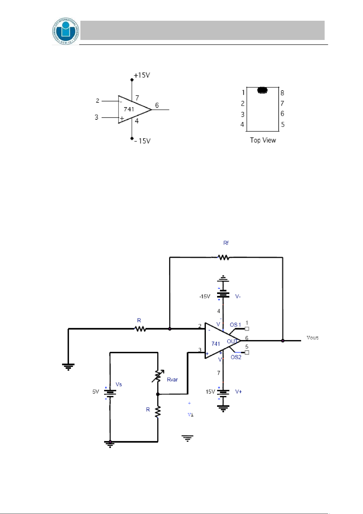
PROCEDURES Part 1. Non-Inverting Amplifier Figure 7 Op Amp 741
You will be using the "741" Op-Amp which is biased at +15V and -15V. The chip layout
is shown in Fig. 7. The standard procedure on such chip packages (DIP15) is to identify pin 1
as the one to the left of the notch in the chip package. The notch always separates pin 1 from
the last pin on the chip. In the case of 741, the notch is between pins 1 and 8. Pins 2, 3, and 6
are the inverting input Vn , the non-inverting input Vp, and the amplifier output Vo respectively.
These three pins are the only three terminals that usually appear in an Op-Amp circuit schematic diagram. lOMoAR cPSD| 58097008 INTERNATIONAL UNIVERSITY
SCHOOL OF ELECTRICAL ENGINEERING (EE) Figure 8 1.
Construct the circuit in Fig. 8 with R =2.2k , Rvar=20k and Rf =10k . 2.
Use the fixed 5V power supply of the power source for Vs. Vary Rvar’s value so that
you can change Vi. Take readings for the output voltage Vout for values of Vi from 3.5V
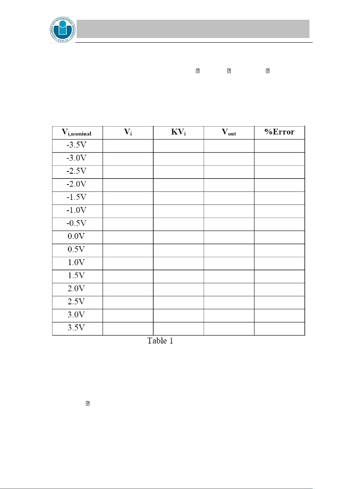
to +3.5V in increments of 0.5V and record them in Table 1. Calculate KVi for each Vi
using the calculated gain K found in prelab item 4.3 above. Calculate the % error for each row in the table. 3.
For an input voltage of your choice that keeps the Op-Amp in the linear region, place
an ammeter in series with Rf. Record the value of the current I.
Vi = ____________ . I = ______________ . 4.
Disconnect the ammeter. Keep the input voltage the same as in 5.1.3 above. Place a
10k load resistor between the output terminal of the Op-Amp and ground. In so doing
one can study the output resistance characteristics of the Op-Amp. Measure the output
voltage Vout with the DVM, and compare with the results obtained for the same input
voltage in item 5.1.2. Explain any discrepancies by assuming a nonzero Op-Amp lOMoAR cPSD| 58097008 INTERNATIONAL UNIVERSITY
SCHOOL OF ELECTRICAL ENGINEERING (EE)
output resistance. Later you will be asked to calculate the output resistance of the Op Amp based on these results. lOMoAR cPSD| 58097008 INTERNATIONAL UNIVERSITY
SCHOOL OF ELECTRICAL ENGINEERING (EE)
Vi = _____________. Vout = ____________. K = ______________. 5.
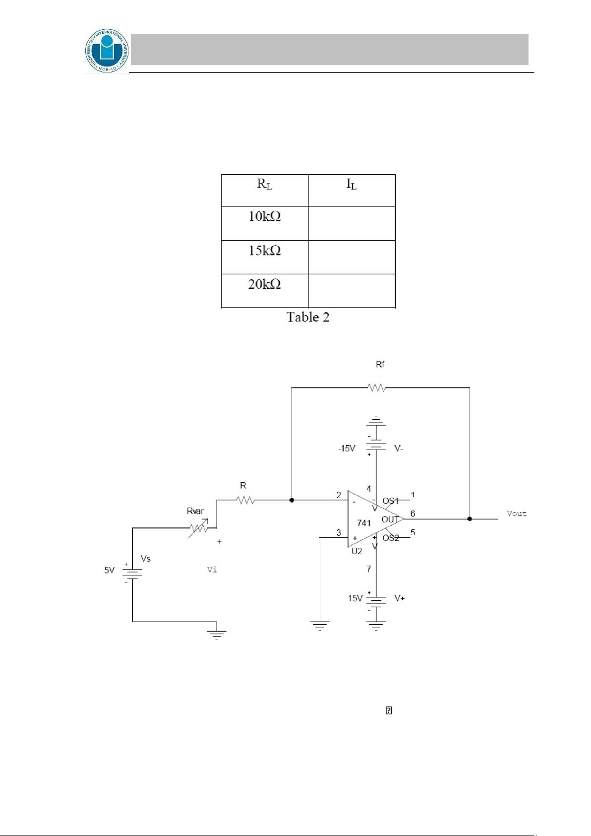
This item involves the study of the relationship between the load resistance and output
voltage (and thus also voltage gain). Keeping the source voltage at 5V, measure IL
(the current through the load resistance RL) for each value of RL in Table 2. Later, you
will be asked to analyze this data.
Part 2: Inverting Amplifier Figure 9
1. In prelab item 4.7 you should have calculated the values of Rf and R that yield a circuit
gain of -4.545 and Vi=.5V when Vs=5V and Rvar=20k . Get your TA to check your
calculations and correct them if necessary, then build the circuit of Fig. 9 with the correct values of Rf and R. lOMoAR cPSD| 58097008 INTERNATIONAL UNIVERSITY
SCHOOL OF ELECTRICAL ENGINEERING (EE)
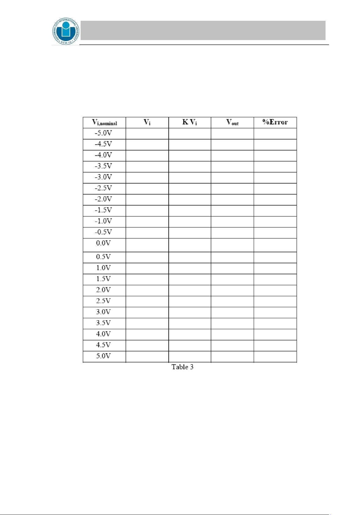
2. Use the fixed 5V power supply of the power source for Vs. Vary Rvar’s value so that you
can change Vi. Take 21 readings for the output voltage Vout at each value of Vi from -5V
in increments of 0.5V and record them in Table 3. Calculate KVi for each Vi in Table 3
using the calculated gain K found in prelab item 4.7 above. Calculate the % error for
each row in the table. If the measured Vout differs from KVi by more than 10% you
probably have an error in the circuit. Troubleshoot the circuit until it is operating properly. VI. REPORT
1. Derive the relationship between the current I and the resistor Rf in the non-inverter circuit of Fig. 8.
2. Compare the theoretical value of the gain K = Vout /Vi of both the inverting and the
non-inverting circuits of Sections 5.1 and 5.2 that you calculated in the prelab exercises
with the experimentally obtained values of gain. lOMoAR cPSD| 58097008 INTERNATIONAL UNIVERSITY
SCHOOL OF ELECTRICAL ENGINEERING (EE)
3. Calculate the theoretical value of the current I for the resistor Rf in Section 5.1. Compare with the experimental one.
4. Calculate the theoretical values of the current IL for all three values of RL in Section
5.1.5. Compare with the experimental ones.
5. Plot the experimental values of IL vs. 1/RL in a graph with rectangular coordinates. From
your graph, how does your output voltage depend on the load? How does the gain K=
Vout /Vi depend on the load? Note that if Vout does not change with the load RL, and since
IL = Vout (1/RL), then the slope is Vout and it should be constant and thus the graph of IL
vs. 1/RL should be a straight line passing through the origin.
6. Draw two graphs of the experimentally obtained Vi vs. Vout, one for the inverting
amplifier circuit and one for the non-inverting amplifier circuit (5.1 and 5.2). On each
graph identify the transition between saturated and linear regions of operation for these
amplifier circuits. Label the mode of operation for each of these regions. For the linear
regions and for both circuits, discuss the possible sources of discrepancies between the
experimentally obtained value of Vout and the calculated values of KVi.
7. Simulate the non-inverter circuit of Fig. 8 in PSpice for Rf = 10k , Rvar=20 k and
R=2.2 k . Find the output voltage Vout and the current I in Rf. Assume a μA741 Op Amp.
8. Simulate the non-inverter circuit of Fig. 8 in PSpice for Rf = 10k with a load RL =
10k applied between the output terminal of the Op-Amp and ground. Find the current in RL.
9. Simulate the inverter circuit in Fig. 9 in PSpice for Rf = 10k , Rvar=20k and R=2.2
k . Find the output voltage Vout and the current in Rf.
Tài liệu liên quan:
-
Lab 6: Mesh & Nodal Analysis of AC Circuits | Môn Principles of EE 1 - Trường Đại học Quốc tế, Đại học Quốc gia Thành phố Hồ Chí Minh
131 66 -
Lab 2: Kirchhoff's Current and Voltage Laws | Môn Principles of EE 1 - Trường Đại học Quốc tế, Đại học Quốc gia Thành phố Hồ Chí Minh
125 63 -
Lab 7: Operational Amplifiers Study Guide | Môn Principles of EE 1 - Trường Đại học Quốc tế, Đại học Quốc gia Thành phố Hồ Chí Minh
98 49 -
Review Exercises on Laplace Transform & Filter Concepts | Môn Principles of EE 1 - Trường Đại học Quốc tế, Đại học Quốc gia Thành phố Hồ Chí Minh
114 57