Lab 7: Operational Amplifiers Study Guide | Môn Principles of EE 1 - Trường Đại học Quốc tế, Đại học Quốc gia Thành phố Hồ Chí Minh
Lab 7: Operational Amplifiers Study Guide Môn Principles of EE 1. Tài liệu được sưu tầm gồm 15 trang, giúp bạn ôn tập tốt hơn. Mời các bạn đón xem.
Môn: Principles of EE 1 10 tài liệu
Trường: Trường Đại học Quốc tế, Đại học Quốc gia Thành phố Hồ Chí Minh 2 K tài liệu
Tác giả:


Preview text:
lOMoAR cPSD| 58097008
Vietnam National Universities – HCMC International University
School of Biomedical Engineering
Department of Medical Instrumentations
Principles of EE I Laboratory BM054IU Lab 7
Operational Amplifier (Op-Amp) Instructor:
Assoc. Prof. Pham Thi Thu Hien Submitted by: Full name Student ID Contribution Ho Chi Minh City
Semester 2, 2023 - 2024 1. Pre-lab
*You must provide all calculations in-details in separate sheets and/or simulation results as attachments. lOMoAR cPSD| 58097008
Vietnam National Universities – HCMC International University
School of Biomedical Engineering
Department of Medical Instrumentations Theory:
Question 1. Briefly explain why we assume V+ = V- for an ideal op-amp. What
connection must be present for this to occur?
Question 2. What is the gain of a negative-feedback amplifier circuit? How is it
different from the open loop gain of op-amp?
Question 3. Why would you ever want to use the follower/buffer amplifier circuit? Experiment 1:
Question 4. Calculate the theoretical gain Ar of the inverting amplifier circuit in Fig.8
assuming that the op-amp is ideal. Your answer should be in terms of R and Rf and filled in Table 1.
Question 5. Calculate the theoretical voltage gain and output voltage in Table 2.
Question 6. Calculate the theoretical output voltage in Table 3. Experiment 2:
Question 7. Calculate the theoretical output voltage of the non-inverting amplifier circuit in Table 4 Experiment 3:
Question 8. Calculate the theoretical output voltage and the gain of the follower/buffer
op-amp in Fig.10 and fill it in Table 5. 2. Lab objectives
This lab studies the characteristics of the operational amplifiers and several simple circuits
understanding of how op-amps are used.
• Introduction to op-amps, linear and saturation region, and characteristics of ideal opamps.
• Voltage amplifiers (inverting and non-inverting). • Follow/Buffer amplifier. 3. Background information 3.1. Op-amp
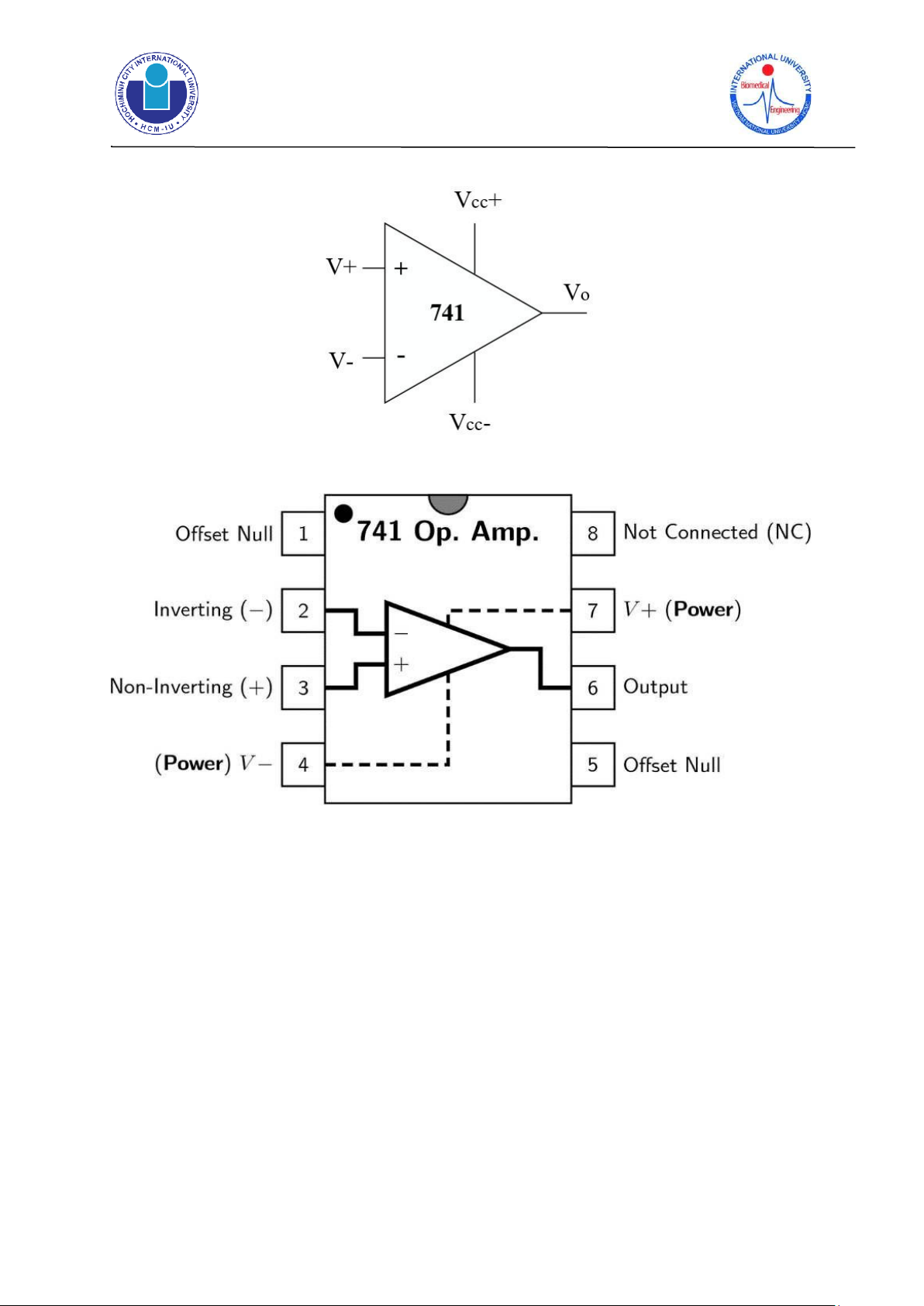
The operational amplifier named IC 741 is used in this lab involving linear
amplification. The most fundamental op-amp symbol has five terminals: two supply terminals
(Vcc+ and Vcc-), two inputs (V+ is a positive or non-inverting input, V- is a negative or
inverting input), and one output Vo. lOMoAR cPSD| 58097008
Vietnam National Universities – HCMC International University
School of Biomedical Engineering
Department of Medical Instrumentations
Fig. 1. The op-amp symbol Fig. 2. IC 741 pin out
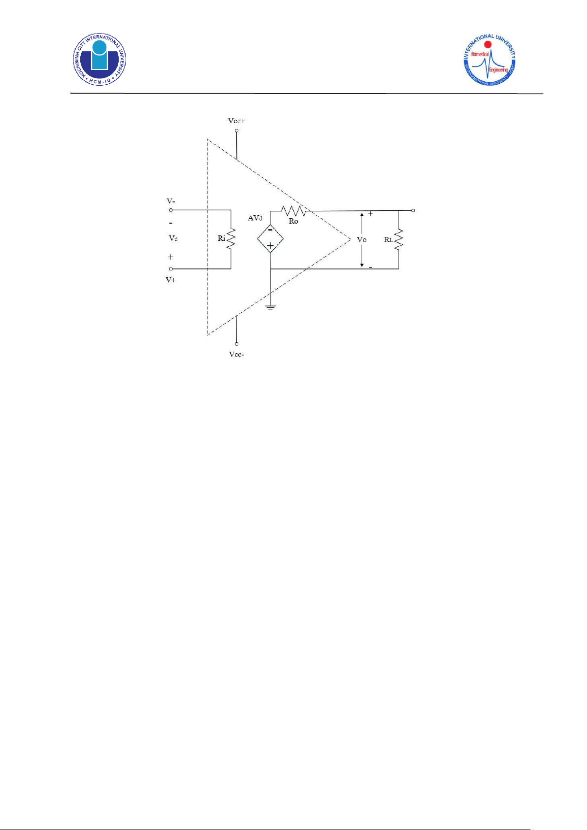
In Fig. 3 below, the circuit is referred to as an "equivalent circuit of an op-amp" as it
depicts op-amp parameters in terms of physical components for analytical purposes. The output
part is defined as a voltage-controlled dependent voltage source in series with the output
resistance Ro. The output resistance Ro is the Thevenin equivalent resistance seen at the output
terminal. The input resistance Ri is the Thevenin equivalent resistance seen at the input terminals. lOMoAR cPSD| 58097008
Vietnam National Universities – HCMC International University
School of Biomedical Engineering
Department of Medical Instrumentations
Fig. 3. The Equivalent Circuit of Practical Op-Amp
In the absence of any load at the output, according to the op amp’s equivalent circuit
described above, the op amp detects the difference between the two inputs, multiplies it by gain
A, and then causes the resultant voltage to appear at the output.
Vo = AVd = A(V+ – V-) Where:
A: Large signal open loop voltage gain since it is the gain of the op amp without any
external feedback from output to input.
Vd: Difference voltage V+ – V-
V+: Noninverting input voltage with respect to ground V-:
Inverting input voltage with respect to ground
Ri: Input resistance of op-amp
Ro: Output resistance of op-amp
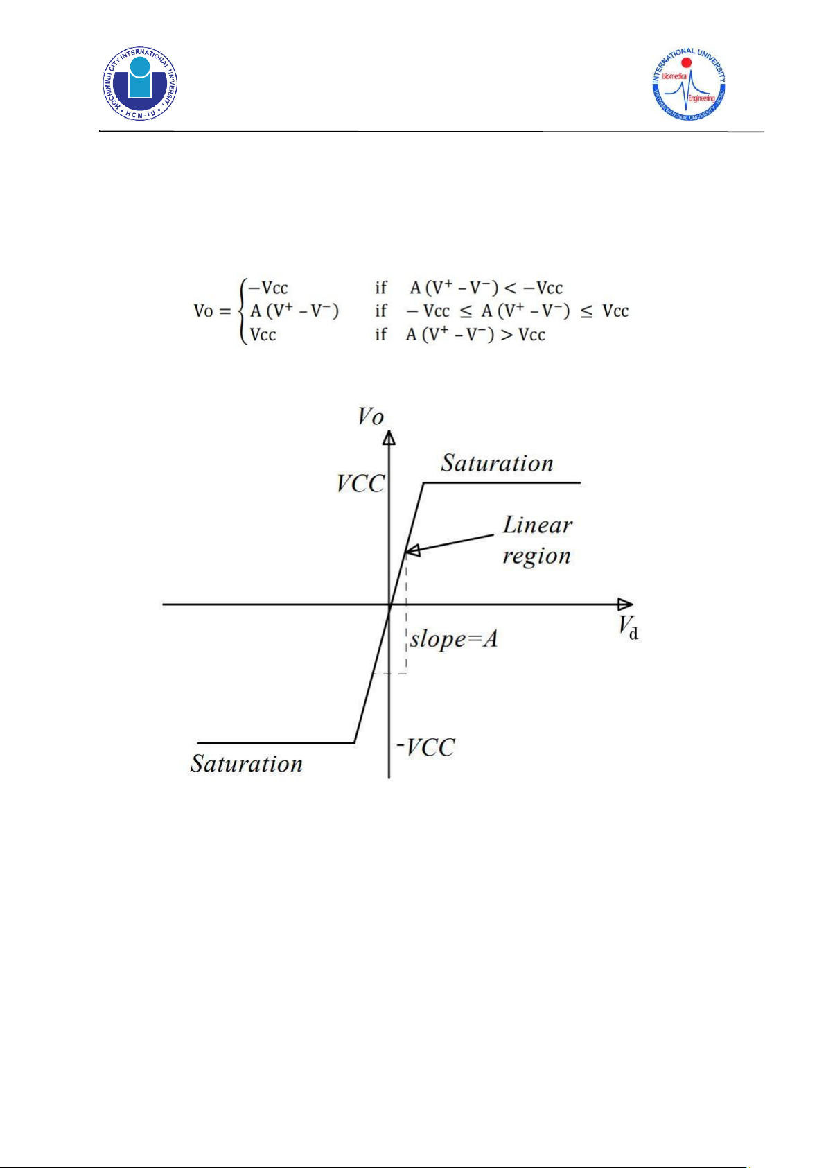
3.1.1. Linear and Saturation Region
An op-amp can only output voltages that fall within the range of its power source. The
op-amp is said to saturate when the output voltage of the circuit would exceed the permissible
range, and it simply produces its maximum or lowest value instead. The rails are a common
name for the supply voltages. When op-amp output saturation results in a signal cutoff that is
relatively close to the rails, we refer to the signal as clipped. The output voltage cannot be more
than |Vcc| in magnitude. Op-amps can function in one of three modes depending on the power
supply voltage and the differential input voltage Vd: lOMoAR cPSD| 58097008
Vietnam National Universities – HCMC International University
School of Biomedical Engineering
Department of Medical Instrumentations
• Positive saturation: Vo = Vcc
• Linear region: -Vcc ≤ Vo ≤ Vcc
• Negative saturation: Vo = -Vcc
The voltage transfer characteristics combine the three regions of mode.
The graph that relates the output voltage to the input voltage is called the voltage transfer curve
and is fundamental in designing and understanding amplifier circuits.
Fig. 4. The voltage transfer curve of op-amp
3.1.2. Characteristics of ideal op-amp
An op amp is ideal if it has the following characteristics:
• Infinite open-loop gain, i.e., A = ∞
• Infinite input resistance, i.e., Ri = ∞ Ω
• Zero output resistance, i.e., Ro = 0 Ω
Two important characteristics of the ideal op amp for circuit analysis: lOMoAR cPSD| 58097008
Vietnam National Universities – HCMC International University
School of Biomedical Engineering
Department of Medical Instrumentations
• The current into both input terminals is zero, i.e., i+ = i- = 0. This is due to infinite
input resistance: an open circuit exists between two terminals and current cannot flow through.
• The voltage across the input terminals is negligibly small, i.e., v = v-. This is due to infinite open-loop gain.
3.2. Voltage Amplifiers
The op-amp circuit is configured with negative feedback in this lab. In other words, a
part of the input is negated when the output is connected back to the input. At the cost of
decreasing the gain, negative feedback increases the amplifier’s linearity, frequency
responsiveness, noise performance, and stability. With negative feedback, the characteristics of
the amplifier circuit depend on the feedback network’s characteristics rather than the op amp’s
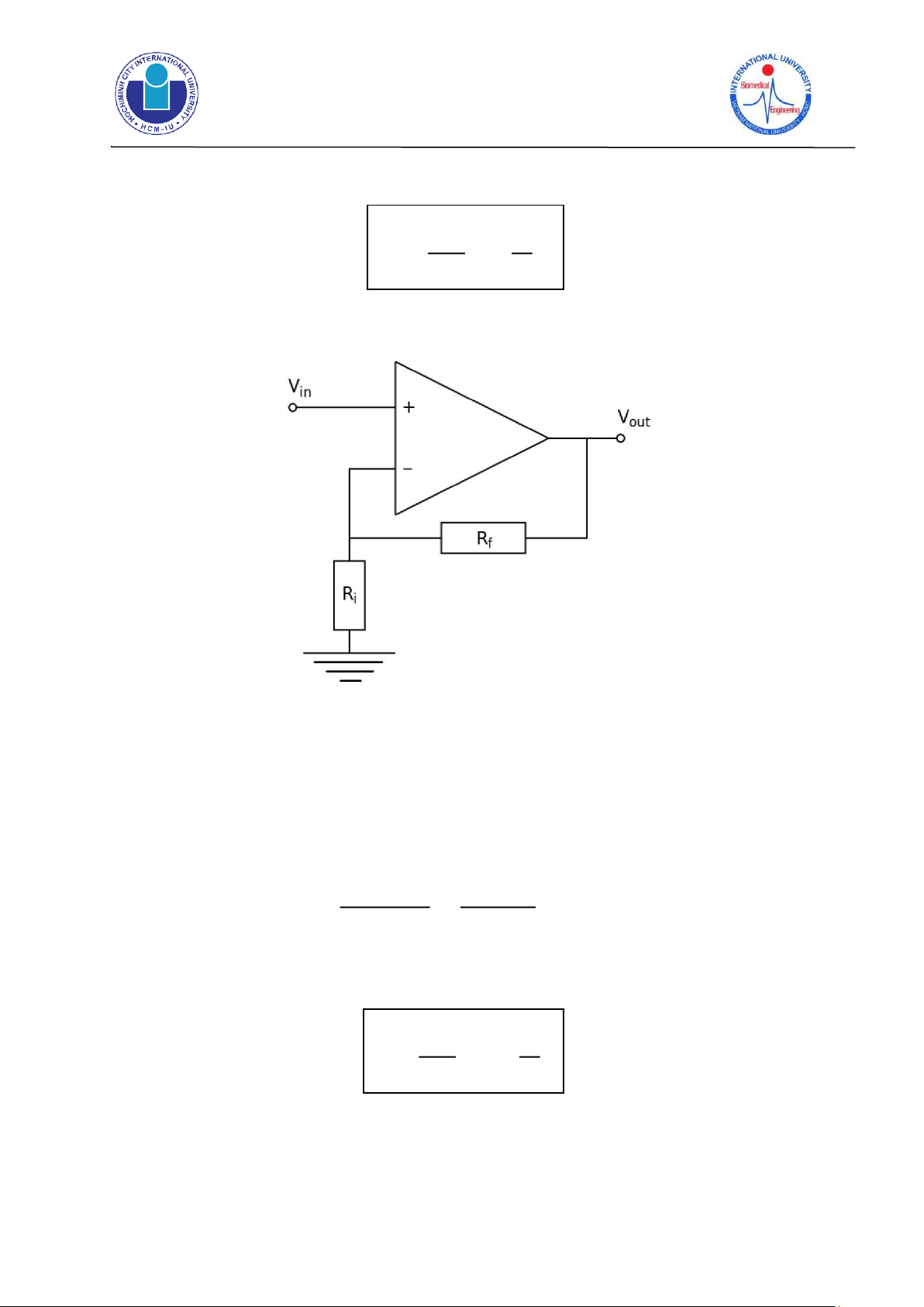
open-loop characteristics. 3.2.1. Inverting Amplifier
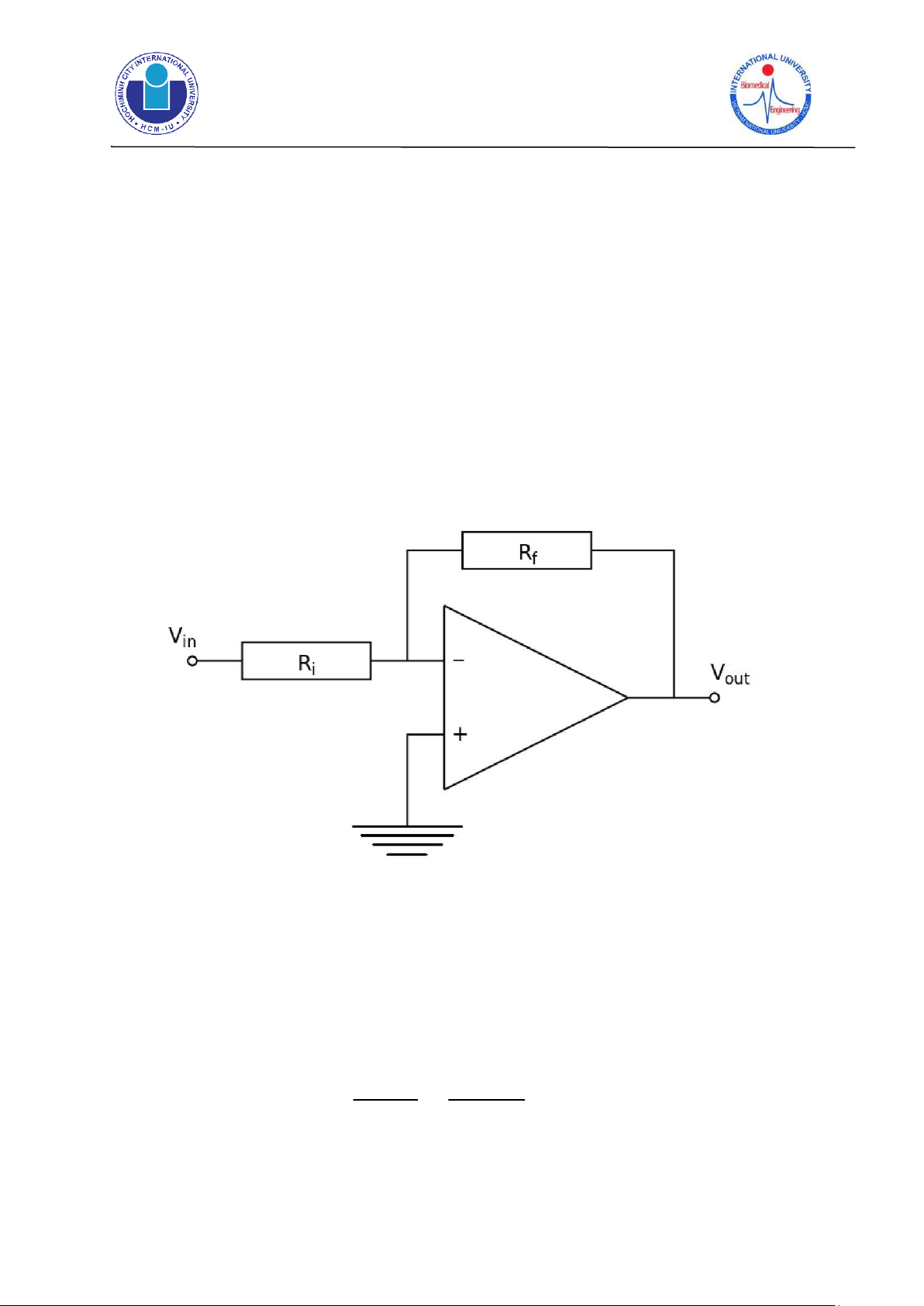
Fig. 5. The inverting amplifier
An inverting operational amplifier (or op-amp) is used to generate an output signal that
is 180 degrees out of phase with the applied input signal. With an inverting amplifier, if the
input signal has positive phase, the amplified output signal will have negative phase, and vice
versa. Once this amplifier is assumed as an ideal, we apply the virtual short notion at the opinput
amp’s terminals. As a result, the voltage at the two terminals is equal. The Kirchhoff current
law (KCL)should be used at the amplifier circuit’s inverting node. 0 − Vin 0 − V𝑜𝑢𝑡 + = 0 Ri Rf
By simplifying the above terms, we will get the following formula. lOMoAR cPSD| 58097008
Vietnam National Universities – HCMC International University
School of Biomedical Engineering
Department of Medical Instrumentations
The gain of the inverting amplifier is: Vout Rf Av = = − Vin Ri
3.2.2. Non-inverting Amplifier
Fig. 6. The non-inverting amplifier
In this kind of amplifier, the output is exactly in phase to input. If the input signal has a
positive phase, the amplified output signal will likewise have a positive phase, and vice versa
for negative phase. Once this amplifier is assumed as an ideal, we apply the virtual short notion
at the op-input amp's terminals. So, the voltage at the two terminals is equivalent to each other.
Apply KCL at the inverting node in the circuit: Vin − Vout Vout − 0 + = 0 Rf Ri
By modifying the above terms, we can get the following formula.
The gain of the non-inverting amplifier is: Vout Rf Av = = 1 + Vin Ri lOMoAR cPSD| 58097008
Vietnam National Universities – HCMC International University
School of Biomedical Engineering
Department of Medical Instrumentations
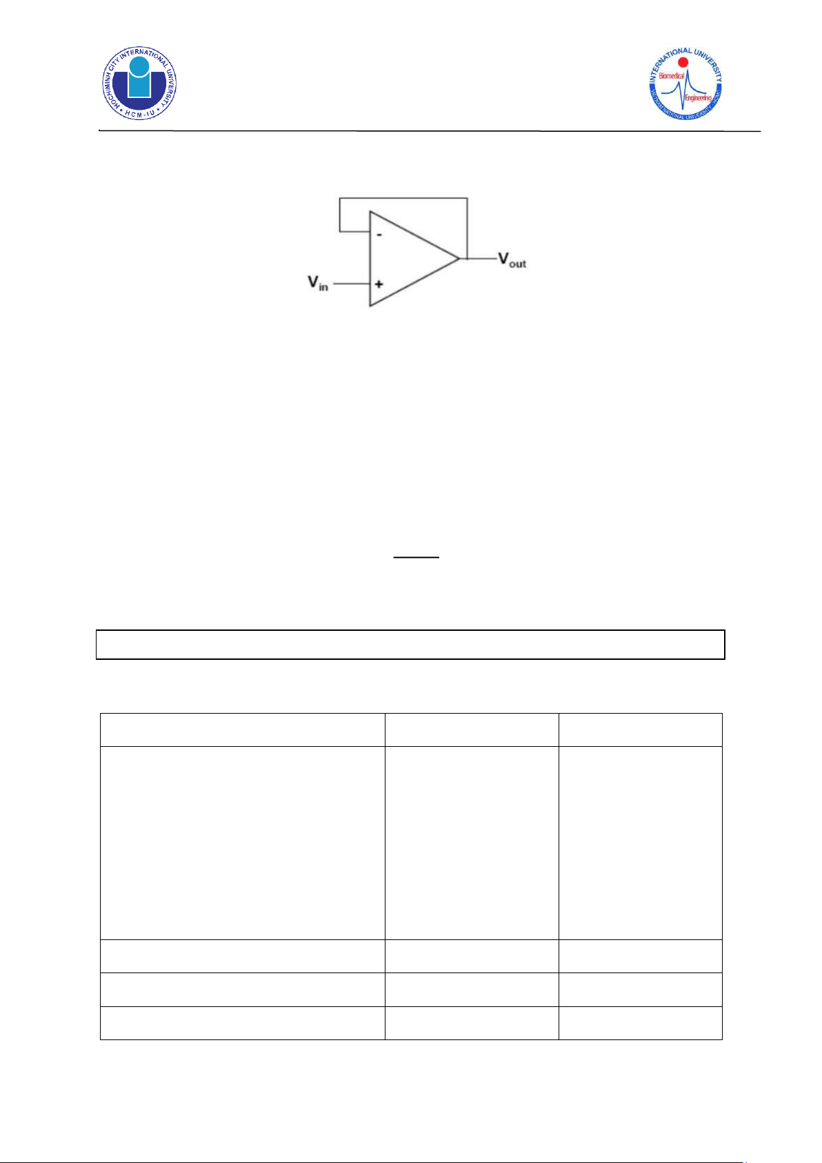
3.3. Follow/Buffer Amplifier
Fig. 7. The follow/buffer amplifier
A voltage follower is an op-amp circuit whose output voltage is identical to the input
voltage (it "follows" the input voltage), also known as a buffer amplifier, unity-gain amplifier,
or isolation amplifier. Consequently, a voltage follower op-amp has a voltage gain of 1 and
does not increase the input signal. In the Fig.7, it shows the inverting input is tied to the output
V− = Vo, and the non-inverting input is tied to the input voltage V+ = Vin.
Vo = A (V+ - V−) = A (Vin - Vo) A VO = Vin A + 1
With the open-loop gain is extremely large; the output voltage becomes: Vo = Vin
4. Materials and equipment Name Value Number Resistors 1 kΩ 2 10 kΩ 2 20 kΩ 1 33 kΩ 1 47 kΩ 1 68 kΩ 1 100 kΩ 1 Operational Amplifier µA 741 - 1 Digital Multimeter (DMM) - 1 Oscilloscope - 1 lOMoAR cPSD| 58097008
Vietnam National Universities – HCMC International University
School of Biomedical Engineering
Department of Medical Instrumentations Function Generator (AC Power - 1 Supply) DC Power Supply - 1 DMM Probes - 2 Oscilloscope Probes - 2 Protoboard - 1 Wire 22 AWG x 6nos. - 6
5. Safety precautions (in case of any possible lab hazards).
(1) Make sure that the power has been switched off safely after using electrical equipment.
(2) If the power cannot be switched off, operate the device with just one hand. This will stop a
circuit from entering your heart, which might be fatal.
(3) Internal energy storage systems, such as capacitors, must be discharged.
(4) When handling high voltage, put on insulating gloves made of leather, strong cotton, or rubber.
(5) When dealing with electrical devices, only use tools and equipment with non-conducting handles.
(6) Never make wire changes while the circuit is connected to a power source.
(7) Never plug leads into power source unless they are connected to an established circuit.
(8) Avoid using moist hands or other wet objects to interact with circuits.
(9) Verify that circuits are properly grounded in relation to the power source.
(10) Avoid using extremely flammable substances close to electrical equipment.
(11) Before turning on the power, double check circuits for good connections and polarity. When
wiring components into a circuit, especially electrolytic capacitors, always observe polarity.
(12) Before conducting a measurement, double-check that the test instruments are set for the correct function and range. lOMoAR cPSD| 58097008
Vietnam National Universities – HCMC International University
School of Biomedical Engineering
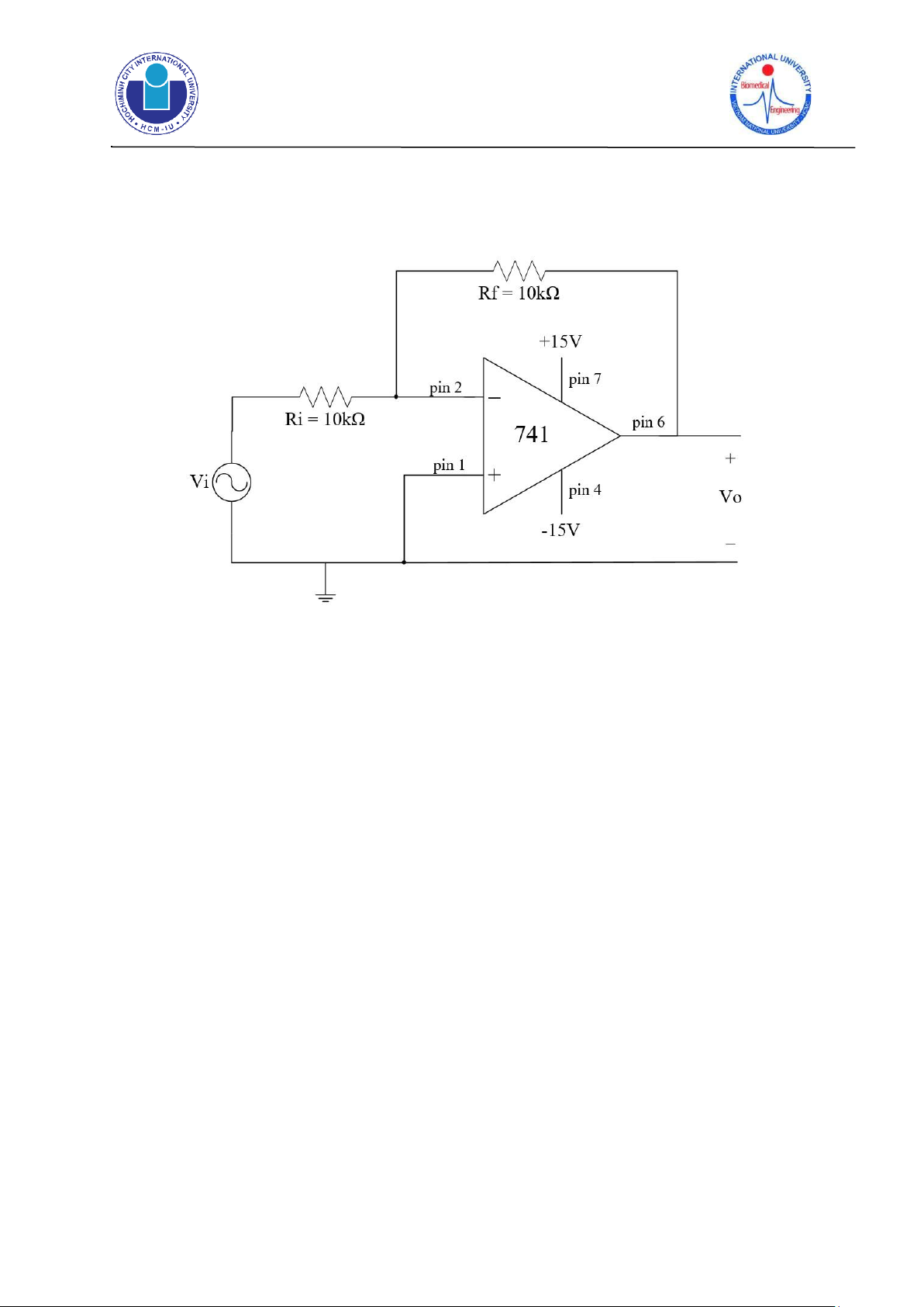
Department of Medical Instrumentations 6. Experimental procedure 6.1. Inverting Amplifier
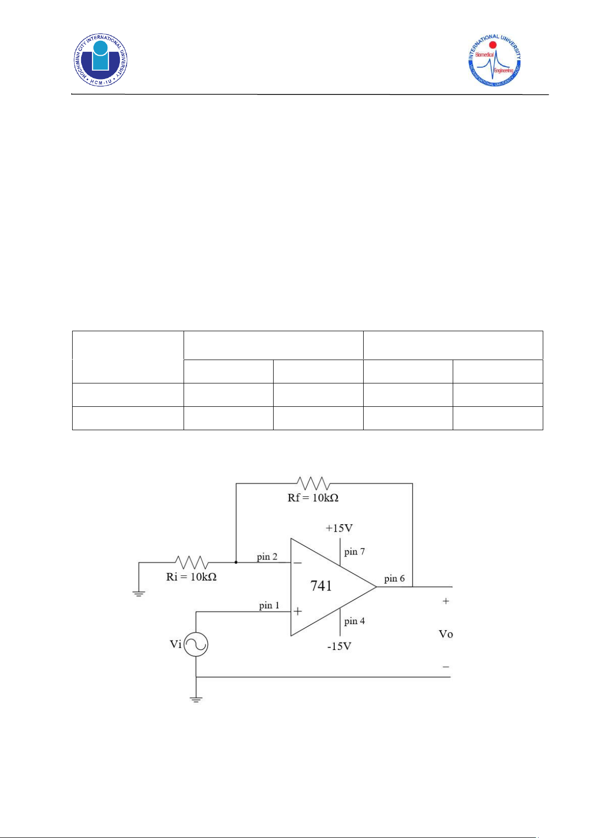
Fig. 8. The experimental inverting amplifier
Step 1: Connect circuit diagram according to given circuit shown in Fig.8. The DC power
supply is used to provide voltages at +15V and -15V with respect to ground for two power
supply inputs of the op-amp. DMM (Digital Multimeter) is used for evaluating DC supply accuracy.
Step 2: Use the function generator to apply sine wave input signal using f=500Hz with amplitude of 4Vp-p.
Step 3: Connect the oscilloscope to the input and output voltage of the circuit to display the
Vin and Vout waveforms. Measure the peak-to-peak amplitude of the output signal (Vo p-p)
using oscilloscope, compare to input signal and calculate the voltage gain Av.
Step 4: Vary the feedback resistor value, Rf
• Use DMM to measure the actual value of Rf = 20kΩ, 33kΩ, 47kΩ, 68kΩ and 100kΩ with Ri=10kΩ.
• The theoretical gain, AR is compared to measured gain, Av using the formula
- (Rf /Ri) = Vo/Vi and the readings are tabulated in Table 1.
• Calculate the percentage errors with
Nominal value − Measured value %Error = | | × 100% lOMoAR cPSD| 58097008
Vietnam National Universities – HCMC International University
School of Biomedical Engineering
Department of Medical Instrumentations Nominal value Rf (Ω) Vi(V) Vo(V)
Ar = Rf/Ri Av = Vo/Vi % Error
Nominal Measured Nominal Measured Measured Theoretical Measured
Table 1. Variable Feedback Resistor Results
Step 5: Vary the input voltage, Vi:
• Keep the same circuit in the Fig.8 and only change Rf from 10kΩ to 68kΩ.
• The input sine wave is set at a frequency of 1 kHz. The value for peak-to peak output
voltage (Vo p-p) is measured for peak-to-peak input voltage (Vi p-p) of 1V, 2V, 4V, 6V
and 8V respectively. The readings are tabulated in Table 2.
• Calculate the measured gain for each input. Vi p-p (V) Vo p-p (V) Av = Vo/Vi Nominal Measured Theoretical Measured Theoretical Measured lOMoAR cPSD| 58097008
Vietnam National Universities – HCMC International University
School of Biomedical Engineering
Department of Medical Instrumentations
Table 2. Variable Input Voltage Results Step
6: Vary the bias voltages:
• Keep the same circuit in the Fig.8 and only change Rf from 10kΩ to 68kΩ.
• The input sine wave has a frequency of 1 kHz, and the amplitude was gradually
increased from 0V to a point where the output voltage (Vo) was clipped, or distorted,
on either the positive or negative cycle. Note the Bias voltage where the Vo is clipped.
• The peak-to-peak input and output voltages at the moment of clipping are recorded in Table 3.
• The bias voltages of pin 7 and pin 4 are reduced from +15V and -15V to +12V and -12V respectively. Bias voltage (V) Vi p-p (V) Vo p-p (V) Nominal Measured Theoretical Measured
Table 3. Variable Bias Voltage Results
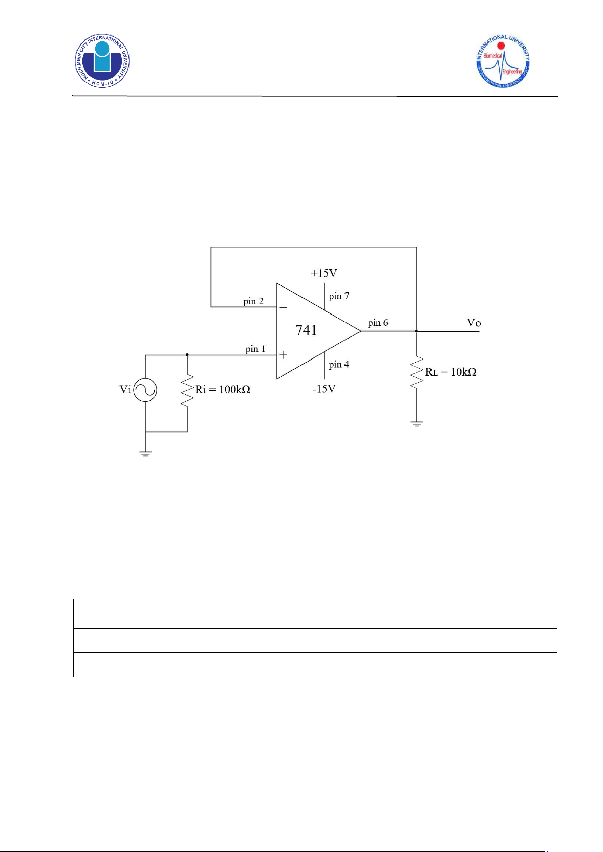
6.2. Non-inverting Amplifier
Fig. 9. The experimental non-inverting amplifier lOMoAR cPSD| 58097008
Vietnam National Universities – HCMC International University
School of Biomedical Engineering
Department of Medical Instrumentations
Step 1: Connect circuit diagram according to given circuit shown in Fig.9. The DC power
supply is used to provide voltages at +15V and -15V with respect to ground for two power
supply inputs of the op-amp. DMM is used for evaluating DC supply accuracy.
Step 2: Use the function generator to apply sine wave input signal using f=1kHz with amplitude of 1Vp-p.
Step 3: The value for output voltage when the peak-to-peak input voltage is set to 1V, 2V, 3V,
4V, and 5V respectively is measured. The readings are tabulated in Table 4. The measured Vo
p-p is compared to the theoretical values, which are calculated by using the measured values of resistors and measured Vi. Vi p-p (V) % Error Vo p-p (V) Nominal Measured Theoretical Measured
Table 4. Results to Verify Output Relationship
Step 4: Keep the input voltage at 5V and place a load resistor RL = 10kΩ between the output
terminal of the op-amp and ground. Measure the output voltage Vo with DMM compare with
the results obtained for the same input voltage in the step 3. Explain any discrepancies by
assuming a non-zero op-amp output resistance. Calculate the output resistance of op-amp based on the result. Answer: lOMoAR cPSD| 58097008
Vietnam National Universities – HCMC International University
School of Biomedical Engineering
Department of Medical Instrumentations
6.3. Follower/ Buffer Amplifier
Fig. 10. The experimental follower/buffer amplifier
Step 1: Connect circuit diagram according to given circuit shown in Figure 10.
Step 2: Apply sine wave input signal Vi using f=1kHz with amplitude of 2Vp-p.
Step 3: Record and compare waveform of input and output signal.
Step 4: Measure the output signal Vo using oscilloscope.
Step 5: Calculate voltage gain Av. Vo (V) Av = Vo/ Vi Theoretical Measured Theoretical Measured
Table 5. Output voltage and gain results of the follower/buffer amplifier.
Record of waveform in step 4: lOMoAR cPSD| 58097008
Vietnam National Universities – HCMC International University
School of Biomedical Engineering
Department of Medical Instrumentations 7. Assignment/ Lab report
Question 1. Compare the theoretical gain of the inverting amplifier circuit in Table 1 that you
calculated in the prelab exercises with the experimentally obtained values gain when we change
the value of the feedback resistance.
Question 2. Compare the theoretical output voltage and voltage gain in Table 2 that you
calculated in the prelab exercises with the experimentally obtained values when we change the value of the input voltage.
Question 3. Compare the theoretical output voltage in Table 3 that you calculated in the prelab
exercises with the experimentally obtained values when we change the value of the bias voltage.
Question 4. Compare the theoretical output voltage of the non-inverting amplifier circuit in
Table 4 that you calculated in the prelab exercises with the experimentally obtained values.
Question 5. Calculate the output resistance of op-amp in step 4 of section 5.2.
Question 6. Compare the theoretical output voltage and voltage gain of the follower/buffer
amplifier circuit in Table 5 that you calculated in the prelab exercises with the experimentally obtained values. 8. Clean-up
Each group is responsible for their Lab bench. After the Lab exercise is over, all equipment
should be powered down and all probes, cords, etc. returned to their proper position. Do not
cut and drop wires on the Lab bench. Lose cut wires have caused many short circuits. Your Lab
grade will be affected if your bench is not tidy when you leave the Lab. 9. Manual information
This manual is developed by:
• Assoc. Prof. Pham Thi Thu Hien, Instructor.
• M.S. Nguyen Le Y, Lab Technician.
Last updated: Semester 1, 2023-2024
Tài liệu liên quan:
-
Lab 6: Mesh & Nodal Analysis of AC Circuits | Môn Principles of EE 1 - Trường Đại học Quốc tế, Đại học Quốc gia Thành phố Hồ Chí Minh
131 66 -
Lab 4 - Exploring Operational Amplifiers and Their Configurations | Môn Principles of EE 1 - Trường Đại học Quốc tế, Đại học Quốc gia Thành phố Hồ Chí Minh
109 55 -
Lab 2: Kirchhoff's Current and Voltage Laws | Môn Principles of EE 1 - Trường Đại học Quốc tế, Đại học Quốc gia Thành phố Hồ Chí Minh
125 63 -
Review Exercises on Laplace Transform & Filter Concepts | Môn Principles of EE 1 - Trường Đại học Quốc tế, Đại học Quốc gia Thành phố Hồ Chí Minh
115 58