Tài liệu về A design of WCDMA RF transceiver with its performance measuring môn Thu phát vô tuyến | Học viện Công Nghệ Bưu Chính Viễn Thông
Wide-band code division multiple access (WCDMA) was designed to be a high performance system able to support advanced interactive applications or multiple simultaneous services with different quality of service parameters and high data rate, such as mobile commerce, position based services, and multimedia services. Tài liệu được sưu tầm, biên soạn dưới dạng file PDF gồm 4 trang, giúp các bạn học tốt, ôn tập hiệu quả, đạt kết quả cao trong các bài thi, bài kiểm tra sắp tới. Mời bạn đón xem!
Môn: Thu phát vô tuyến (TEL1416) 10 tài liệu
Trường: Học viện Công Nghệ Bưu Chính Viễn Thông 1.8 K tài liệu
Tác giả:


Preview text:
lOMoAR cPSD| 58977565 198
JOURNAL OF ELECTRONIC SCIENCE AND TECHNOLOGY OF CHINA, VOL. 5, NO. 3, SEPTEMBER 2007
A Design of WCDMA RF Transceiver with Its Performance Measuring
Jing-Fu Bao and Zhu-Sheng Kang
Abstract⎯A 2-GHz radio frequency transceiver is
The authors are with School of Electronic Engineering, University of
Electronic Science and Technology of China (UESTC), Chengdu, 610054,
presented and implemented for third generation mobile
China (e-mail: baojingfu@uestc.edu.cn).
communications using wide-band code division multiple
the commercial development of 3G mobile handsets, the radio
access (WCDMA) scheme. Performance measuring
frequency (RF) transceiver of excellent characteristics and high
systems are introduced for transmitter channel and
sensitivity has considerably received attention. Some radio
receiver sensitivity, respectively. The transceiver achieves
transceiver architectures for wideband cellular systems have
maximum output power of 22 dBm, dynamic range of 85
been widely discussed[2]. RF single-chip integration has been
dB, adjacent channel power rejection ratio (ACPR) of
recently explored for compatible with major WCDMA
−41dB@5MHz, and receiver sensitivity of −119.6 dBm for
networks, such as direct conversion receiver[5,6], tri-band
128-kb/s data at 3.84-Mcps spreading rate. The measured
transceiver[3], and full-CMOS transmitter and receiver[7].
results indicate the conformity to the required commercial
However, all these attentions mentioned above are mainly paid
2.0-GHz WCDMA specification and 3GPP requirements.
to the architecture design or chip implementation.
This paper describes a design of WCDMA RF system for
Index Terms⎯Adjacent channel power rejection ratio
3G applications. Our emphasis is focused on the system
(ACPR), radio frequency technology, receiver sensitivity,
performance with its measuring, particularly on the maximum
wide-band code division multiple access (WCDMA),
output power of the transmitter and the sensitivity of the
wireless communication.
receiver, although the proposed architecture is oriented to be implemented on chip.
This paper is organized as follows. In Section 2, the 1. Introduction
proposed transceiver architecture is described with its building
Wide-band code division multiple access (WCDMA) was
blocks features. Section 3 introduces the measuring systems
designed to be a high performance system able to support
and the measured performance of the transmitter and the
advanced interactive applications or multiple simultaneous
receiver. The paper is summarized in Section 4.
services with different quality of service parameters and high
data rate, such as mobile commerce, position based services,
2. Transceiver Architecture
and multimedia services[1]. It is estimated that the mobile data
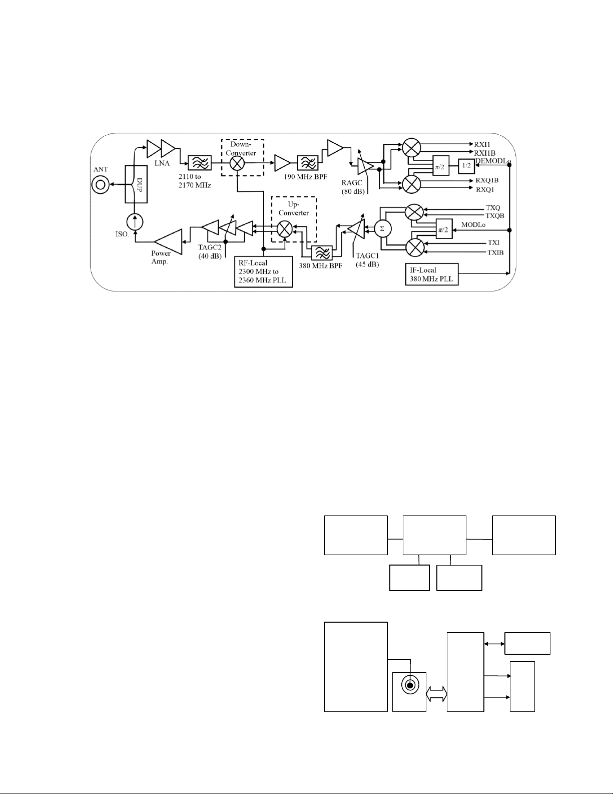
A block diagram of the transceiver using the
traffic demand is reaching over 200 megabytes per user, per
superheterodyne architecture is shown in Fig. 1. The system
month currently[2], and that one billion cellular subscribers
consists of up-link (transmitter) channel and down-link
will enjoy 3G services by 2010 [3].
(receiver) channel. The frequency range covered by the
The trend of future mobile communication applications transmitter is from 1920
will be a need for wideband mobile data networks with high
MHz to 1980 MHz. The RF input
frequency range of the receiver is from 2110
average throughputs and such networks can provide users MHz to 2170
MHz. A duplexer filter connects each channel to the antenna for
with wireless packet data access at peak rates up to from 384 full duplex operation.
kbps to 2 Mbps, even to 14.4 Mbps. In addition, these
applications need to be carried over efficient Internet protocol
2.1 Transmitter Channel
(IP) networks. As a result, all these requirements has been to
The transmitter is composed of intermediate frequency (IF)
provide the push to cellular operators to work efficiently on
local oscillator (LO), quadrature modulator, surface acoustic
migrating from current 2G/2.5G networks to the more
wave (SAW) bandpass (BP) filter, phase-locked RF LO, up-
efficient 3G networks and further to researchers to go beyond
converter, RF power amplifier, and two automatic gain control
original 3G technology targets [4].
(AGC) amplifiers before and after the up-converter,
As the need for low cost, low power consumption and high respectively.
performance user equipment is becoming important for
I/Q baseband signals are quadrature modulated with the
380 MHz signal of local oscillator. The modulated signal (380
Manuscript received March 5, 2007; revised May 20, 2007.
MHz) is adjusted in gain by TAGC1 and processed by SAW BP
KANG et al.: Preparation of Papers for Journal of Electronic Science and Techn ology of China (April 2004) 199 lOMoAR cPSD| 58977565
filter. The phase-locked LO up-converts the IF signal to the RF
2 stage RF low noise amplifiers (LNAs) providing total 30 dB
signal of 2300 MHz − 2360 MHz. In RF band, the signal is re-
of gain and filtered by the RF inter-stage filter at the LNA
amplified by TAGC2, RF driving circuit, and RF power
output. The IF SAW filter with low-pass impedance match is
amplifier and finally fed into antenna of the transmitter through
applied at the mixer output to suppress the LO fundamental. the duplexer.
Then the receiver path provides IF variable AGC amplifier and 2.2 Receiver Channel
quadrature demodulation functions to generate I and Q
Received signals from antenna are first amplified by the baseband outputs.
Fig. 1. The block diagram of the WCDMA transceiver. 3. Performance Test
The performance of the transceiver is measured on an
2.3 Design Considerations
evaluation board. The RF transmitting test system is shown in
For high performance purposes, the proposed transceiver
Fig. 2. Anritsu MG3861 generates a WCDMA signal fed into
is designed by a typical superheterodyne architecture. In such
RF subsystem. The Anritsu MS8609S is used to test the
a structure the input signal in each channel is mixed with a
transmitting power, error vector magnitude (EVM), adjacent
reference signal to produce a signal at desired frequency, which
channel power rejection ratio (ACPR), occupied bandwidth,
can then be filtered and processed. In more importance, the
and so on. The selection of RF channels and the setup of
superheterodyne structure provides good signal isolation to
transceiver enabling level are supplied by the controller.
both RF circuit and IF circuit, and provides the up-link and
The IF quadrature modulator gives 380MHz signal of −58
down-link high reliability of the RF front-end system.
dBm at 0.5 V or −13 dBm at 2.5 V to the TAGC1; the signal
The stability of signal leveling from AGC circuit is
level can be adjusted automatically in practical applications.
essential in high data rate designs, such as WCDMA system.
The two stages of AGCs (TAGC1 and TAGC2) supply the
Therefore, variable AGC amplifiers are used in up-link circuit
signal of total 85 dB gain. Table 1 summarizes the main
or down-link circuit to present required constant signal
measured performance of the transmitter channel.
amplitudes to their next stages. In transmitter channel, two
AGCs are used for large dynamic range of variable gain and MG3861 RF MS8609S
variable precision control, whereas in down-link design, the WCDMA subsystem transmitter test signal genertor
precise level from the RAGC allows full use of the input range of the baseband detection.
In addition, the SAW filters in the up-link and down-link DC Controller source
channels are utilized to improve signal quality and suppression
ability of the system. The common RF LO and IF LO are
Fig. 2. Test system for the RF transmitted output performance.
designed for the consideration of space saving and power
dissipation saving of the transceiver. Compared with zero-IF WCDMA f 2110
circuit scheme, which has DC-offset at the baseband output = MHz signal generator 2140MHz Controller
and therefore needs the cancellation of DC component, the 2170M Hz
designed structure gives an I/Q baseband output without any P-SCH= − 5 dB S-SCH= − d 5 B KIT DATA DC-offset. BOARD P-CCPCH= − 5dB P-CPICH= − 3dB BER CLK DPCH= − d 10 B RF-Board
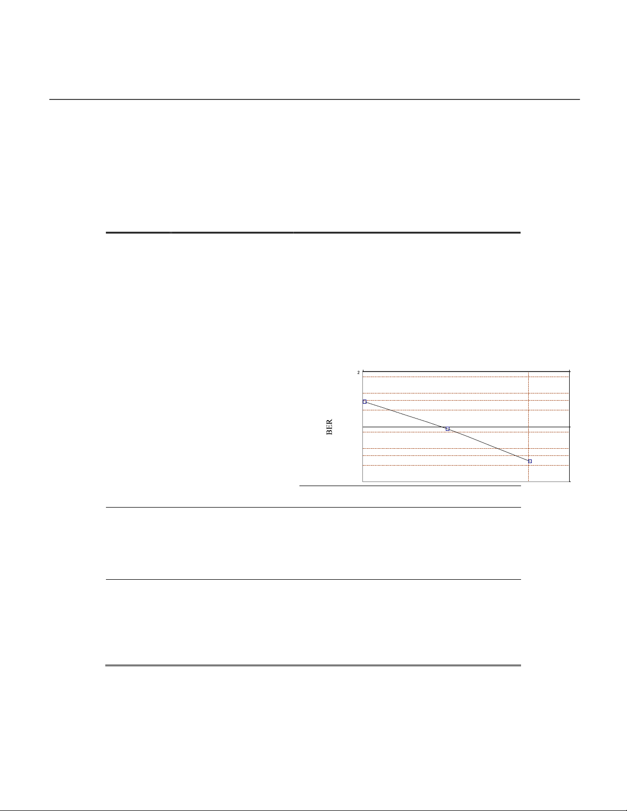
Fig.3. Test system for receiver performance. lOMoAR cPSD| 58977565
For receiver channel, the primary measurements are
2110 MHz − 2170 MHz. The tested result of our system in 2140
receiver sensitivity, adjacent channel selectivity (ACS),
MHz is −119.6 dBm/3.84 MHz (@BER=1×10⁻³), as 200
JOURNAL OF ELECTRONIC SCIENCE AND TECHNOLOGY OF CHINA, VOL. 5, NO. 3, SEPTEMBER 2007
intermodulation, blocking, and maximum receiver power
transmission, etc. Key features of the design include
level. Some of the test results of the receiver channel are given
superheterodyne architecture, AGCs design, and common
in Table 1. In our design, the main interest is in the receiver
local oscillators. The system has been implemented on an
sensitivity. According to the 3GPP specification [8], the
evaluation board. The performance test indicates that the
sensitivity at 1×10−3 bit error rate (BER) should be tested in
designed system is better compliant with WCDMA 3GPP standards. Table 1
Measured performance of the transceiver of Fig.1 shown in Fig. 4.
Compared with the required sensitivity of −117 dBm in
the 3GPP specification, the presented transceiver has a margin
about 3 dB and better than the result given in [6]-[7]. A proper
margin is valuable to cover the range of both basestations and
terminals, or to offer terminals longer standby-time in network. 4. Conclusion
A RF sub-system has been designed for third generation 22 1 × 10 −
WCDMA application. In a few years, such systems will
provide high-speed mobile access to Internet, video −20120dBm RF Input(dBm) −-119119d RF input (dBm) 1 × 10 33 −
Fig.4. The receiver sensitivity. System Specifications 1 × 10 44 − The proposed results The results of Ref. [6] Technology: Integrated Frequency range 1920 MHz−1980 MHz 1920 MHz−1980 MHz Circuits for Dynamic range 85 dB 50 dB Wideband Transmitter Maximum output power 22 dBm −41 6 dBm ACPR dB@5MHz 38 dB@1.92MHz EVM 6.7% ⎯ Frequency range 2110 MHz−2170 MHz 2110 MHz−2170 MHz Dynamic range 80 dB 80 dB Receiver sensitivity(@2140MHz) −119.6 dBm −115.4 dBm ACS(@2140MHz) -45.6 dBm ⎯ Overall NF 1.5 dB 4.0 dB I/Q gain mismatch ±0.5 dB 0.9 dB References
Communication and Wireless Sensor Networks, Singapore, 2005, pp: 21-25.
[1] T. Ojanperä, and R. Prasad, Wideband CDMA for Third
[3] D. L. Kaczman, M. Shah, N. Godambe, et al.; “A single-chip tri-
Generation Mobile Communications, Boston, London, Artech
band (2100, 1900, 850/800 MHz) WCDMA/HSDPA cellular House, 1999.
transceiver,” IEEE Journal of Solid-State Circuits, vol. 41, no. 5,
[2] W. Y. Ali-Ahmad; “Radio transceiver architectures and design pp. 1122-1132, May 2006.
issues for wideband cellular systems”, in Proceedings of IEEE
International Workshop on Radio-Frequency Integration lOMoAR cPSD| 58977565
[4] H. Honkasalo, K. Pehkonen, M. Niemi, and A. Leino; “WCDMA
and WLAN for 3G and beyond,” IEEE Wireless
Communications, pp. 14-18, Apr. 2002.
[5] S. K. Reynolds, B. A. Floyd, T. Beukema, et al., “A direct-
conversion receiver IC for WCDMA mobile systems”, IEEE
Journal of Solid-State Circuits,” vol. 38, no. 9, pp. 1555-1560, Sep. 2003.
[6] A. Pärssinen, J. Jussila, J. Ryynänen, et al., “A 2-GHz wide-band
direct conversion receiver for WCDMA applications,” IEEE
Journal of Solid-State Circuits, vol. 34, no. Measured data 12, pp. 1893-1903, Dec. 1999.
[7] K.-Y. Lee, S.-W. Lee, Y. Koo, et al., “Full-CMOS 2-GHz
WCDMA direct conversion transmitter and receiver,” IEEE
Journal of Solid-State Circuits, vol. 38, no. 1, pp. 43-54, Jan. 2003. [8] UE Radio Transmission and Reception (FDD),
Third-Generation Partnership, Project (3GPP), Tech. Spec. 25.101, v. 3.0.1, Apr. 2000.
Jing-Fu Bao was born in Zhejiang, China, in 1964. He received
the Ph.D. degree from University of Electronic Science and
Technology of China (UESTC) in 1996. From 1998 to 2004, he
worked with Sony, Japan as a senior engineer. Dr. Bao is a currently
professor with UESTC. His research interests include wireless
communication, signal analysis and processing, and IC designs.
Zhu-Sheng Kang was born in Jangsu, China, in 1957. He
received the Ph.D. degree from UESTC in 1988. From 1990 to 1992,
he was a research fellow with Birmingham University, U.K. and
Loughborough Technology University, U.K. From 1997 to 2003, he
worked with Infrared Engineering Co., U.K. and Sean-Tech Ltd. H.K.
as a senior engineer. He is a currently associate professor with UESTC.
His research interests include information processing, signal
processing, and techniques of high-speed digitalization.
Tài liệu liên quan:
-
Bài tập quy hoạch mạng hệ thống thu phát vô tuyến môn Thu phát vô tuyến | Học viện Công Nghệ Bưu Chính Viễn Thông
120 60 -
Tài liệu về RF transceiver architectures for W-CDMA systems like UMTS môn Thu phát vô tuyến | Học viện Công Nghệ Bưu Chính Viễn Thông
118 59 -
Tài liệu về Transmit diversity in 3G CDMA systems môn Thu phát vô tuyến | Học viện Công Nghệ Bưu Chính Viễn Thông
119 60 -
Chapter 6 WCDMA môn Thu phát vô tuyến | Học viện Công Nghệ Bưu Chính Viễn Thông
138 69 -
Tài liệu về Introduction to UMTS device testing môn Thu phát vô tuyến | Học viện Công Nghệ Bưu Chính Viễn Thông
119 60