Tài liệu về A Zero-IF 60 GHz 65 nm CMOS transceiver môn Thu phát vô tuyến | Học viện Công Nghệ Bưu Chính Viễn Thông
A Zero-IF 60 GHz 65 nm CMOS transceiver with direct BPSK modulation demonstrating up to 6 Gb/s data rates over a 2 m wireless link. Tài liệu được sưu tầm gồm 18 trang, giúp các bạn ôn luyện và phục vụ cho việc học tập, đạt kết quả tốt. Mời các bạn đón xem!
Môn: Thu phát vô tuyến (TEL1416) 10 tài liệu
Trường: Học viện Công Nghệ Bưu Chính Viễn Thông 1.8 K tài liệu
Tác giả:


Preview text:
lOMoAR cPSD| 58977565 2085
IEEE JOURNAL OF SOLID-STATE CIRCUITS, VOL. 44, NO. 8, AUGUST 2009
A Zero-IF 60 GHz 65 nm CMOS Transceiver With
Direct BPSK Modulation Demonstrating up to 6
Gb/s Data Rates Over a 2 m Wireless Link
Alexander Tomkins, Student Member, IEEE, Ricardo Andres Aroca, Takuji Yamamoto,
Sean T. Nicolson, Member, IEEE, Yoshiyasu Doi, and Sorin P. Voinigescu, Senior Member, IEEE
Abstract—This paper presents a directly modulated, 60 GHz
Digital Object Identifier 10.1109/JSSC.2009.2022918
zero-IF transceiver architecture suitable for single-carrier, low-
uncompressed high-definition video to the wireless replacement
power, multi-gigabit wireless links in nanoscale CMOS of next-generation wired interconnects, such as serial ATA and
technologies. This mm-wave front end architecture requires no USB 3.0. With such a wide-range of target markets, the
upconversion of the baseband signals in the transmitter and no
analog-to-digital conversion in the receiver, thus minimizing standards will have to be flexible enough to address the various,
system complexity and power consumption. All circuit blocks are and sometimes conflicting, performance specifications that
realized using sub-1.0 V topologies, that feature only a single high-
these applications will demand.
frequency transistor between the supply and ground, and which
It has become clear that one of the benefits that 60 GHz radio
are scalable to future 45 nm, 32 nm, and 22 nm CMOS nodes. The
transceiver is fabricated in a 65 nm CMOS process with a digital will present when compared to competing technologies, such as
back-end. It includes a receiver with 14.7 dB gain and 5.6 dB noise IEEE 802.11 and ultra wideband radios, is that the system-level
figure, a 60 GHz LO distribution tree, a 69 GHz static frequency complexity, and the amount of digital signal processing required
divider, and a direct BPSK modulator operating over the 55–65 to achieve equivalent data rates will be greatly reduced.
GHz band at data rates exceeding 6 Gb/s. With both the Singlecarrier systems with simple modulation schemes can be
transmitter and the receiver turned on, the chip consumes 374 mW
from 1.2 V which reduces to 232 mW for a 1.0 V supply. It occupies utilized and still achieve data rates in the multi-Gb/s range
1.28 0.81 mm . The transceiver and its building
blocks without the need for ADCs and DACs, all of which will
were characterized over temperature up to 85C and for power consume as much or higher power in a 60 GHz system than in
supplies down to 1 V. A manufacturability study of 60 GHz radio GHz-range radios. However, to take advantage of the potential
circuits is presented with measurements of transistors, the low-
complexity and power saving opportunities, appropriate
noise amplifier, and the receiver on slow, typical, and fast process
splits. The transceiver architecture and performance were transceiver architectures and circuit topologies must be
validated in a 1–6 Gb/s 2-meter wireless transmit-receive link over selected. the 55–64 GHz range.
This paper presents a system which has been tailored to
Index Terms—Millimeter-wave, nanoscale CMOS, 60 GHz, accommodate a simple modulation scheme that is appropriate
wireless transceiver, process variation.
for rapid file-transfer applications, thus simplifying its design
and allowing for a robust implementation, even in CMOS. This
architecture differs from other 60 GHz radio chip-sets reported I. INTRODUCTION
in SiGe BiCMOS [1] or CMOS [2]–[9], because it integrates a
fundamental frequency zero-IF transceiver, with a direct
HE mass market proliferation of mm-wave circuits is modulation transmitter. The system utilizes direct BPSK
Tr apidly approaching as multiple industry groups are now modulation at 60 GHz, precluding the need for a power
working to complete standards for the adoption of the 9 GHz of amplifier, a fundamental frequency static divider, and operates
bandwidth available worldwide between 57 GHz and 66 GHz. without requiring image rejection or ADCs in the receiver. The
The standards are devised to address numerous high-bandwidth transmitter input accepts baseband digital non-return-to-zero
applications, ranging from the streaming of
(NRZ) data at rates beyond 6 Gb/s, and the receiver outputs the
same digital data stream in NRZ format in a true, single chip
Manuscript received December 01, 2008; revised March 10, 2009. Current
bits-in/bits-out radio transceiver.
version published July 22, 2009. This work was supported by Fujitsu Limited.
Test equipment was provided under grants from CFI, OIT, and NSERC, and by
The paper is organized as follows. Section II presents the
the ECTI facility at the University of Toronto.
system design considerations and the transceiver architecture,
A. Tomkins, R. A. Aroca, and S. P. Voinigescu are with the Edward S. Rogers
and Section III describes the design of the various circuit
Sr. Department of Electrical and Computer Engineering, University of Toronto, Toronto, ON, M5S 3G4 Canada.
building blocks. The measured system characteristics are
T. Yamamoto and Y. Doi are with Fujitsu Laboratories Ltd., Nakahara-ku,
summarized in Section IV, and the results of a wireless link Kawasaki 211-8588, Japan.
demonstration are shown in Section V.
S. T. Nicolson was with the Department of Electrical and Computer
Engineering, University of Toronto, and is now with Mediatek, New York, NY 10007 USA.
II. TRANSCEIVER DESIGN CONSIDERATIONS
Color versions of one or more of the figures in this paper are available online
at http://ieeexplore.ieee.org.
Downloaded by Anh Tuyet (anhtuyet52@gmail.com)
swing constrained only by the reliability limit of the transistors. lOMoAR cPSD| 58977565
TOMKINS et al.: A ZERO-IF 60 GHz 65 nm CMOS TRANSCEIVER WITH DIRECT BPSK MODULATION 2086
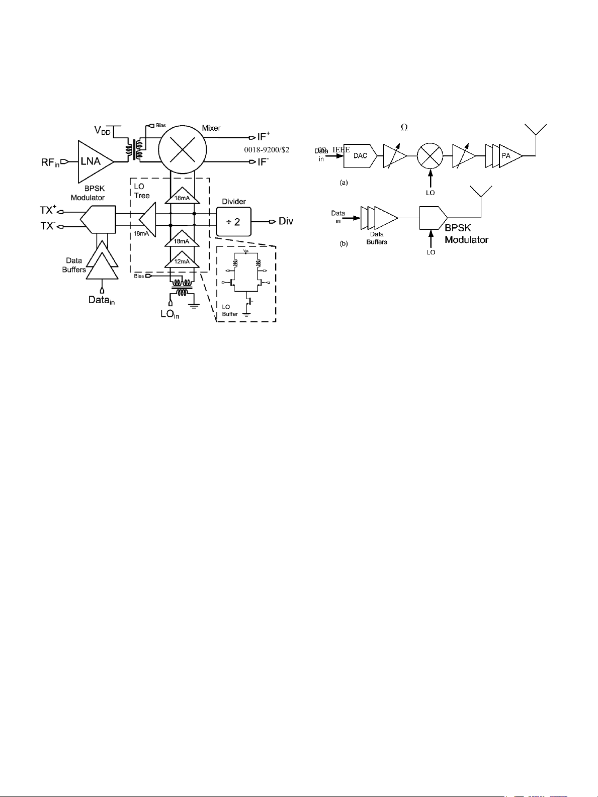
A block diagram of the proposed transceiver is presented in by operating the power amplifier backed-off several dB from
Fig. 1. NRZ data, produced off-chip, is applied to a largepower the saturated output power level and much below its peak 0018-9200/$26.00©2009 IEEE
Fig.2.(a)Conventionalup-conversiontransmitter.(b)Directdigitalmodula- tiontransmitter.
BPSK modulator which directly modulates the 60 GHz LO operating efficiency point. To achieve the required output power
signal and drives 50 loads differentially at the transmitter Fig. 1. levels with these restrictions in 90 nm CMOS, ever more
60 GHz direct modulation BPSK transceiver architecture.
complex designs have been considered, including distributed
power-combining with a 1.8 V supply [11] and beam forming
using as many as 36 individual transmitters on a single die [12].
output. The use of a single-phase modulation scheme in lieu of
A direct digital modulator/PA, Fig.2(b), addresses this
a multi-phase or quadrature technique reduces the system significant limitation by allowing the system to operate in
complexity and power-consumption required to distribute phase saturated mode, with maximum efficiency, and with the output
and amplitude matched quadrature signals throughout the chip. signal It also simplifies the baseband circuitry, which can be
To demonstrate the feasibility of integrating a fundamental implemented entirely digitally.
frequency PLL, the first stage of the pre-scaler, a novel
Unfortunately, this purely digital control also limits the type
quasistatic frequency divider, is integrated. The receiver of baseband pulse-shaping that can be performed to digital
consists of a high-gain, low-noise amplifier that drives a filtering [13] or delta-sigma oversampling [14] techniques, both
double-balanced Gilbert cell down-convert mixer. Because of which have been recently demonstrated in 2 GHz and 5 GHz quadrature
RF-DAC transmitters. Although this paper discusses direct
modulationwasnotemployedinthissystem,thereceivemixerissin
BPSK modulators only, ultimately any type of m-ary QAM, and
glephase. As well, the system transmitter generates a double even direct OFDM modulation, can be implemented using 2-6
sideband signal, negating any benefit of using an image reject binary-weighted unit cells, constructed from the BPSK
mixer. No IF amplifier was included, so it is important to note modulator presented here, connected in parallel, in a manner
that all the receive-path gain is at 60 GHz. The baseband NRZ similar to the digital-RF modulators in [13]–[15], with each
data is provided from off-chip to the transmitter and is BPSK modulator unit acting as a 1-bit 60 GHz DAC.
recovered at the IF output of the receiver, without any digital
In discussing potential modulation schemes, it is worth
signal processing or analog-to-digital conversion.
departingbrieflyfrom the coherentreceiverarchitectures,and
It is worthwhile to examine the benefits and disadvantages of consider that a low-power, low-cost option for the receiver is a
using a direct digital modulation architecture [10] as opposed to direct detection architecture (as in OOK systems [16] or remote
a more conventional direct-conversion transmitter consisting of sensing). However, if the same receiver sensitivity is to be
an up-converter followed by a power amplifier. The latter achieved, the RF filtering, and much higher gain and linearity
architecture, shown in Fig. 2(a), has numerous analog blocks, needed from the LNA to offset the high noise figure of the
each having to satisfy stringent linearity requirements. In detector, more than make up for the power savings obtained by
particular, the design of a 60 GHz power amplifier, which removing the down-convert mixer. Incidentally, a PLL is still
simultaneously delivers the high output power, high gain, and ultimately required in the transmitter.
high linearity that the various applications demand, represents
A link budget analysis for the short-range, file-transfer
one of the most serious challenges in mm-wave circuit design. application, employing a low-power transceiver with BPSK
The system-level linearity requirements are typically addressed lOMoAR cPSD| 58977565
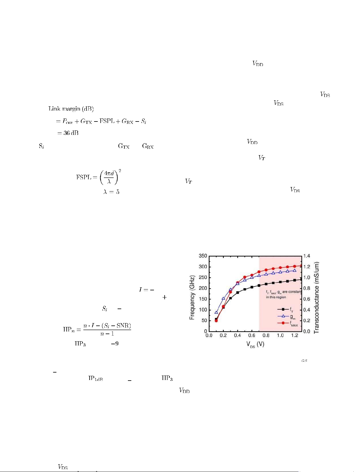
TOMKINS et al.: A ZERO-IF 60 GHz 65 nm CMOS TRANSCEIVER WITH DIRECT BPSK MODULATION 2087
modulation, provides guidance on the tradeoff between antenna variation. Stacked transistor topologies that place two or more
gain and the transmitter output power. Assuming a 2 m wireless highspeed transistors between and ground are particularly
link, 25 dBi transmit and receive horn antennas, 0 dBm susceptible to power-supply and process variation, and have
transmitter output power, 6 dB receiver noise figure and 4 GHz thus been avoided. As the measured characteristics in Fig. 3 bandwidth
illustrate, for large (0.8 V to 1.2 V), the performance of a
withanSNRof12dB,providesalinkmargin(withallthevalues
in transistor in terms of and , is relatively constant over dB or dBm):
variations. However, as the transistor drops to 0.5 V or
below, rapid performance degradation can be seen. Thus,
biasing transistors far from this sensitive area will ensure a more robust operation. (1)
Cascode topologies, which have at least two high-speed transistors stacked between and ground are vulnerable to
where is the receiver sensitivity and and are the gains of the power-supply and process variation due to the low of each
transmit and receive antennas. The free-space path loss (FSPL) transistor and the impact of the variation of the common-
is given by the classical formula:
gate MOSFET. Even when biased with the constant current
density biasing technique [17], which reduces circuit sensitivity
(2) to and bias current variations, threshold voltage variations in
which, for a 60 GHz signal with
mm, results in a path the common-gate transistor will still result in variation for loss of 74 dB over 2 m. the common-source MOSFET.
The relatively large 36 dB link margin can be used to increase
Looking beyond the immediate issue of susceptibility to
the link distance or can be consumed by the various setup losses power-supply and process variation, similar design
in an on-wafer wireless experiment, as in this paper. considerations will become more critical in future process
Alternatively,itcanbe tradedofffor lowcostand lowergain (10–
nodes. Scaled 32 nm and 22 nm nodes will require power
12 dB) PCB antennas, as demanded by a commercial, small supplies to be reduced from the levels in 65 nm CMOS, as
form factor 60 GHz radio. This analysis shows that the presence dictated by constant field scaling rules and device reliability
of the high directivity antennas relaxes the transceiver requirements. Using
specification sufficiently that only moderate transmit power and
good noise figure are necessary. Both requirements are easily
satisfied by 65 nm CMOS technology.
When the linearity of this transceiver was specified in March
2007, we considered the presence of an interferer 30 dBm
at the receiver input. This corresponds to a transmitter with 10
dBm output power located 10 cm away from the receiver.
Assuming a receiver sensitivity of 60 dBm, an SNR of 12 dB,
and using the well-known formula (3) becomes
the required receiver dBm. The current release of the
IEEE802.15.3c 60 GHz draft sets an even tougher specification
on receiver linearity by mandating operation at the nominal Fig. 3. Measured NFET transistor performance for constant V.
BER for a 10 dBm input signal. The latter pushes the minimum required receiver to at least 10 dBm and
topologies that place only one high-speed transistor between
to 0 dBm. These linearity figures are difficult to achieve without
consuming significant power in the LNA and in the receive
and ground is the only way to maximize the power gain as
mixer which drives 50 Ohm loads directly off chip.
well as minimize the noise figure of the transistor in future CMOS nodes. III. CIRCUIT BUILDING BLOCKS
All circuits employed in this system forego stacked transistor
topologies in favour of either transformer or capacitively
A principal design consideration for every block was to coupled cascode topologies that have no more than a single
ensure that they were robust to power-supply and process high-speed transistor stacked above a current source. These lOMoAR cPSD| 58977565
TOMKINS et al.: A ZERO-IF 60 GHz 65 nm CMOS TRANSCEIVER WITH DIRECT BPSK MODULATION 2088
topologies ensure operation from 1.2 or 1.0 V supplies, and desired operating frequency was used in anticipation of the
work equally well in LP, GP, or HP flavors of a 65 nm CMOS various layout parasitics that are not accounted for. The
process. LP, GP, and HP correspond to low-power, general-
calculated inductance is equally split into two parallel
purpose, and high-performance process variants of a CMOS inductances that are placed at the drain and source nodes
node, as described in [18]. These options are typically respectively. For example, the drain inductance of the first
distinguished from each other based on the effective gate length stage, and the source inductance of the second stage are
and oxide thickness, with HP having the thinnest oxide, and the calculated to resonate with the parasitic capacitance of shortest gate length. transistors M1 and M2, given
The penalty for using AC-coupled cascodes is a doubling of
current consumption compared to the traditional telescopic
cascode [19], which is only partially compensated by the
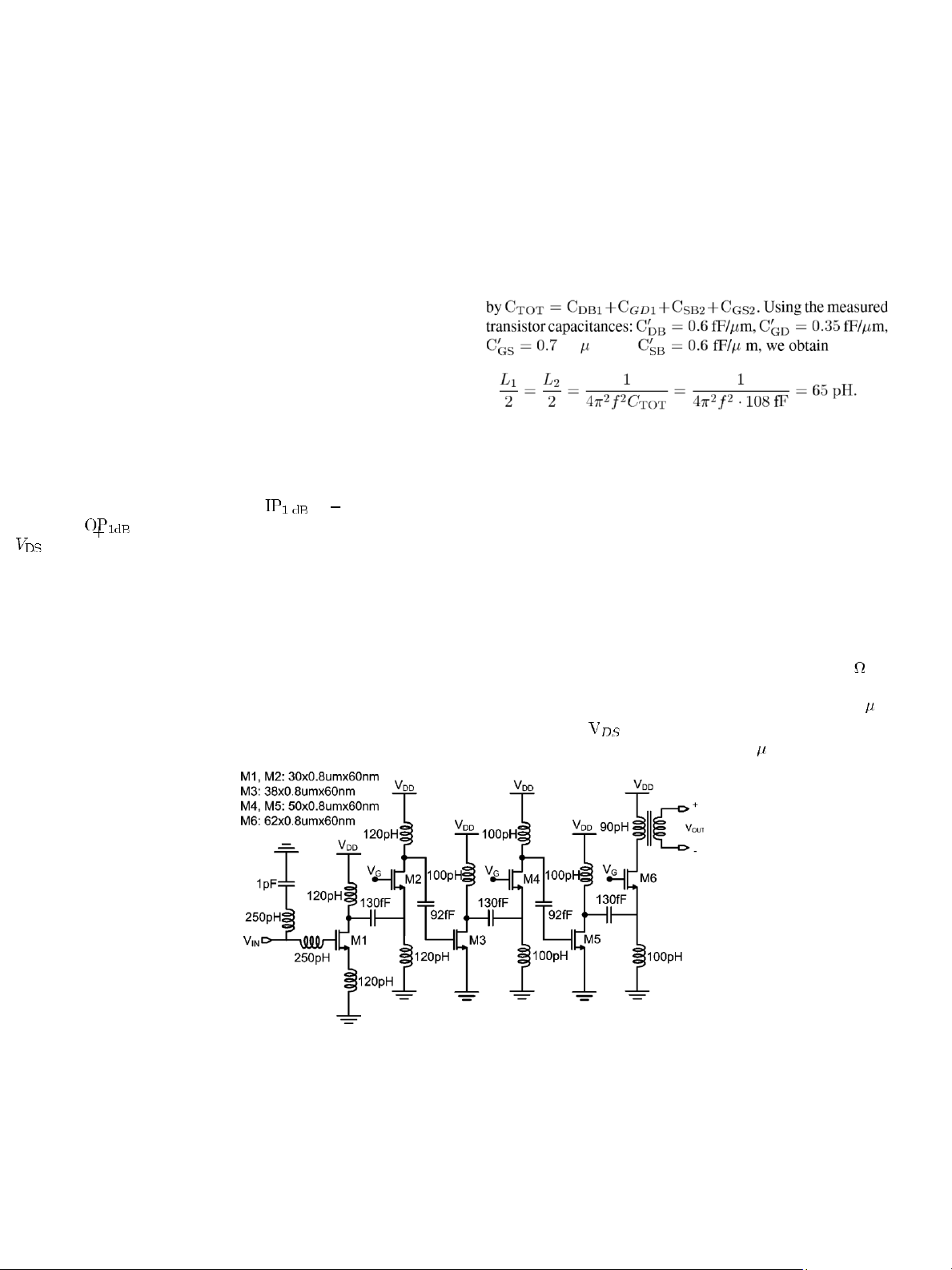
potential reduction in power supply voltage. A. Low-Noise Amplifier fF/ m, and
TheLNAschematicisshowninFig.4.Itconsistsofthreecascaded
CS-CG stages, with the minimum gate length transistors and (4)
with increasing gate width from stage to stage. The most
important design goals were a power gain of at least 20 dB, a
noise figure below 6 dB, and an of 15 dBm which sets the to at This corresponds to an effective inductor value of 130 pH, and
least 4 dBm. The gate width and bias current of the MOSFET allowing for an approximate 10% shift in center frequency due
in the last stage is determined by the output compression point, to un-modeled parasitic capacitances, 120 pH inductors were
while the gate width and bias current of the first stage MOSFET implemented.Forlaterstages,inwhichthe MOSFETgatewidth is
is calculated to minimize noise figure and to satisfy the larger, the inductor sizing was not scaled down at an equal rate,
simultaneous noise and input impedance match condition [19]. creating a slight staggering in the center frequency of each stage
The design of the LNA proceeds according to the and thus broadening the frequency response of the entire
methodology described in [19] for telescopic cascodes, with amplifier.
modifications to accommodate the AC-coupled cascode
The input stage is noise and impedance matched to 50 , as
topology. The load inductance of the CS stage and the source in a telescopic cascode stage [19], and is biased at the minimum
inductance of the CG stage are determined from the condition noise figure current density, which corresponds to 0.3 mA/ m
that, in parallel, they resonate with the total capacitance at the for a transistor
of 1.2 V. All transistor layouts feature
common node of this cascode at the center frequency of the minimum gate length nMOSFETs with 0.8 m finger width and
Fig. 4. 1.2 V, three-stage cascaded CS-CG, 60 GHz low-noise amplifier schematic.
amplifier. Device capacitancesat the drainnode ofthe double-sided gate contacts. The last stage of the LNA is loaded
CStransistorand at the source of the CG transistor, the parasitic with a transformer which acts as single-ended to differential
capacitance of the inductor, as well as the bottom-plate converter between the LNA and the double-balanced mixer. The
capacitance of the AC-coupling MiM capacitor, all contribute LNA, which can also be operated as a low-noise, moderate
to the total node capacitance. For initial hand-derived power amplifier, consumes 80 mA (60 mA) from a 1.2 V (1.0
parameters, a center frequency of 66 GHz, 10% above the V) power supply. It should be noted that the power consumption lOMoAR cPSD| 58977565
TOMKINS et al.: A ZERO-IF 60 GHz 65 nm CMOS TRANSCEIVER WITH DIRECT BPSK MODULATION 2089
of the LNA could be reduced by scaling down the size and bias telescopic cascode) while operating, like the CS stage, with a
currents in the last four stages without affecting the overall low-voltage supply.
noise figure and gain. However, as discussed in Section II, the
input compression point would be negatively affected. B. BPSK Modulator
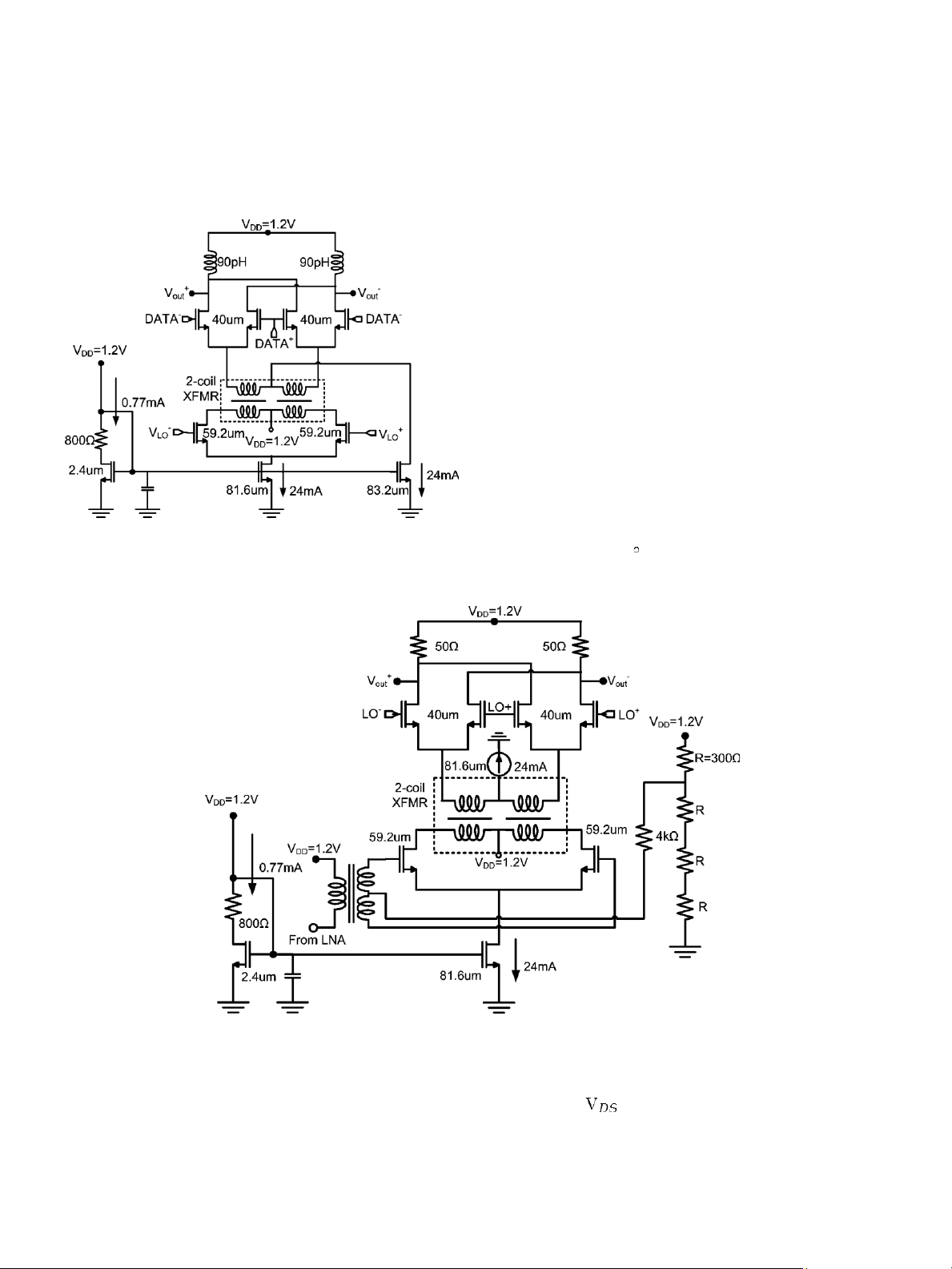
Fig. 5 illustrates the schematic of the BPSK modulator. All
transistors have minimum gate length. This topology allows for
the direct modulation of the 60 GHz carrier by a large-swing
data signal with no concern for signal linearity at the LO port.
Historically, the first direct BPSK modulators featured balanced
switches realized with PIN or Schottky diodes and diode
bridges, but implementations in GaAs MESFET [20], CMOS or
SiGe BiCMOS technologies permit the use of the active Gilbert
cell. The data signal is applied to the gate of the mixing quad
transistors, while the carrier (LO) signal is injected as Fig. 6. Mixer schematic.
current, differentially, to the sources of the Gilbert-cell quad.
The mixing-quad transistors act like switches, directing the LO
current either to the positive or to the negative output node thus
Fig. 5. BPSK modulator schematic.
introducing the 0–180 phase modulation. Direct mm-wave
BPSK modulators based on this topology have been reported at
Finally, it is worth noting the reasons for implementing an 65 GHz [21] and 77 GHz [22] in SiGe HBT technology, aand
AC-coupled cascode topology rather than a simple cascade of similar topologies have been applied recently in direct-digital
common-source (CS) stages. The CS topology with inductive RF modulators in the 1–5 GHz range [13], [14].
load is known for its potential instability and propensity to
Transformer coupling has been employed to AC-couple the
oscillate. Furthermore, its poor isolation at mm-waves makes it LO signal from the transconductor pair into the Gilbert cell, thus
difficult to design a multistage amplifier, or an entire receiver, maximizing the
(approximately 0.9 V) of the mixing quad
when models are inaccurate or process variation is a concern, as transistors and the output power. Since the output transistors act
in this case. The AC-coupled cascode avoids all of these as large power switches, the modulator can be viewed as a
problems due to its excellent isolation (similar to that of a switching PA. As long as the LO signal applied to the modulator lOMoAR cPSD| 58977565
TOMKINS et al.: A ZERO-IF 60 GHz 65 nm CMOS TRANSCEIVER WITH DIRECT BPSK MODULATION 2090
maintains 50% duty cycle and does not exceed the input
compression point of the switch, the EVM of the output
spectrum is insensitive to the LO amplitude, temperature, and LO frequency.
The differential modulator output features 90 pH inductors
which tune out the transistor and output pad capacitance. The
gate width of the MOSFETs in the BPSK modulator is chosen
such that the real part of the output impedance at resonance is
approximately 60 while is 75 . This simple, relatively wideband,
matching is provided by the DC output resistance of the MOSFETs [19].
As in CML gates, the current density through the modulating
switches changes from 0 to 0.3 mA/ m [17]. If we consider that
all transistors are biased at 6 mA each, or 0.15 mA/ m, we can
estimate the output power of this modulator. Assuming a 0.3 V
drop across the tail current source, and a minimum of 0.15 V
across a fully on transistor, we can expect a maximum
theoretical amplitude swing of 0.75 V, or 1.5 . This
corresponds to a maximum differential output power of (5)
If we account for a 2 dB loss due to the output matching
network, we arrive at a figure of 4.5 dBm. The latter is
confirmed by simulations after layout parasitics extraction
which show a voltage swing of 0.9 per side corresponding to a
differential output power of 2.7 mW or 4.3 dBm. C. Mixer
The mixer schematic, shown in Fig. 6, is essentially identical
to that of the BPSK modulator. Due to lack of time at the design
phase, and because it has to drive 50 loads off chip with a large swing of 0.6
per side, the mixer was simply a copy of
the BPSK modulator. All components, sizes, and bias currents
are identical. The transistors in the mixing quad are biased at
0.15 mA/ m for maximum switching speed while those in the
differentialtransconductor are biasedat 0.2mA/ m.
Thesingleended signal from the LNA is converted to differential
mode by the load transformer in the output stage of the LNA
(shown in this figure), and drives the transconductance pair of
the mixer. Transformer coupling is again used to convert the RF
signal into an AC current that is injected into the sources of the
mixingquad using a 28 m, two-coil, vertically-stacked
transformer. The mixing-quad transistors are driven directly by
an 18 mA LO-tree buffer. This topology has been shown to be
scalable up to at least 140 GHz in CMOS [23].
No IF amplifiers were implemented in this system. lOMoAR cPSD| 58977565
TOMKINS et al.: A ZERO-IF 60 GHz 65 nm CMOS TRANSCEIVER WITH DIRECT BPSK MODULATION 2091
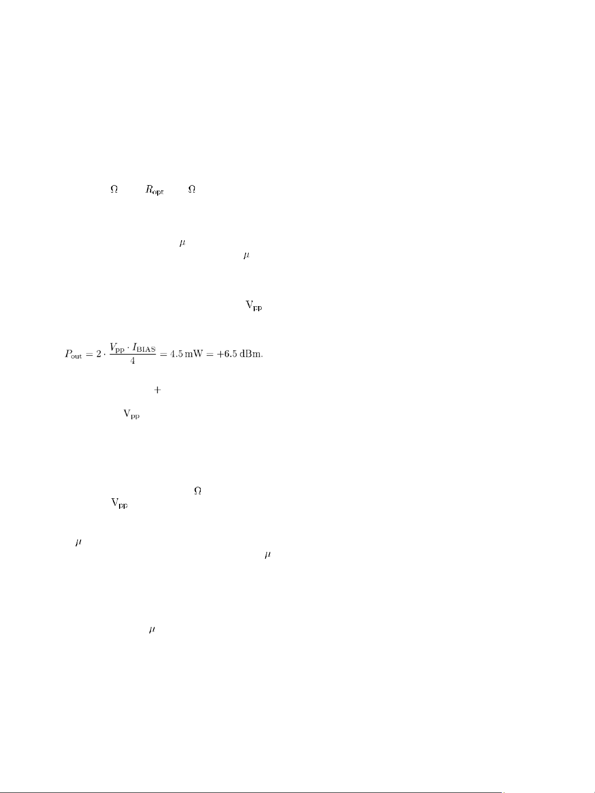
Fig. 7. Static frequency divider schematic (top), and layout details of the divider core (bottom).
D. Quasi-Static Frequency Divider
Static frequencydividersbasedona CML latch topologywith stacked high- and low- MOSFETs have been
The fundamental frequency divider represents one of the key demonstrated at frequencies exceeding 90 GHz [27], [28].
blocks required for the successful integration of a fundamental However, their operation range is greatly diminished at 100 C
frequency synthesizer. CMOS mm-wave VCOs in the V- and [25] and vanishes at 1.0 V supply. In this paper we propose an
W-band, simultaneously generating 0 dBm output power and alternate static-divider topology that is more suitable for low
exhibiting phase noise values lower than 90 dBc/Hz at 1 MHz voltage operation. Its schematic is shown in Fig. 7 (top). It
offset, have already been demonstrated [24], [25]. While their features a single differential pair at the clock input which drives
tuning range is lower than 10%, coverage of the entire 57–66 the two latches through two 28 m 28 m transformers. This
GHz band can be provided by a bank of frequency-spaced effectively eliminates one of the two clock differential pairs
VCOs [26]. A static-like frequency divider guarantees a wide resulting in a reduced area and power consumption, while also
operating frequency range, which is essential in a 60 GHz PLL. permitting operation without multiple transistors and s
A narrowband injection-locked divider, for example,
significantly complicates the PLL design where tracking of the between
and ground. The size and bias current of the eight
VCO and divider over the full frequency band must be ensured transistors in the latches, the load resistors, and the load inductor
over temperature and process variation [26].
values are identical to those of the 90 GHz CML divider in [27].
The transformers were realized with two vertically stacked coils lOMoAR cPSD| 58977565
TOMKINS et al.: A ZERO-IF 60 GHz 65 nm CMOS TRANSCEIVER WITH DIRECT BPSK MODULATION 2092
with inputs and outputs aligned along a diagonal line of of fingers in half while maintaining the same total gate width. symmetry.
This has the net result of further reducing the parasitic
Fig. 7 (bottom) illustrates the layout detail including the first capacitances of the device and thus increasing .
of three CML buffers at the divider output.
In order to minimize the layout parasitic capacitances of the E. Tuned Clock Tree
latch, which are known to be an important factor in determining
the self-oscillation frequency of mm-wave dividers, [27], an
The design of the LO tree represents one of the main
challenges in achieving large-scale system integration at 60
GHz. While this transceiveris intended tooperate witha
fundamentalfrequency PLL synthesizer, we note that a 60 GHz
LO distribution network is needed even if the VCO signal is
provided by a multiplier chain or by a second harmonic VCO
[29]. In this transceiver, a tuned LO distribution tree with 25%
bandwidth was designed. It consists of a cascade of differential
buffers with inductive loads and a fanout of two or three, as
shown in the inset of Fig. 1. Since the maximum available
power gain of a 60 nm nMOSFET is 10–11 dB at 60 GHz, and
since the LO buffers are meant to operate with large input and
output voltage swings, the voltage gain is about 1 while the
current gain cannot exceed 3. Hence, the maximum fanout in
the LO tree is limited to 3. Both 12 mA and 18 mA buffers are
employed. These relatively large currents are needed to drive
the 24 mA BPSK modulator in the transmitter, the 24 mA
receiver mixing quad, and the 18 mA divider stage. The
MOSFETs in the buffer are biased at 0.3 mA/ m for maximum
linearity [19]. An on-chip transformer balun is employed to
convert the single-ended external LO signal to differential mode
at the input to the first buffer.
A VCO or PLL was not implemented in this transceiver.
However, whether the choice is made to design a larger, high-
power fundamental frequency VCO [25], a multiplier chain
which is able to generate much of the required LO power [1], or
a small, low-power oscillator/multiplier that requires significant
signal gain in the LO tree in order to provide sufficient power
to the critical blocks, the power-consumption burden will still
exist, and has simply been shifted between different blocks.
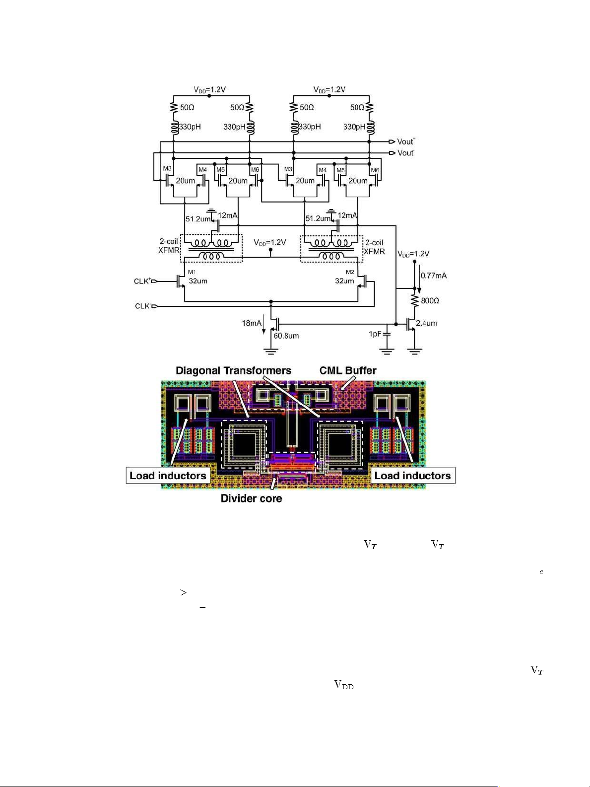
Fig. 8. Illustration of the unit-cell layout of the latch in the divider. Each
connection of the latch unit-cell is identified, and the merged, inter-digitated
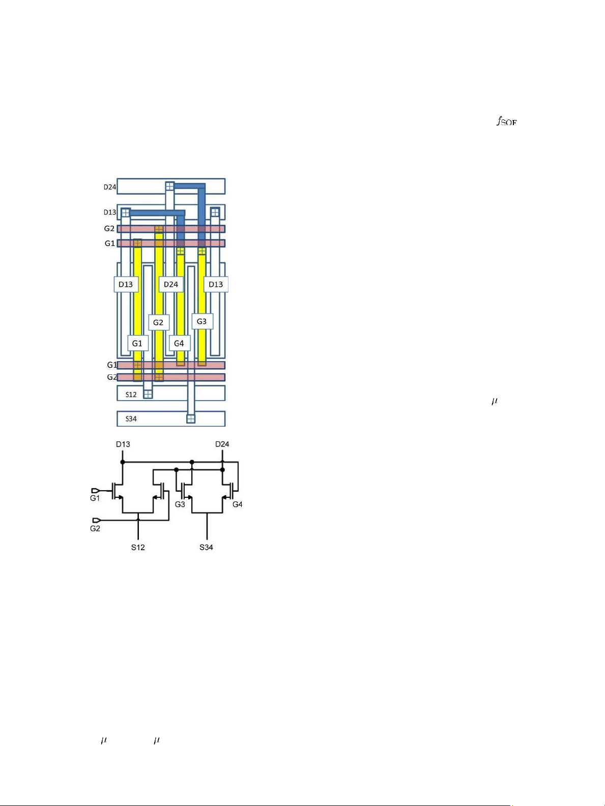
F. Tuned mm-Wave Switch arrangement can be seen.
While not included in the transceiver, a stand-alone 50–70
innovative and compact latch layout was utilized here. Fig. 8 GHz series-shunt switch, shown in Fig. 9(a), was designed and
shows a diagram of the layout for the unit-cell that is used to manufactured on the same dies and characterized separately.
build the entire latch. Each of the unit-cells contains one finger Passive switches exhibit excellent linearity without consuming
for each of the latch transistors, and all of the required power [30]. They can provide important functions such as on-
connections. A cascade of these unit-cells is employed to build chip calibration [31] and transmit/receive antenna sharing [32],
the entire divider latch. By merging the 4 MOSFETs together both critical features facilitating the successful
and inter-digitating the fingers, the loop-delay time due to long commercialization of mm-wave systems, permitting low-cost
inter-connect, as well as the output differential-mode at-speed testing and reducing the number of expensive off-chip
capacitance are reduced and the maximum frequency of 60 GHz components.
operation is increased. Similarly, by increasing the unit finger
For a series-shunt switch topology, the trade-offs between the
width up to 1.6 m from 0.8 m, it is possible to cut the number achievable insertion loss and isolation are well known [33], and lOMoAR cPSD| 58977565
TOMKINS et al.: A ZERO-IF 60 GHz 65 nm CMOS TRANSCEIVER WITH DIRECT BPSK MODULATION 2093
come as a result of the presence of the various parasitic
capacitances, as illustrated in Fig. 9(b). Wider series MOSFETs
exhibit smaller ON-resistance and will initially reduce the
insertion loss, but the parasitic capacitances will eventually
begin to increase the insertion loss while also degrading the
isolation. Similarly, the shunt MOSFET ON-resistance
increases the effective isolation, but the associated shunt
parasitic capacitance will degrade the insertion loss. To
minimize the ON-resistance (about 370 m in 65 nm CMOS
[30]) both transistors have minimum gate length. A technique
used to mitigate the performance degradation caused by (7)
parasitic capacitances, is to use inductors to resonate with the
parasitics [34]. Placing a series inductor, , across the series MOSFET, and a shunt inductor, fF/ m, and
, acrossthe shunt MOSFET, willreduce the insertionloss,
and increase the isolation respectively.
These structures can be modeled using the ON and OFF state
. By independently sweeping the
models shown in Fig. 9(b). The measured MOSFET device widths of the shunt and series transistors, the trade-off
capacitances at V are employed to determine and
between insertion loss and isolation can be simulated, and
device sizing can be selected.
This design aimed for the largest possible isolation while still maintaining less mand than 3 dB insertion fF, loss. This lead to m, which correspond to
fF. After layout parasitic extraction and
inductor modeling, additional adjustment of the inductors was
required to arrive at the final values of pH, and
pH, as illustrated in Fig. 9(a).
The switch is controlled by complimentary signals that bias
the gates through large resistors that prevent oxide breakdown
and ensure that the gate acts as an AC-floating node, thus
minimizing signal loss through parasitic gate coupling.
Fig. 9. Schematic of the 60 GHz tuned series-shunt SPST switch (top) and the
transistor equivalent models used for hand-design and simulation (bottom).
. From the schematic, the parasitic capacitances are given by
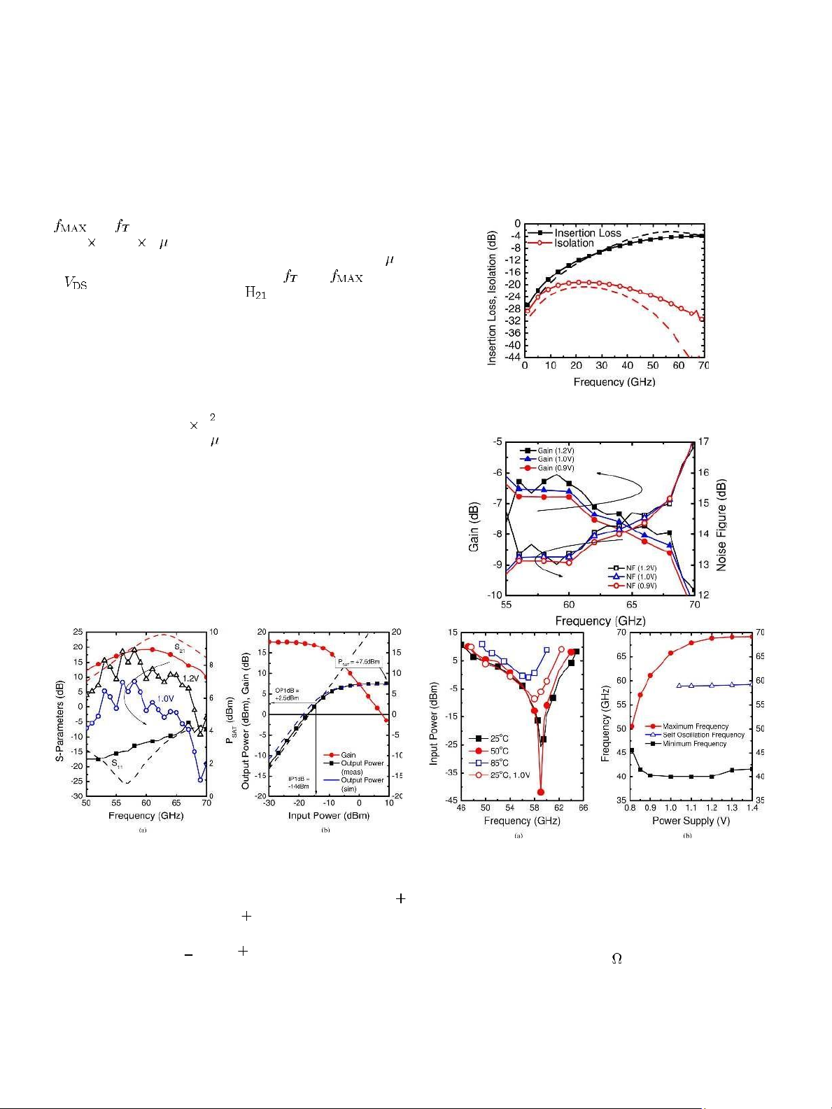
Fig. 10. Die photograph of the transceiver. Total die area is 1.28 0.81 mm. lOMoAR cPSD| 58977565
TOMKINS et al.: A ZERO-IF 60 GHz 65 nm CMOS TRANSCEIVER WITH DIRECT BPSK MODULATION 2094 IV. EXPERIMENTAL
insertion loss of 3.9 dB and an isolation of 28 dB at 60 GHz.
The simulated characteristics follow measurements quite well,
A. Chip Implementation and Layout
Fig. 11. Measured results of the LNA breakout. (a) S-parameter measurements
(with simulated results in dashed lines) and saturated output power results over
The transceiver was fabricated in a 65 nm CMOS process frequency (b) LNA linearity at 59 GHz with the simulated output power shown as a dashed line.
with a 7-metal digital back-end and MIM capacitors. Peak and
values of 300 GHz and 220 GHz were measured on 80 60 nm 1
m nMOSFETs with double-sided gate contacts, at current
densities of approximately 0.3 and 0.4 mA/ m respectively with a
of 1.0 V. The and values were extracted from the
measured and the unilateral power gain in the 1 GHz to 67 GHz
range using an Agilent 67 GHz PNA. The S-parameters and
maximum available gain were also measured in the 55–95 GHz
range with a Wiltron 360 B VNA. The input and output
parasitics (pad and interconnect) were de-embedded using the
T-line procedure described in [35]. A microphotograph of
the transceiver is shown in Fig. Fig. 12. Measured insertion loss and isolation of the 60 GHz series-shunt SPST 10. It occupies 1.28
0.81 mm . The LO and RF switch with simulation results shown as dashed lines.
signals are distributed along -strip lines formed in metal 7 over
a shunted metal 1 and metal 2 slotted ground plane. A grounded
side-wall consisting of p-substrate taps and all metals shunted
together forms a Faraday cage-like structure around each
transmission line [36] and between circuit blocks, improving isolation.
B. Test Structure and Transceiver Measurements
S-parameter measurements of the LNA breakout, shown in
Fig. 11(a) along with simulated results as dashed lines, display
a peak gain of 19.2 dB at 60 GHz and a 3 dB bandwidth Fig. 13. Measured gain and noise figure of the stand-alone 60 GHz mixer for
extending from 54 GHz to 66 GHz. The return loss is better than 1.2, 1.0, and 0.9 V power supplies.
10 dB up to 66 GHz. The saturated output power of the LNA,
measured in a large-signal measurement setup, is greater than
with the largest error observed for isolation. The latter could be
7.5 dBm with a 1.2 V supply and 5 dBm with a 1.0 V supply. due to an optimistic Q value for the modeled inductors.
Fig. 11(b) shows the measured input- and output-referred 1 dB
A breakout of the mixer was tested using an Agilent Noise
compression points of 14 and 2.5 dBm, respectively. The Figure Analyzer. The gain and 50 noise figure measurements
simulations and measurements of the linearity agree within the are compiled in Fig. 13. It should be noted that the mixer
measurement uncertainty of 1 dB.
employs a double balanced topology, requiring differential LO
The measured S-parameters of the stand-alone mm-wave and RF signals. These differential signals were produced on-
switch are presented in Fig. 12. The switch achieves a nominal chip using integrated transformers whose losses degrade both lOMoAR cPSD| 58977565
TOMKINS et al.: A ZERO-IF 60 GHz 65 nm CMOS TRANSCEIVER WITH DIRECT BPSK MODULATION 2095
the noise figure and the down-conversion gain. These losses
were not de-embedded from the reported measurements.
The static frequency divider sensitivity was measured in the
transceiver and includes the effect of the LO distribution net-
Fig. 14. Measured (a) divider and LO-tree sensitivity, and (b) divider (breakout)
frequency range over power supply.
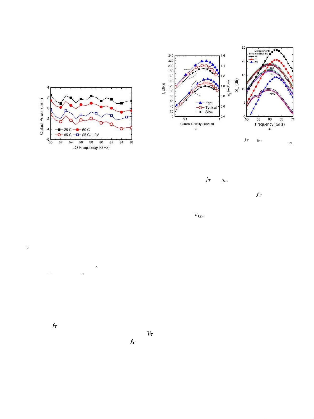
Fig. 16. Measured (a) NFET 80 1 m 60nm and , and (b)LNA
over fast, typical, and slow process corners. Measured LNA results are shown
as lines, with simulated results for the same corners, shown as lines with
Fig. 15. Measured transmitter output power as a function of LO frequency and symbols. over temperature.
observed from the fast to typical process lots can be seen to
work. The self-oscillation frequency is 59.2 GHz at room-
track the variation in and , cumulated over 6 gain stages.
temperature with a 1.2 V supply. As illustrated in Fig. 14(a), the However, the drop in the slow corner (9–10 dB) exceeds the
divider operates over a frequency range of 46–65 GHz at 1.2 V, equivalent decrease observed in the transistor measurement.
and 47–62 GHz at 1.0 V. To remove the impact of the LO tree This increased degradation can be attributed to an error in the
on the measured performance of the divider, the latter was tested biasing of the common-gate transistors in the LNA, which were
on a breakout version of the divider. Fig. 14(b) shows the biased at a fixed
, rather than at constant current-density. As
maximum, minimum, and self-oscillation frequency of the the transistor parameters vary over the process corners, the
divider breakout measured as a function of the power supply threshold voltage is seen to increase in the slower corners. This
voltage. When the power supply is reduced to 0.9 V, the divider ultimately results in a severe under-biasing of the common-gate
operates from 40 GHz to 61 GHz. Under nominal conditions transistor in the slow process corner, leading to the observed
(25 C, 1.2 V) the divider operates from 40 GHz to 69 GHz. performance degradation. Themeasuredtotal integratedpowerat the outputofthe
FromtheLNAgainmeasurements,weobservethatthereisno
transmitter is plotted in Fig. 15 versus frequency. Measurements impact of process variation on the center frequency of the LNA.
are shown over temperature up to 85 C, with a maximum output Thelatterisdeterminedbytheextrinsicdeviceparasitics(metalizati
power above 2.4 dBm at 25 C and 58 GHz.
on capacitance, resistance and inductance) and the discrete C. Process Variation
tuning elements (inductors, capacitors, etc) which do not vary
in these corners lots. This explains why the hand design
The manufacturability of the 60 GHz transceiver was studied equations, along with well modeled inductors, are almost as
by measuring transistors, the low-noise amplifier, and the accurate as the transistor models (within 5% of the measured
standalone receiver on 16 dies that were deliberately fabricated center frequency). The conclusion is that the main impact of the
on wafer splits representative of the slow, typical, and fast process variation in these tuned circuits is in the peak
process corners. Results in Fig. 16(a) indicate a 10% drop in transconductance value, and hence in the power gain. Although
transistor peak from the fast to typical corner splits.
the simulated LNA gain tracks the measurements across process
It should be noted that, although there is significant
corners, it is optimistic and shifted to higher frequencies by 5–
variation between corners, the measured peak
current 6%. The frequency shift is consistentwith the expectationsmade
density remains essentially constant. The measured LNA gain during the initial design phase.A5–
is plotted in Fig. 16(b) over process corners, along with the 10%errorinthevalueofthepassivecomponentscan account for the
simulated performance over the same corners. The LNA gain observed shift. In fact, the main culprit for the reduced gain degradation
observed in measurements can only be explained by series
resistive and inductive parasitics at the top level layout or by
underestimated parasitic capacitance in the extractor or in the
inductor models. The latter two are very difficult to measure at lOMoAR cPSD| 58977565
TOMKINS et al.: A ZERO-IF 60 GHz 65 nm CMOS TRANSCEIVER WITH DIRECT BPSK MODULATION 2096
60 GHz. We note that simulation after top level dummy fill and due to transistor and degradation. As in the LNA, the peak gain
resistive parasitics extraction was not performed due to the large frequency of the receiver and the minimum noise figure
number of circuit elements. A 0.5–0.8 dB gain reduction per frequency are not affected by process variation.
LNA stage due to top level layout parasitics is sufficient to
Finally, it should be noted that, despite the significant drop in
account for the discrepancy between the measured and the LNA performance from the fast to the slow process corner (9–
simulated peak gain of the LNA.
10 dB), the receiver noise figure increases by less than 2 dB
It should be noted that, compared to the standalone receiver (from 5.6 to 7.1 dB). This is a direct consequence of the
breakout measurements, the receiver gain measured in the trans- nominally large gain of the LNA. Although additional power
consumption was required in order to design an LNA with high
nominal gain, it appears to be the only feasible approach to
address the large expected process variation of nanoscale mm- wave CMOS circuits.
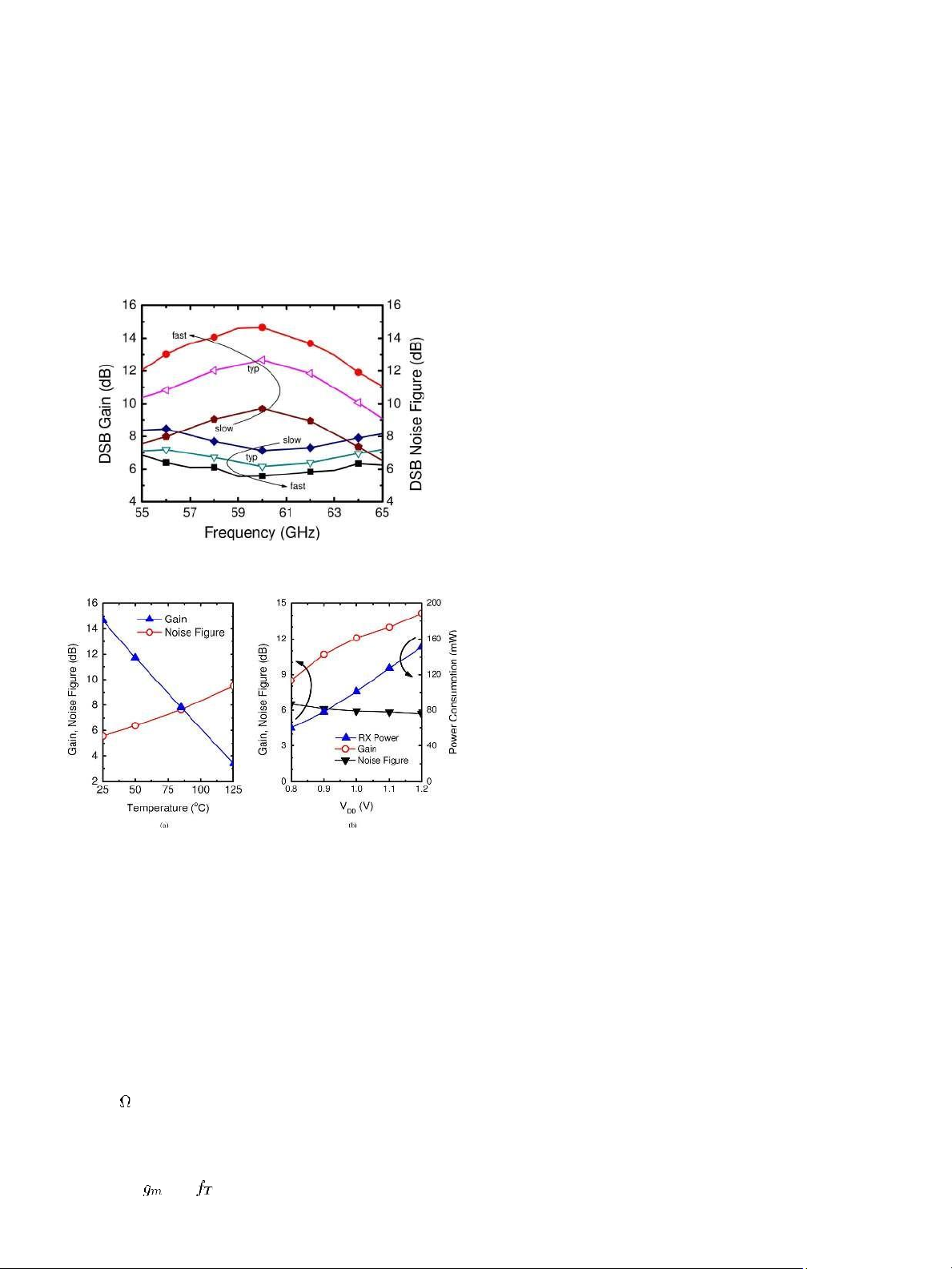
Fig. 17. Measured receiver (breakout) gain and noise figure over fast, typical, and slow process corners.
Fig. 18. Measured receiver gain and noise figure over (a) operating temperature, and (b) power supply.
ceiver was degraded by 3 dB because of insufficient LO power
at the mixer LO port. The LO-tree fanout in the transceiver is 3,
whereas it is only 1 in the receiver breakout. Performance
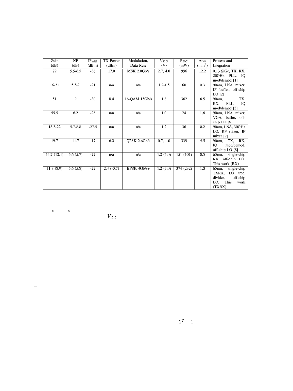
results for both versions are summarized in Table I at the end of
this paper, but the following results are for the receiver only.
The receiver gain and noise figure are plotted in Fig. 17 for the
fast, typical and slow corners. Measurements were carried out
using an Agilent Noise Figure Analyzer with a Noisecom V-
Band noise source. A peak receiver conversion gain of 14.7 dB
and a 50 noise figure of 5.6 dB are noted, both occurring at
60 GHz. The DSB noise figure remains below 6 dB over an RF
bandwidth of 58 to 63 GHz. The receiver measurements
indicate that the impact of process variation on the receiver can
be, for the majority, attributed to LNA performance decrease lOMoAR cPSD| 58977565
TOMKINS et al.: A ZERO-IF 60 GHz 65 nm CMOS TRANSCEIVER WITH DIRECT BPSK MODULATION 2097 TABLE I
PERFORMANCE COMPARISON FOR 60 GHZ TRANSCEIVER/RECEIVER CHIP-SETS.
BRACKETS SHOW MEASURED RESULTS FROM 1.0 V
Measurements of the receiver over temperature in Fig. 18(a) receive link was demonstrated in the 55–64 GHz range by
showapproximately7dBgaindegradationand2dBnoisefigure
employing one transceiver chip in transmit-mode mounted on a
increase from 25 C to 85 C. Fig. 18(b) illustrates that the gain probe station, and another transceiver chip in receive-mode
and noise figure do not seriously degrade as
is reduced to placed on a second probe station, approximately 2 meters away.
1.0 V, with a gain drop of 2.5 dB, and a noise figure increase of A schematic of the experimental setup is shown in Fig. 19. The
only 0.3 dB. When operated from 0.8 V supply, the receiver still circuits were contacted using 67 GHz signal probes and 67 GHz
has 9.8 dB of conversion gain, and a 6.5 dB noise figure, cables connecting to horn antennas with 25 dBi gain. An
illustrating the relative immunity of this design to power supply external amplifier with 30 dB gain and 4 GHz bandwidth was
variation. While the gain degradation over temperature and connected between the IF output of the receiver and a sampling
supply can beeasily compensatedfor at IFwitha VGA,thenoise-
oscilloscope (Agilent 86100C-DCA). The phase and frequency figure
alignment between the two different local oscillator signals of
degradationcanonlybeavoidedbyprovidingsufficientgainand
the receiver and the transmitter on the two probe stations was
noise figure margin in the LNA. The measured input return loss established using an external 10 MHz synchronization signal.
of the receiver is less than 10 dB, and the input compression However, small periodic drifts in the phase and/or frequency of point is 22 dBm.
the LO signals were observed, and manual or automated
From these experiments one can conclude that significant correction of these phase changes was required. In a commercial
variation due to process and temperature in nanoscale CMOS transceiver, an LO or IF/baseband phase rotator is needed,
circuits must be expected and accounted for in the design. This similar to those implemented in existing 2–6 GHz WLAN
observation, first signalled for 90 nm CMOS LNAs [19] has systems employing a direct conversion IQ receiver architecture.
been recently confirmed in the literature by other groups [37],
The transmitter output spectrum is shown in Fig. 20(a) (top)
[38], indicating that the insufficient margins offered by 90 nm for a 4.0 Gb/s
PRBS data signal. Because the output
and even 65 nm CMOS processes will require significant design spectra were captured using a harmonicmixer with no image-
efforts to ensure robust and reliable 60 GHz systems.
rejection, only the main lobe of the response can be shown for
wideband signals due to the image signals present at all
V. WIRELESS LINK DEMONSTRATION
harmonics of the mixer LO signal. The spectra for a narrower-
Finally, to validate the functionality and effectiveness of the band modulation at 0.5 Gb/s was also captured (bottom) to
direct-modulation, zero-IF architecture in CMOS, a transmit-
clearly illustrate the sinc-function response. Note that the lOMoAR cPSD| 58977565
TOMKINS et al.: A ZERO-IF 60 GHz 65 nm CMOS TRANSCEIVER WITH DIRECT BPSK MODULATION 2098
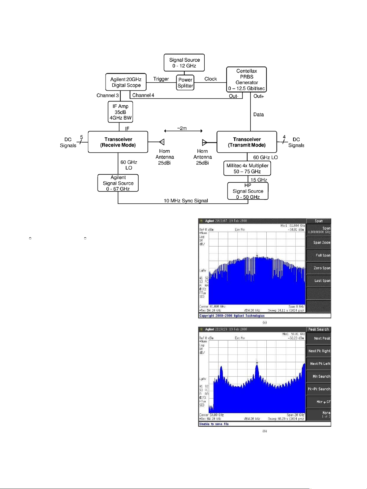
Fig. 19. Diagram of the experimental setup used to demonstrate the wireless link.
system losses have not been de-embedded from the power-
levels measured by the PSA. With the transmitter operating at
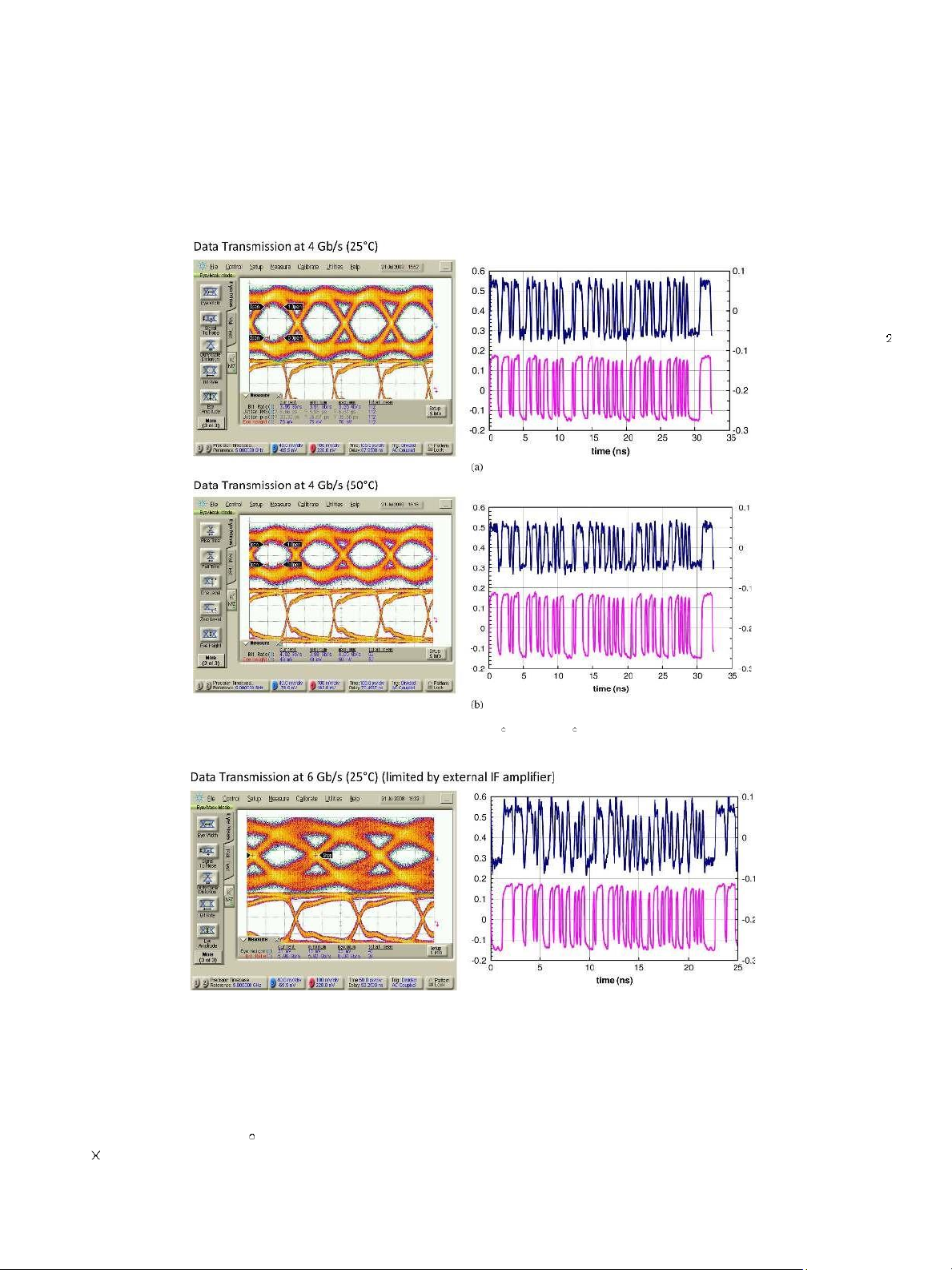
25 C, Fig. 21b(a), and 50 C, Fig. 21b(b), and with an input data-
rate of 4 Gb/s, excellent receive eye diagrams can be seen for
both temperatures, with a clearly recovered bit-pattern. To the
best of our knowledge, this represents the first demonstration of
a 60 GHz transmit/receive link performance over temperature
variation in any silicon technology.
Fig. 20. 4.0 Gb/s PRBS transmitter spectrum at 61 GHz LO (top), and a lower
bit-rate (0.5 Gb/s) modulation spectra at 59 GHz (bottom), showing image
folding due to the use of a harmonic mixer. lOMoAR cPSD| 58977565
TOMKINS et al.: A ZERO-IF 60 GHz 65 nm CMOS TRANSCEIVER WITH DIRECT BPSK MODULATION 2099
Increasing the input data rate to 6 Gb/s, the bandwidth of the
external IF amplifier starts to limit performance, with the eyes
and the received bit-pattern in Fig. 22 indicating the onset of
bandwidth limitations. These transceiver link experiments
demonstrate that the simple, zero-IF, direct-modulation radio
architecture, without ADCs or IQ mixer, is adequate for indoor,
line-of-sight communication at 60 GHz with data rates up to 6
Gb/s over distances that exceed 2 m.
A performance comparison between this work and that of
others is shown in Table I. Due to the general complexities of
the systems and the large variation in implementation levels, an
equitable comparison is difficult to capture in a single table.
While both transceiver and receiver-only half-duplex
performance results for this work are shown for the purpose of
comparing with other receiver-only work, referenced
transceiver publications were not shown in half-duplex mode.
It should be emphasized that, although comparable to other
transceivers, the power consumption of this circuit was not
minimized as a primary design-goal, but rather the operation of
the entire system over process, power-supply, and temperature
variation was pursued. In the authors’ opinion, supported by
recent experimental data collected over temperature by other
groups [37], [38], achieving the required margin for operating
over all corners ultimately results in increased power
consumption. With the exception of [1], most published data
refer to room temperature operation only and may not be
indicative of the expected performance in a real product. lOMoAR cPSD| 58977565
TOMKINS et al.: A ZERO-IF 60 GHz 65 nm CMOS TRANSCEIVER WITH DIRECT BPSK MODULATION 2100 VI. CONCLUSION
for the feasibility of a low-power, low-cost multigigabit/s radio
A 1.2 V 60 GHz zero-IF transceiver with direct modulation that could be integrated in cell-phones and other portable
has been fabricated in a 65 nm CMOS technology. Targeting devices.
high-frequency, high-bandwidth data-transfer applications, the
Fig. 21. The received (top) and transmitted (bottom) eyes and bit sequence for (a) 25 C and (b) 50 C at 61 GHz LO. Minimal degradation is observed between temperature points.
Fig. 22. The received (top) and transmitted (bottom) eyes and bit sequence at 61 GHz LO.
system employs direct digital modulation, a 60 GHz LO ACKNOWLEDGMENT
distribution tree, a fundamental frequency static divider, and
The authors would like to thank K. Laskin and I. Sarkas for
zero-IF down-conversion. A wireless transmit-receive additional measurement assistance and J. Pristupa and CMC for
demonstration over 2 meters between two probe stations acts as CAD support. The authors would also like to acknowledge Dr.
a proof-of-concept, achieving data-transfer rates in excess of 4 W. Walker and Dr. M. Wiklund of Fujitsu Laboratories of
Gb/s when transmitting at 50 C. The transceiver occupies only America Inc. for their support and discussions on digital-rich
1.28 0.81 mm and consumes 101 mW and 131 mW from 1 V mm-wave radio transceivers and the IEEE 802.15.3c standard
supply in receive and transmit mode, respectively, raising hopes specification. lOMoAR cPSD| 58977565
TOMKINS et al.: A ZERO-IF 60 GHz 65 nm CMOS TRANSCEIVER WITH DIRECT BPSK MODULATION 2101 REFERENCES
[21] C. Lee, T. Yao, A. Mangan, K. Yau, M. A. Copeland, and S. P.
Voinigescu, “SiGe BiCMOS 65-GHz BPSK transmitter and 30 to 122
[1] B. Floyd, “Short course: SiGe BiCMOS transceivers for millimeter-
GHz LC-varactor VCOs with up to 21% tuning range,” in Proc. IEEE
wave,” in Proc. Bipolar/BiCMOS Circuits and Technology Meeting
CSICS, Oct. 2004, pp. 179–182. (BCTM), Sep. 2007.
[22] S. Trotta, H. Knapp, D. Dibra, K. Aufinger, T. Meister, J. Bock, W.
[2] D. Alldred, B. Cousins, and S. Voinigescu, “A 1.2 V, 60 GHz radio
Simburger, and A. Scholtz, “A 79 GHz SiGe-bipolar spread-spectrum
receiver with on-chip transformers and inductors in 90 nm CMOS,” in
TX for automotive radar,” in IEEE ISSCC Dig., Feb. 2007, pp. 430–
Proc. IEEE Compound Semiconductor Integrated Circuit Symp. 431.
(CSICS), Nov. 2006, pp. 51–54.
[23] S. Nicolson, A. Tomkins, K. Tang, A. Cathelin, D. Belot, and S.
[3] S. Emami, C. H. Doan, and A. M. Niknejad, “A highly integrated 60
Voinigescu, “A 1.2 V, 140 GHz receiver with on-die antenna in 65 nm
GHz CMOS front-end receiver,” in IEEE Int. Solid-State Circuits
CMOS,” in IEEE Radio Frequency Integrated Circuits (RFIC) Symp. Conf.
Dig. Papers, Jun. 2008, pp. 229–232, Paper RMO3C-2.
(ISSCC) Dig. Tech. Papers, Feb. 2007, pp. 190–191.
[24] K. Tang, S. Leung, N. Tieu, P. Schvan, and S. Voinigescu, “Frequency
[4] C.-H. Wang, H.-Y. Chang, P.-S. Wu, K.-Y. Lin, T.-W. Huang, H. Wang,
scaling and topology comparison of mm-wave CMOS VCOs,” in
and C. H. Chen, “A 60 GHz low-power six-port transceiver for gigabit
Proc. IEEE CSICS, Nov. 2006, pp. 55–58.
software-defined transceiver applications,” in IEEE ISSCC Dig., Feb. 2007, pp. 192–193.
[25] E. Laskin, M. Khanpour, R. Aroca, K. Tang, P. Garcia, and S.
Voinigescu, “95 GHz receiver with fundamental frequency VCO and
[5] S. Pinel, S. Sarkar, P. Sen, B. Perumana, D. Yeh, D. Dawn, and J.
static frequency divider in 65 nm digital CMOS,” in IEEE ISSCC Dig.,
Laskar, “A 90 nm CMOS 60 GHz radio,” in IEEE ISSCC Dig., Feb. Feb. 2008, pp. 180–181. 2008, pp. 130–131.
[26] K. Scheir, G. Vandersteen, Y. Rolain, and P. Wambacq, “A 57-to-66
[6] B. Afshar, Y. Wang, and A. M. Niknejad, “A robust 24 mW 60 GHz
GHz quadrature PLL in 45 nm digital CMOS,” in IEEE ISSCC Dig.,
receiver in 90 nm standard CMOS,” in IEEE ISSCC Dig., Feb. 2008, Feb. 2009. pp. 182–183.
[27] S. Voinigescu, R. Aroca, T. Dickson, S. Nicolson, T. Chalvatzis, P.
[7] A. Parsa and B. Razavi, “A 60 GHz CMOS receiver using a 30 GHz
Chevalier, P. Garcia, C. Garnier, and B. Sautreuil, “Towards a sub-2.5
LO,” in IEEE ISSCC Dig., Feb. 2008, pp. 190–191.
V, 100-Gb/s serial transceiver,” in Proc. IEEE Custom Integrated
[8] M. Tanomura, Y. Hamada, S. Kishimoto, M. Ito, N. Orihashi, K.
Circuits Conf. (CICC), Sep. 2007, pp. 471–478.
Maruhashi, and H. Shimawaki, “TX and RX front-ends for 60 GHz
[28] D. D. Kim, C. Cho, J. Kim, J.-O. Plouchart, and D. Lim, “A low-power
band in 90 nm standard bulk CMOS,” in IEEE ISSCC Dig., Feb. 2008,
mm wave CML prescaler in 65 nm SOI CMOS technology,” in Proc. pp. 558–559. IEEE CSICS, Oct. 2008.
[9] T. Mitomo, R. Fujimoto, N. Ono, R. Tachibana, H. Hoshino, Y.
[29] C. Marcu, D. Chowdhury, C. Thakkar, L. Kong, M. Tabesh, J. Park,
Yoshihara, Y. Tsutsumi, and I. Seto, “A 60-GHzCMOS receiver front-
Y. Wang, B. Afshar, A. Gupta, A. Arbabian, S. Gambini, R. Zamani, A.
end with frequency synthesizer,” IEEE J. Solid-State Circuits, vol. 43,
M. Niknejad, and E. Alon, “A 90 nm CMOS low-power 60 GHz
no. 4, pp. 1030–1037, Apr. 2008.
transceiver with integrated baseband circuitry,” in IEEE ISSCC Dig.,
[10] Y.-W. Chang, H. J. Kuno, and D. L. English, “High data-rate solid- Feb. 2009.
state millimeter-wave transmitter module,” IEEE Trans. Microw.
[30] A. Tomkins, P. Garcia, and S. Voinigescu, “A 94 GHz SPST switch in
Theory Tech., vol. 23, no. 6, pp. 470–477, Jun. 1975.
65 nm bulk CMOS,” in Proc. IEEE CSICS, Oct. 2008, pp. 139–142.
[11] Y.-N. Jen, J.-H. Tsai, T.-W. Huang, and H. Wang, “A V-band
[31] J. W. May and G. M. Rebeiz, “High-performance W-band SiGe RFICs
fullyintegrated CMOS distributed active transformer power amplifier
for passive millimeter-wave imaging,” in IEEE IMS Dig., Jun. 2009.
for IEEE 802.15.TG3c wireless personal area network applications,”
[32] S.-F. Chao, H. Wang, C.-Y. Su, and J. G. J. Chern, “A 50 to 94-GHz
in Proc. IEEE CSICS, Oct. 2008, invited paper.
CMOS SPDT switch using traveling-wave concept,” IEEE Microw.
[12] J. Gilb, “Workshop: Millimeter-wave CMOS radio design for gigabit
Wireless Compon. Lett., vol. 17, no. 2, pp. 130–132, 2007.
wireless applications,” in IEEE IMS, Aug. 2008.
[33] F.-J. Huang and K. O, “A 0.5- m CMOS T/R switch for 900-MHz
[13] P. Eloranta, P. Seppinen, S. Kallioinen, T. Saarela, and A. Parssinen,
wireless applications,” IEEE J. Solid-State Circuits, vol. 36, no. 3, pp.
“A multimode transmitter in 0.13 um CMOS using direct-digital RF 486–492, Mar. 2001.
modulator,” IEEE J. Solid-State Circuits, vol. 42, no. 12, pp. 2774–
[34] H. Takasu, F. Sasaki, H. Kawasaki, H. Tokuda, and S. Kamihashi, “W- 2784, Dec. 2007.
band SPST transistor switches,” IEEE Microw. Guided Wave Lett.,
[14] A. Jerng and C. G. Sodini, “A wideband delta-sigma digital-RF
vol. 6, no. 9, pp. 315–316, 1996.
modulator for high data rate transmitters,” IEEE J. Solid-State
[35] A. Mangan, S. Voinigescu, M. Yang, and M. Tazlauanu, “De-
Circuits, vol. 42, no. 8, pp. 1710–1722, Aug. 2007.
embedding transmission line measurements for accurate modelling of
[15] S. Luschas, R. Schreier, and H.-S. Lee, “Radio frequency digital-to-
1C designs,” IEEE Trans. Electron. Dev., vol. 53, no. 2, pp. 235–241,
analog converter,” IEEE J. Solid-State Circuits, vol. 39, no. 9, pp. 2006. 1462–1467, Sep. 2004.
[36] A. Hazneci and S. Voinigescu, “A 49-Gb/s, 7-tap transversal filter in
[16] S. Sarkar and J. Laskar, “A single-chip 25 pJ/bit multi-gigabit 60 GHz
0.18 m SiGe BiCMOS for backplane equalization,” in Proc. IEEE
receiver module,” in IEEE IMS, Aug. 2007, pp. 475–478.
CSICS, Oct. 2004, pp. 101–104.
[17] T. Dickson, K. Yau, T. Chalvatzis, A. Mangan, R. Beerkens, P.
[37] J.-J. Lin, K.-H. To, B. Brown, D. Hammock, M. Majerus, M. Tutt, and
Westergaard, M. Tazlauanu, M. Yang, and S. P. Voinigescu, “The
W. M. Huang, “Wideband PA and LNA for 60-GHz radio in 90-nm LP
invariance of characteristic current densities in nanoscale MOSFETs
CMOS technology,” in Proc. IEEE CSICS, Oct. 2008.
and its impact on algorithmic design methodologies and design
[38] K. Maruhashi, M. Tanomura, Y. Hamada, M. Ito, N. Orihashi, and S.
porting of Si(Ge) (Bi)CMOS high-speed building blocks,” IEEE J.
Kishimoto, “60-GHz-band CMOS MMIC technology for high-speed
Solid-State Circuits, vol. 41, no. 8, pp. 1830–1845, Aug. 2006.
wireless personal area networks,” in Proc. IEEE CSICS, Oct. 2008,
[18] International Technology Roadmap for Semiconductors, ITRS. invited paper. [Online]. Available:
http://www.itrs.net/Links/2008ITRS/Home2008.htm
[19] T. Yao, M. Gordon, K. Tang, K. Yau, M.-T. Yang, P. Schvan, and S. P.
Voinigescu, “Algorithmic design of CMOS LNAs and PAs for 60-
GHz radio,” IEEE J. Solid-State Circuits, vol. 42, no. 5, pp. 1044– 1057, May 2007.
[20] C. L. Cuccia and E. W. Matthews, “PSK and QPSK modulators for
gigabit data rates,” in MTT-S Int. Microwave Symp. Dig., Jun. 1977,
vol. 77, no. 1, pp. 208–211. lOMoAR cPSD| 58977565
TOMKINS et al.: A ZERO-IF 60 GHz 65 nm CMOS TRANSCEIVER WITH DIRECT BPSK MODULATION 2102
Alexander Tomkins (S’06) received the B.A.Sc.
Yoshiyasu Doi was born in Toyama, Japan, in 1974.
degreeinengineeringphysics fromCarletonUniversity,
He received the B.S. and M.S. degrees from the
Ottawa, Canada, in 2006. He received the M.A.Sc.
Department of Electrical and Electronic Engineering,
degree from the University of Toronto, Toronto, ON,
Tokyo Institute of Technology, Tokyo, Japan, in 1998
Canada, in 2008, where he is currently pursuing the and 2000, respectively.
Ph.D. degree in electrical and electronic engineering.
He joined Fujitsu Laboratories, Ltd., Kanagawa,
In 2008, he worked as a design intern with Fujitsu
Japan, in 2000. He has been engaged in the research
Labs of America on mm-wave wireless transceivers.
and development of CMOS high-speed IO interfaces.
His current research interests include high-frequency
His current interests include mm-wave RF circuits.
passive and active device modeling, passive switch
and attenuator design, and digital-rich mm-wave transceivers.
Sorin P. Voinigescu (M’90–SM’02) received the
Ricardo Andres Aroca received the B.A.Sc. (Hons.)
M.Sc. degree in electronics from the Polytechnic
degree in electrical engineering from the University
Institute of Bucharest, Romania, in 1984, and the
of Windsor, Canada, and the M.A.Sc. degree from the
Ph.D. degree in electrical and computer engineering
University of Toronto, Toronto, ON, Canada, in 2001
from the University of Toronto, Toronto, ON, Canada,
and 2004, respectively. He is currently working in 1994.
toward the Ph.D. degree at the University of Toronto.
From 1984 to 1991, he worked in R&D and
In 2000, he worked as an intern with Nortel
academia in Bucharest, where he designed and
Networks in the Microelectronics Department and
lectured on microwave semiconductor devices and
more recently in 2008 with Alcatel-Lucent in the
integrated circuits. Between 1994 and 2002, he was
High-Speed Electronics Design Research Group,
with Nortel Networks and Quake Technologies in Ottawa, Canada, where he
Bell Laboratories, Murray Hill, NJ. His research
was responsible for projects in high-frequency characterization and statistical
interests lie in the area of 40 to 100 Gb/s transceivers with equalization.
scalable compact model development for Si, SiGe, and III-V devices. He later
Mr. Aroca received the Natural Sciences and Engineering Research Council
conducted research on wireless and optical fiber building blocks and
of Canada (NSERC) Postgraduate Scholarship Award in 2002.
transceivers in these technologies. In 2002, he joined the University of Toronto,
Takuji Yamamoto received the B.S. degree from
where he is a full Professor. His research and teaching interests focus on
Keio-Gijuku University, Tokyo, Japan, in 1986.
nanoscale semiconductor devices and their application in integrated circuits at
In 1986, he joined Fujitsu Laboratories Ltd.
frequencies beyond 200 GHz. During 2008–2009, he spent a sabbatical year at
Japan, where he is currently a Senior Researcher. He Fujitsu Labs of America.
has been engaged in researches on high-speed analog
Dr. Voinigescu received Nortel’s President Award for Innovation in 1996. He
circuits design, especially focusing on the wireline
is a member of the TPCs of the IEEE CSICS and BCTM. He is a co-recipient
communication ICs with operating speed greater than
of the Best Paper Award at the 2001 IEEE CICC and at the 2005 IEEE CSICS,
10 Gb/s, by using several high-speed devices such as
and of the Beatrice Winner Award at the 2008 IEEE ISSCC. His students have
SiGe, GaAs HEMT, and CMOS. He has expanded his expertise into the wireless
won Student Paper Awards at the 2004 VLSI Circuits Symposium, the 2006
area, such as passive UHF radio frequency identification (RFID) tag IC and
SiRF Meeting, RFIC Symposium and BCTM, and at the 2008 International
mm-wave communication IC. His current interests include ultra-high-speed Microwave Symposium.
analog circuit design and mixed-signal ICs using CMOS technology.
Sean T. Nicolson (S’96–M’08) received the B.A.Sc.
degree in electronics engineering from Simon Fraser
University, Canada, in 2001, and the Ph.D. degree in
electrical and computer engineering from the
University of Toronto, Toronto, ON, Canada, in 2008, respectively.
In 2002 he developed low-power integrated circuits
for implantable medical devices at NeuroStream
Technologies. During his Ph.D. work, he held
research internships at the IBM T. J. Watson
Research Center in New York and S.T. Microelec-
tronics in Grenoble, France, where he designed silicon integrated circuits for
applications over 100 GHz. Currently, he is with MediaTek, New York, working
on 60 GHz phased array radio. His research interests include W-band radar,
multi-antenna systems, SiGe HBT devices, and high-speed current mode logic.
Dr. Nicolson has twice been a recipient of scholarships from the National
Science and Engineering Research Council (NSERC), and was the recipient of
the Best Student Paper Award at BCTM 2006.
Tài liệu liên quan:
-

Bài tập quy hoạch mạng hệ thống thu phát vô tuyến môn Thu phát vô tuyến | Học viện Công Nghệ Bưu Chính Viễn Thông
120 60 -
Tài liệu về RF transceiver architectures for W-CDMA systems like UMTS môn Thu phát vô tuyến | Học viện Công Nghệ Bưu Chính Viễn Thông
118 59 -
Tài liệu về Transmit diversity in 3G CDMA systems môn Thu phát vô tuyến | Học viện Công Nghệ Bưu Chính Viễn Thông
119 60 -
Chapter 6 WCDMA môn Thu phát vô tuyến | Học viện Công Nghệ Bưu Chính Viễn Thông
138 69 -
Tài liệu về Introduction to UMTS device testing môn Thu phát vô tuyến | Học viện Công Nghệ Bưu Chính Viễn Thông
120 60